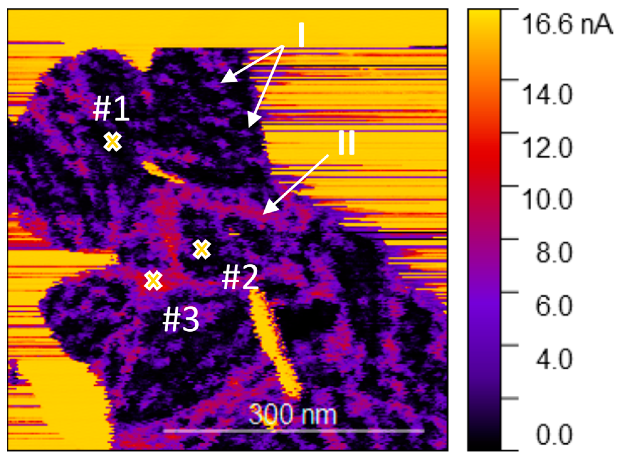
Abstract
Molybdenum trioxide shows many attractive properties, such as a wide electronic band gap and a high relative permittivity. Monolayers of this material are particularly important, as they offer new avenues in optoelectronic devices, e.g., to alter the properties of graphene electrodes. Nanoscale electrical characterization is essential for potential applications of monolayer molybdenum trioxide. We present a conductive atomic force microscopy study of an epitaxially grown 2D molybdenum oxide layer on a graphene-like substrate, such as highly oriented pyrolytic graphite (HOPG). Monolayers were also investigated using X-ray photoelectron spectroscopy, atomic force microscopy (semi-contact and contact mode), Kelvin probe force microscopy, and lateral force microscopy. We demonstrate mobility of the unpinned island under slight mechanical stress as well as shaping and detachment of the material with applied electrical stimulation. Non-stoichiometric MoO3-x monolayers show heterogeneous behavior in terms of electrical conductivity, which can be related to the crystalline domains and defects in the structure. Different regions show various I–V characteristics, which are correlated with their susceptibility to electrodegradation. In this work, we cover the existing gap regarding nanomanipulation and electrical nanocharacterization of the MoO3 monolayer.
1. Introduction
Transition metal oxides, such as molybdenum oxide, are an immensely interesting group of materials due to their unique properties, making them a great candidate for electronic and optical applications [1,2,3]. Orthorhombic MoO3 is an n-type semiconductor with a wide band gap (about 3.2 eV) and a high relative permittivity [4]. Therefore, MoO3 can be used, among others, in batteries, resistive random-access memories, sensors, and organic light-emitting diodes [4,5,6,7,8,9,10,11,12]. An additional important aspect of MoO3 is its layered structure, i.e., its adjacent two-dimensional (2D) crystalline layers are bound by weak van der Waals interactions [2,13]. This allows the easy preparation of ultra-thin films or even monolayers using simple techniques, such as the scotch tape exfoliation method [14], although it has been also successfully grown in 2D form using the hot plate thermal deposition technique [15]. The 2D layers have the potential to be used in flexible and stretchable electronics due to their mechanical properties and transparency [16]. However, a very important issue related to the MoO3 layered structure is the stability of the stretchable or flexible device, especially when the material is under electrical stimulation in complex devices [17].
Investigations of the electrical properties of oxide layers are rare, especially MoO3 on graphene-like substrates, which are predicted to be the optimal electrode material [18,19,20]. Previous studies focused on the description of the mechanical and electrical properties of two or more layers of molybdenum oxide on van der Waals substrates [21,22,23]. Here, we present nanoscale studies of the electrical properties of epitaxial molybdenum oxide monolayer (ML) on highly oriented pyrolytic graphite (HOPG). We investigate the material deposited under ultra-high vacuum conditions, which ensures high purity of the obtained non-stoichiometric and electrically active MoO3 monolayer. We focus on stability and electrical characterization of molybdenum oxide on HOPG, which holds promise in terms of use in nanoelectronic devices. In this work, we use an experimental approach based on nanoscale mechanical and electrical stimulation of 2D material using the atomic force microscopy probes, which allow for both material modification and mapping of its local properties in the same region of the sample. We prove that the application of a local electric potential allows for point-like and precise electrodegradation of the oxide monolayer. As a result of the applied processes, selected areas of the material can be removed without damage to their surroundings. The presented concept of direct modification enables controlled nanolithography of ultrathin oxide layers.
2. Materials and Methods
Molybdenum trioxide was deposited using thermal evaporation on highly oriented pyrolytic graphite (HOPG) (0001), following the procedure described previously [24,25]. HOPG, after being introduced into the ultra-high vacuum system, was exfoliated using the scotch tape method at a pressure of 5 × 10⁻⁸ mbar. The substrate was then annealed at 400 °C for 1 h, and kept at 220 °C during the deposition process. Molybdenum trioxide powder (Sigma-Aldrich, Saint Louis, MO, USA) was evaporated from a Knudsen cell monitored with a thermocouple at 330 °C.
X-ray photoelectron spectroscopy (XPS) was performed using a DAR 400 nonmonochromatic X-ray source (Scienta Omicron, Taunusstein, Germany) with a MgKα (1253.64 eV) anode and a Phoibos 150 (SPECS, Berlin, Germany) hemispherical energy analyzer equipped with a 2D-CCD detector. The pass energy was set to 30 eV, step to 0.1 eV, and dwell to 1.0 s. The resulting spectrum was analyzed using CasaXPS Version 2.3.26rev1.1P (Casa Software Ltd.). The C1s peak (284.5 eV) was used to calibrate the spectra, and the Gaussian–Lorentzian function (80:20) was used for curve fitting.
The samples were investigated with an NT-MDT atomic force microscope (AFM) using the NTEGRA PNL control system (NT-MDT, Moscow, Russia). For semi-contact and Kelvin probe force microscopy (KPFM) mode, golden silicon probes (NSG01, TipsNano, Tallinn, Estonia) were used. For lateral force (LFM), contact, and local conductivity modes, conductive Pt/Ir coated probes (PPP-CONTPt, Nanosensors, Neuchatel, Switzerland) were used. In semi-contact mode, we were focusing on topography and contact potential difference. In contact mode, the scanning speed was set to about 12 μm/s and as low as possible setpoint. Additionally, images of lateral forces are well resolved at the given parameters. Current measurements were carried out with a grounded probe, and bias voltage was applied to the HOPG substrate. The acquisition time for I–V curves (forward and backward) was set to 1 s. Current values above 10 nA are logarithmic to represent conduction dynamics at both low and high currents. All examinations were performed under ambient or low vacuum (~0.3 mbar) conditions. The AFM images were processed in Gwyddion 2.59 software (Brno, Czech Republic) [26].
3. Results
3.1. Chemical Analysis of MoO3-x Monolayer
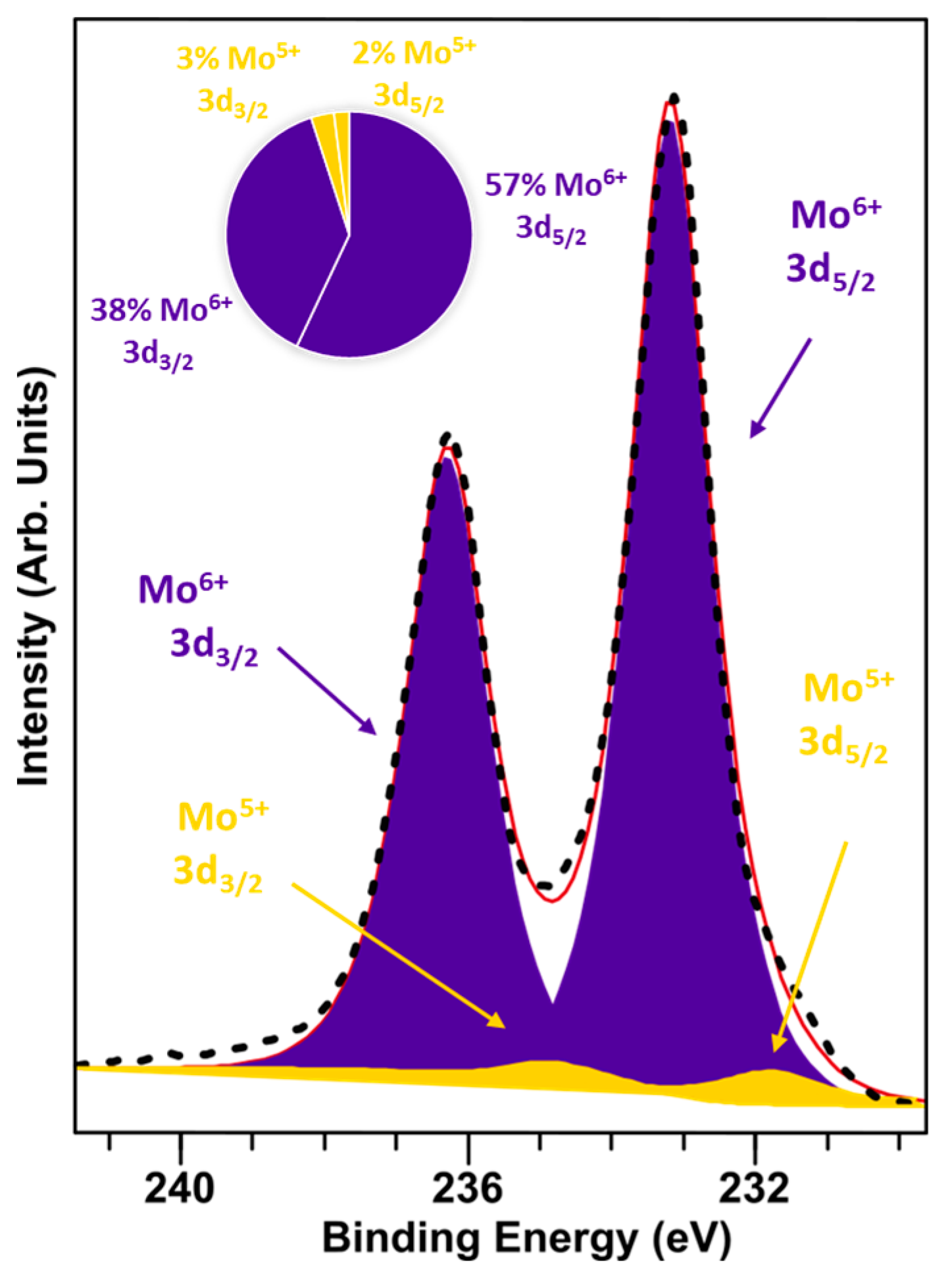
XPS spectra was acquired on the MoOx-3 monolayer on the HOPG sample, which was transferred between the UHV deposition system and the analytical UHV system using a vacuum suitcase (pressure at the level 5 × 10⁻⁸ mbar) to avoid air exposure. Figure 1 shows the Mo 3d XPS spectrum, which consists of two components, where about 95% is represented by Mo6+ from the 3d5/2 component at the 233.2 eV binding energy position and 5% is Mo5+ 3d5/2 at 231.8 eV. The Mo4+ component is not present. Although the material is non-stoichiometric, it has not been reduced to MoO2. This non-stoichiometric growth may be caused by the deposition conditions, i.e., both substrate and deposition temperatures can lead to an oxygen deficiency in the molybdenum oxide layer in UHV [18]. The oxygen vacancies could preferentially be created in grain boundaries of oxide or at the location of substrate structural defects [27]. The observed non-stoichiometry is known to lead to the formation of additional states in the band gap and in consequence increase the material electrical conductivity [24]. Greiner et al. [28] investigated changes in work function and band structure of MoO3. The electronic structure of this material is sensitive to the oxidation state of the molybdenum cation. Stoichiometric MoO3 has a wide band gap of about 3.2 eV and the Mo 4d band is considered empty. A non-stoichiometric material with a non-zero vacancy density means that in addition to Mo6+ cations, Mo5+ cations are also present in the structure. The presence of Mo5+ cations leads to a partially occupied Mo 4d band.

Figure 1.
XPS Mo 3d spectrum fitted with two components (Mo5+ and Mo6+ in a 5:95 ratio).
3.2. Morphology and Stability of MoO3-x Monolayers
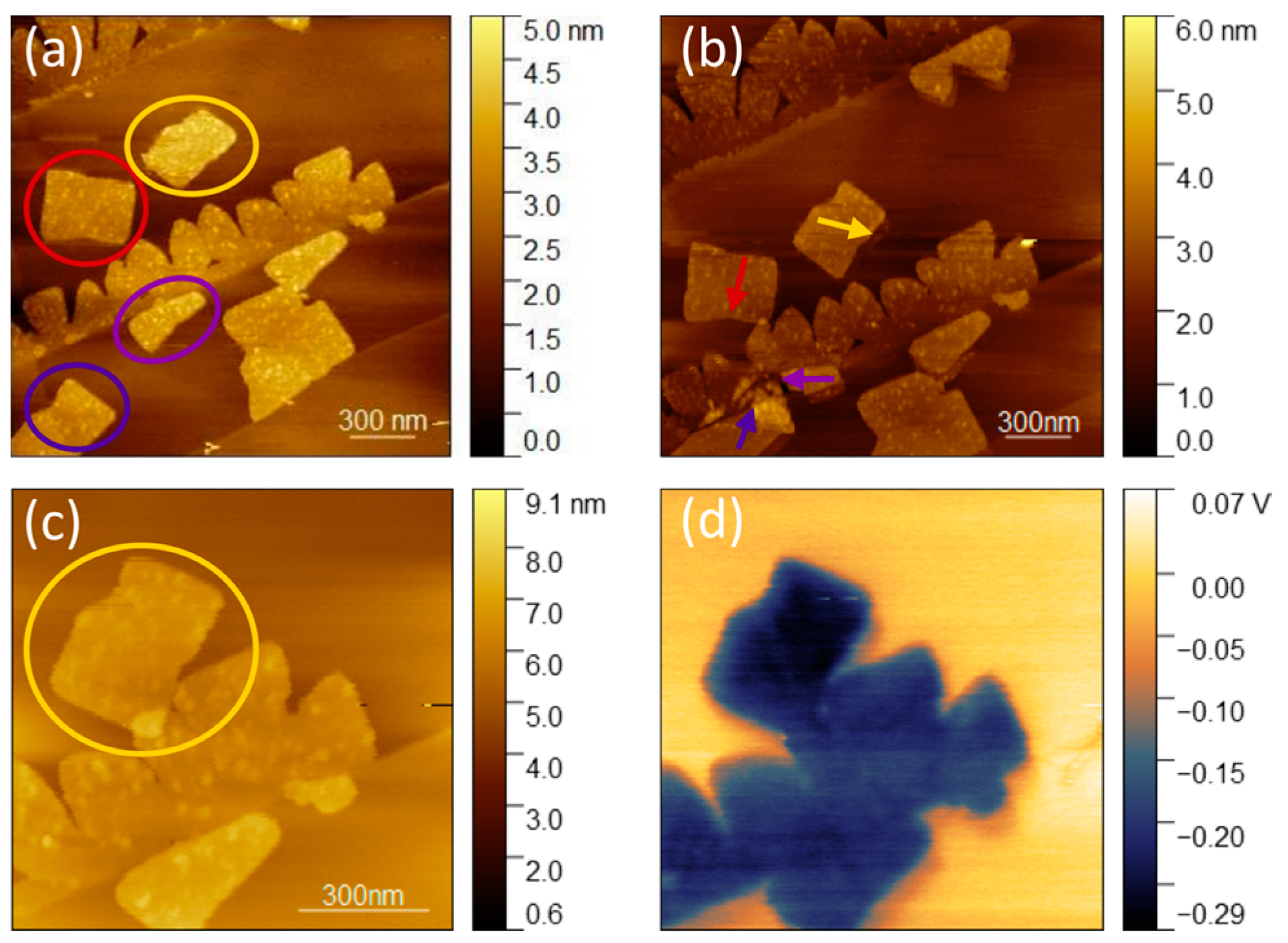
The deposition conditions used to achieve single monolayers of MoO3-x on HOPG have been described already in our previous work [24,25] where it was shown that the growth parameters were optimized to reach a high degree of crystallinity in MoO3-x. Note that by monolayer of MoO3-x, we refer to a structure corresponding to half the height of the unit cell of bulk α-MoO3. The crystalline nature of the monolayers was demonstrated using STM (see Figure 1 in [24]) and high-resolution transmission electron microscopy (see Figure S1 in [25]), successfully identifying the presence of α-MoO3. Statistical analysis on the thickness of the MoO3-x layer based on atomic force microscopy and scanning tunnelling microscopy (STM) images performed under UHV conditions confirms that the thickness of the islands is approximately 0.7 nm (see height histogram in Figure S1 of [24]). However, after exposure to air, local perturbations are visible on the surface of the layer, which appear as higher (brighter) spots on the flakes presented in Figure 2, and may be associated with structural defects as previously described in the case of the attachment of hydrogen [29].

Figure 2.
Semi-contact AFM and Kelvin probe force microscopy images of MoO3-x on HOPG: (a) topography with mobile MoO3-x islands marked using ovals; (b,c) topography with next locations of islands; (d) contact potential difference corresponding to (c). Arrows on (b) represent the sliding direction of each island. Image (c) shows the final location of the island marked with a yellow oval on image (a).
The oxide flakes grow preferentially at the edges of the HOPG steps, often forming clusters of multiple, interconnected islands. There are also unpinned islands that grow away from the HOPG steps (see islands indicated using yellow and red ovals in Figure 2a).
All the images in Figure 2 were acquired with the same scanning direction, where left-to-right and bottom-to-top are the fast and slow scanning directions, respectively. Despite the relatively small probe–sample interactions in the semi-contact imaging mode, lateral movement of MoO3-x islands on the substrate was visible in our experiments. In Figure 2a, four islands are marked with yellow, red, purple, and blue ovals. In the next images (Figure 2b,c), it is shown how these islands are moved scan after scan. The motion of the AFM probe is the same in all scans; however, each island appears to undergo a sliding motion along independent sliding directions and angles of rotation (arrows marked on Figure 2b show the sliding directions). As the scanning progresses, the moved islands approach the islands located at the step edges, and in some cases even overlap with them. The islands marked with purple and blue ovals also overlap the islands located along the HOPG step. However, in this case, islands interact and the island located along the step starts to deform. Moreover, the purple one is degraded when moved. Such AFM manipulations can be explained by the weak van der Waals interactions between the substrate and the molybdenum oxide islands, which means that the energy barriers for sliding are sufficiently low to be overcome by the probe–sample interactions. If both materials are defect-free, there are no chemical bonds between the substrate and oxide layer, and in consequence the islands are stabilized only via the van der Waals interactions. Additionally, since HOPG has a small friction coefficient [30], it is expected that the AFM probe can push or pull some of the islands. Note, however, that such relocations were relatively rare in our experiments. The majority of the islands are pinned to HOPG step edges and thus are not prone to relocation. The observed dynamic behavior is consistent with the high chemical stability of the synthesized material under mechanical stress, as they retain their shape despite undergoing motion.
Surface potential analysis of molybdenum oxide on HOPG (Figure 2d) performed in air indicates contact potential difference (CPD) between the substrate and the layer of about 0.25 V. CPD for MoO3-x on HOPG measured in UHV is at the level of 1.8 V [25], which is considerably larger. This indicates that the air exposure leads to a reduction in the effective work function, which agrees with previous experimental results [31]. In Figure 2d, the yellow color corresponds to the higher CPD value on HOPG and the blue color corresponds to the lower CPD value on the MoO3-x monolayer. Slight CPD inhomogeneities in molybdenum oxide are also visible, which may be the result of oxygen vacancies and hydrogenation [29,32]. The in-plane resolution of the CPD measurement in air is not sufficient; nonetheless, some perturbations visible on topography can be assigned to slightly higher CPD values than in other regions of the island.
As mentioned earlier, in semi-contact mode, the islands are sliding on the HOPG surface by the forces exerted by the probe. The electrical properties of molybdenum oxide monolayers were investigated in local conductivity contact mode of atomic force microscopy. In contact mode, the interaction is higher, and in some case the AFM probe can even lead to removal of the islands from the scan area (not shown here). Therefore, appropriate scanning parameters must be carefully selected to characterize MoO3-x monolayers on HOPG in this mode.
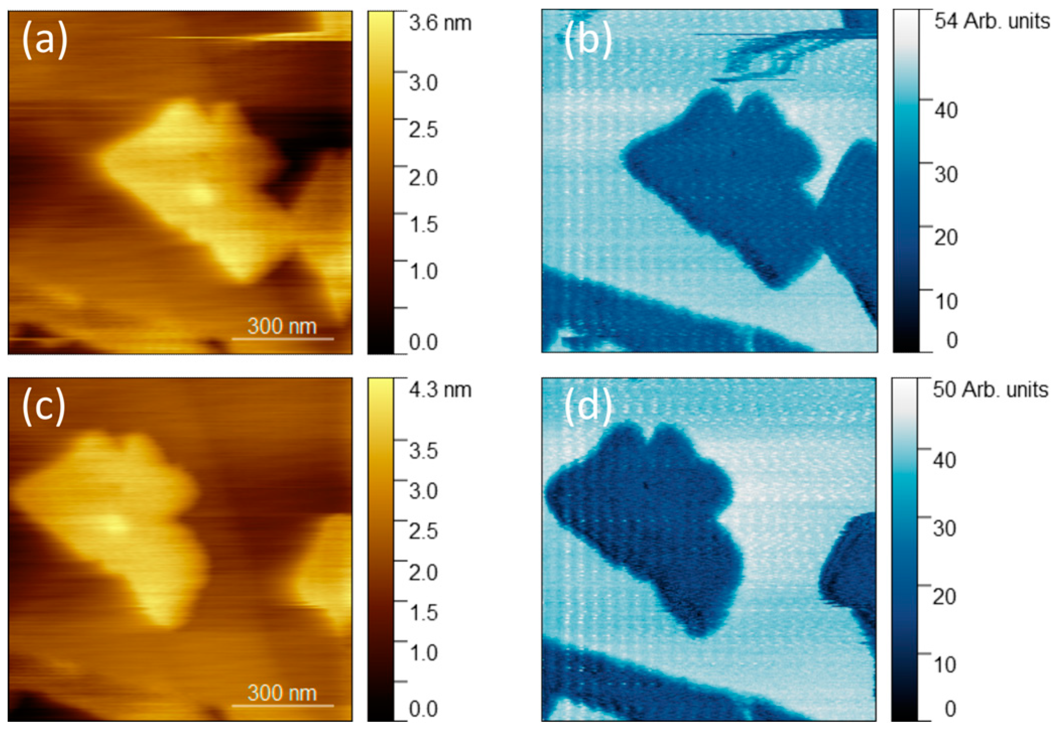
Images of topography and lateral force shown in Figure 3a–d, respectively, were obtained with a scanning speed set at 12 μm/s and a negative setpoint, i.e., in adhesion force regime. High scanning rate and low setpoint hinder resolution of the topographic images significantly. However, in the lateral-force images, we can observe well-resolved contrast (Figure 3b,d). In Figure 3a,c, the islands appear homogeneous—there are no visible perturbations as in the case of semi-contact (see Figure 2). This may be due to the considerably lower quality of the topography images obtained in contact AFM mode. With an applied voltage of 1 V and 0.6 V (Figure 3a–d, respectively), the island was highly mobile but did not degrade, which was consistent with the observations in semi-contact imaging mode. Higher scanning voltages exceeding 1 V led to complete layer removal (not shown here). Additionally, it is worth noting traces of a sliding island in the upper right corner in Figure 3a,b. Similar observations were discussed by Kim et al. in [21], where whole monolayer-thick films were removed or partially destroyed during scanning, in contrast to our results here where we show that they are sliding over the HOPG surface. The island has significantly changed its position during one scan. At the time of the scans, the movement of the island usually occurred during the course of a single measuring line, which made their movement best described by discontinuous “hops” rather than by gradual sliding. Other two-dimensional materials have been reported to display such sudden and abrupt displacement patterns [33]. Note that we observed that the MoO3-x islands that grew along the HOPG steps are less mobile. Such islands have the benefit of mechanical adherence and were thus chosen for further analyses, during which we performed local electrical stimulation of the MoO3-x monolayers with the AFM probe.

Figure 3.
Topography (a,c) and lateral force (b,d) image of MoO3-x on HOPG, performed in contact mode AFM: (a,b) first image with original position of MoO3-x island; (c,d) new position of the island after movement. The scanning voltages are 1 V (a,b) and 0.6 V (c,d).
3.3. Electrical Characterisation
To investigate electrical properties, current–voltage curves were acquired for point measurements on molybdenum oxide. The bottom electrode was HOPG, which was biased, and the top electrode was a conductive Pt/Ir-coated AFM probe (grounded), which enables point measurements and surface characterization before and after current stimulation. Figure 4 shows AFM images of topography and lateral force taken at 0.5 V. Point I–V measurements were taken at part marked with white square of the original island, while the effect of that electrostimulation is depicted in Figure 4c,d. It can be observed that electrical stimulation leads to the removal of a small region of material, or a separation of a part of the island (Figure 4c,d). Electrical stimulation of the interior of the islands leads to the formation of topographic holes (Figure 4c, #1–#4, #6), the size of which depends on the voltage range of the stimulation, which will be discussed later. The lateral force image further confirms the local removal of MoO3-x. Figure 4d shows that the lateral force at points #1 and #6 are in agreement with those observed for HOPG. We now focus on a more complex process that combines electrical and mechanical stimulation. Point #3, where a hole has also been created, is also the starting point of tearing off the part of the island. This displacement, caused by mechanical and electrical interaction with the tip, allows for intentional nanomanipulation and geometry modification.
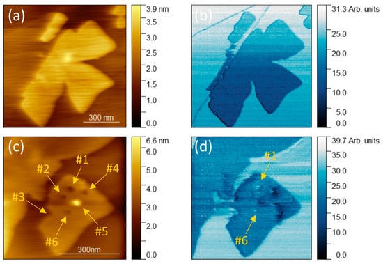
Figure 4.
Topography and lateral force microscopy images: (a) topography and (b) lateral force image of MoO3-x monolayer before point I–V measurement; (c) topography and (d) lateral force image of MoO3-x monolayer after point I–V measurement. Images were acquired with 0.5 V bias applied to the sample. The white square in image (b) shows the area shown in image (c,d).
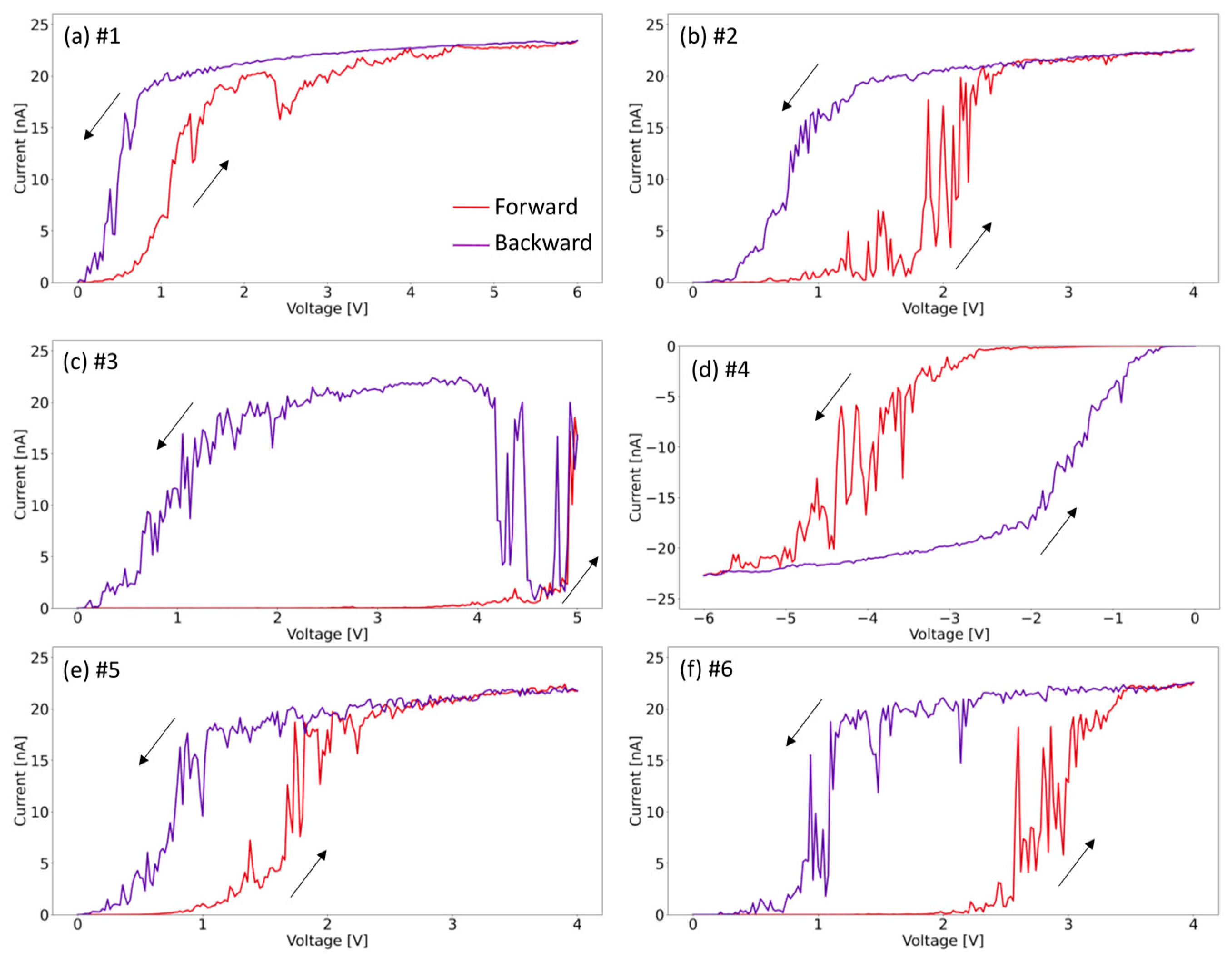
Figure 5 shows the current–voltage (I–V) curves, which were acquired at six different points with various voltage ranges applied. The curves correspond to the locations marked in Figure 4c, where the (a) curve corresponds to point #1, (b) curve to point #2, etc. Note that the forward red curve is acquired from 0 V to the applied voltage, and the backward purple curve from the applied voltage to 0 V. The arrows in Figure 5 indicate the acquisition direction of the I–V curve. In Figure 5a, it can be seen that molybdenum oxide initial conductivity (red forward I–V curve) is relatively high at a low voltage of about 0.3 V compared to other curves, which suggests nonhomogeneous electrical properties of the material. For all points, however, sweeping to 4–6 V leads to modification of the layer, which is visible as a significant decrease in the resistivity observed in I–V curves (see purple backward curve). This occurs regardless of the direction of the applied polarization and in most cases is related to removal of a small region of the layer. Initially, the material is non-stoichiometric, with a certain defect density in the structure, leading to the formation of states in the band gap [28]. We believe that applying a sufficiently large voltage introduces more defects into the stimulated region, leading to a further increase in conductivity. Past a certain potential threshold, the local material removal is attributed to electrodegradation and decomposition of the layer. In Figure 5, only the first sweeps are shown, since subsequent curves measured at the same locations are characterized with a permanent high conductivity, without hysteresis behavior (see Figure S1 in Supplementary Materials). These permanently modified I–V curves are characteristic of HOPG, which is an additional argument indicating the local removal of the material; confirming the observations from the topography and lateral force images. Only in the case of curve #5, the next curve indicates a decrease in conductivity, which indicates the shedding of removed earlier material seen at point #5 in Figure 4c. Furthermore, the magnitude of the voltages used for the I–V curves seems to influence the size of the removed area. The holes at points #1 and #4, where +6 V and −6 V polarizations were used, are wider than #2 and #6, for which the polarization was only +4 V. This suggest that the material removing mechanism is related to electrodegradation of molybdenum oxide supported by dissipation of Joule heat in a relatively small volume characteristic of 2D materials. By changing the value of the applied voltage, it is possible to control the amount of material to be removed. Therefore, controllable local current stimulation can be used as a tool to precisely remove parts of the MoO3-x monolayer with a nanoscale precision.

Figure 5.
I–V curves acquired at the points shown in Figure 4c at applied voltage of: (a) 6 V; (b) 4 V; (c) 5 V; (d) −6 V; (e) 4 V; (f) 4V. Forward curves are shown in red and backward curves in purple. All curves start or finish at 0 V.
The current–voltage curves shown in Figure 5 show a variety of characteristics. The material is non-stoichiometric, therefore there are areas with larger output conductivity and areas with relatively lower output conductivity, depending on the local concentration of defects. Table 1 summarizes the activation voltage to a current of 10 nA. For curves #1, #2, and #5, the activation voltages are relatively low: 1.1 V, 2.1 V, and 1.8 V, respectively. This may indicate that the material initially possessed higher defect densities in these areas, causing a higher conductivity and a lower activation voltage. For curves #3, #4, and #6, the activation voltage is above 3 V, and the material remains non-conductive across a larger voltage range, especially in the case of curve #3. For this particular location, the activation voltage is the highest and is 4.9 V.

Table 1.
Activation voltage to 10 nA current corresponding to forward (red) curves shown on Figure 5.
Next, to obtain a high-resolution conductivity map of the material, the sample was examined under low vacuum conditions (0.3 mbar) to remove the adsorbed ambient water, which otherwise affects the electrical characterization and increases probe contamination. The conductivity map presented in Figure 6 highlights the high heterogeneity of the conductivity of the MoO3-x monolayer on HOPG. The areas in black are nearly non-conductive (for a polarization of 0.2 V), with spots (marked as I) and lines (marked as II) of higher conductivity, indicated in purple and red. These non-homogeneities are arranged similarly to the local perturbations seen in the semi-contact topography (see Figure 2c for example); and therefore, the higher conductivity at these locations may be due to the changes in chemical composition, similarly to a previous report on hydrogen accumulation [25]. However, the elongated domains with higher conductivity may correspond to grain boundaries resulting from independent MoO3-x islands merging during the growth, which are preferably decorated by vacancies or MoO3 suboxides. The observed conductivity is in agreement with XPS analysis, indicative of the slightly non-stoichiometric nature of the synthesized material.
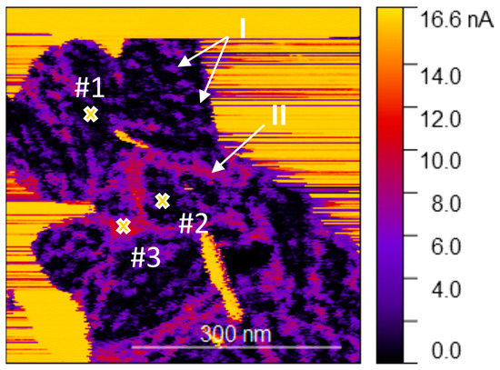
Figure 6.
Conductivity map of the MoO3-x monolayer on HOPG with the location of the three I–V measurement points indicated. The image was acquired with a bias of 0.2 V on the sample.
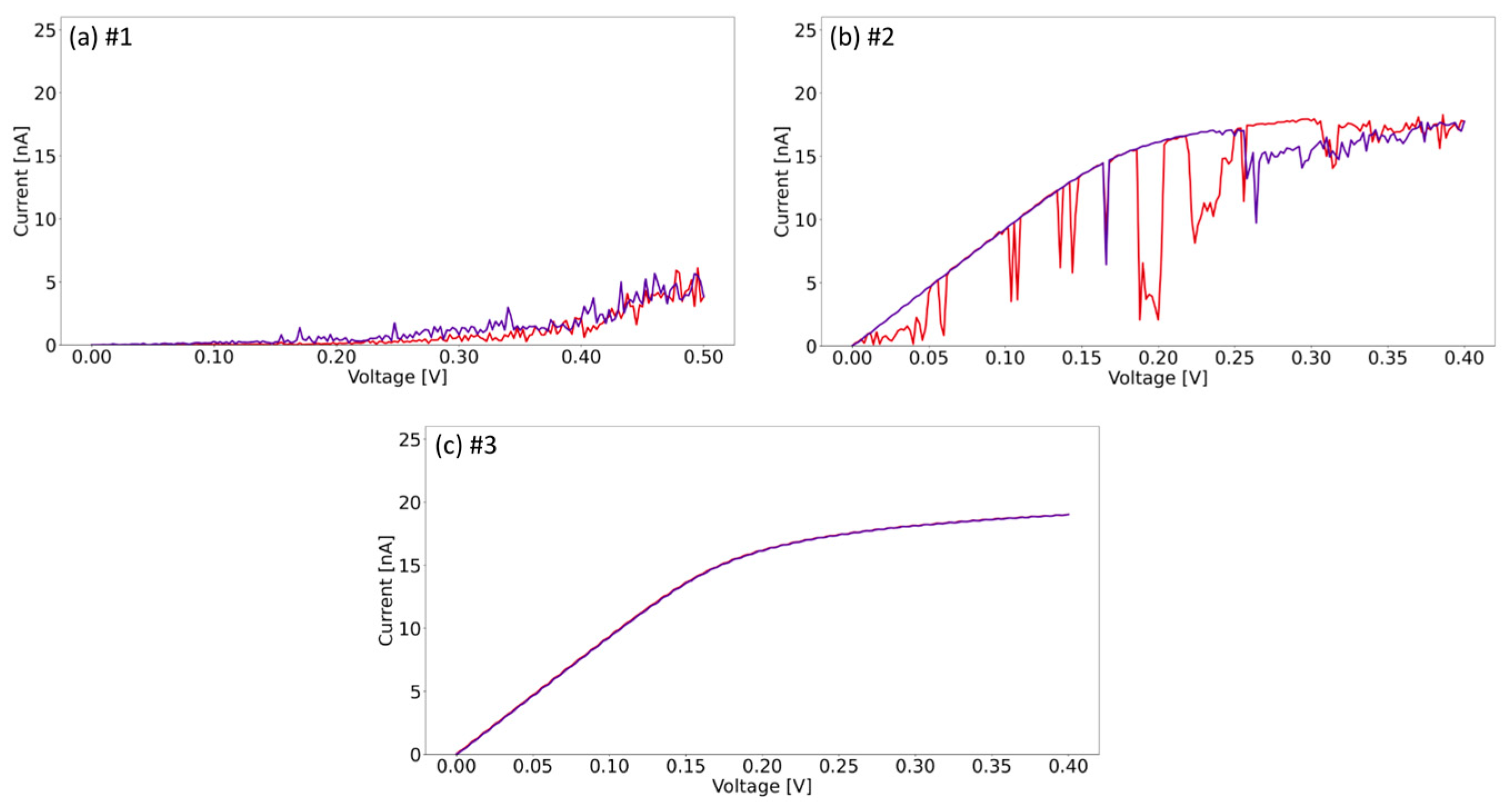
To shed more light on the electrical properties of the individual areas observed on the conductivity map, we further analyze the I–V curves in three selected areas. Additionally, to enable characterization and to avoid material removal, which also leads to permanent tip degradation, the I–V curves were performed up to a voltage of 0.5 V only. By this, we investigate three representative areas we found on MoO3-x monolayers from non-conductive to conductive. Figure 7 shows the I–V curves recorded for the regions indicated #1–3 in Figure 6. The curve shown in Figure 7a, which corresponds to point #1 located in a low conductivity region, is close to 0 nA within the applied voltage range. The I–V curve is consistent with the conductivity map and indicates a low conductivity in comparison to the other locations. Curve (b) corresponds to point #2, where the conductance is much higher in the corresponding voltage values; however, the tip–sample junction is relatively unstable, as shown by the presence of abrupt changes in the conductance. Point #2 is located in the area of non-conductive material tightly surrounded with slightly conductive spots, which are likely to impact the electrical behavior. The measurement over the reddish line at point #3 (Figure 7c) shows a nearly ohmic behavior with the current nearly saturating. Note that the current converter used for the presented measurements is logarithmic above 10 nA, which determines the shape of the curve. Our findings based on these three examples confirm previous observations that the material is electrically heterogeneous and may have different local susceptibilities to electrical stimulation. This was shown with different behavior during electrically stimulated removing of material, but regardless of this heterogeneity, the material at all points exhibits sufficient susceptibility to be nanolithographed effectively, as long as the threshold voltage is set at a level adapted to the least conductive areas.
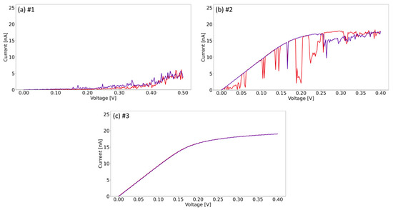
Figure 7.
I–V curves corresponding to the measurement of the points shown in Figure 6: (a) 0.5 V; (b) 0.4 V; (c) 0.4 V. Forward curves are shown in red and backward curves in purple. All curves start or finish at 0 V.
4. Conclusions
We showed that a 2D layer of molybdenum oxide on a graphite substrate can be easily modified at the nanoscale using the AFM probe. While a slight mechanical stress in semi-contact mode causes the unpinned islands to slide across the surface of the substrate, some of the small islands located along the HOPG step also were also successfully moved. The addition of electrical stimulation in contact mode allows the material to be detached and shaped. We attribute this effect to electrodegradation of the oxide material. Additionally, adding a polarization during the sliding of island on the substrate leads to a more abrupt behavior. At the same time, we showed that slightly non-stoichiometric monolayers of MoO3 are heterogeneous in terms of electrical conductivity at the nanoscale. XPS analysis of MoO3 on HOPG showed a noticeable concentration of molybdenum in the 5+ oxidation state, which is associated to the oxygen vacancies in the crystalline structure, locally increasing the conductivity.
Our research demonstrated the possibilities of modifying and shaping ultra-thin nanoscale oxide layers, with a focus on defects. Our findings contribute to important aspects of utilizing binary MoO3 in applications such as graphene-based electrodes, stressing that potential devices should be designed taking into account the nanoscale heterogeneity of the material.
Supplementary Materials
The following are available online at https://www.mdpi.com/article/10.3390/cryst13060905/s1, Figure S1: Subsequent I–V curves (acquired immediately after the curves shown in Figure 4c) corresponding to the measurement of the same points with an applied voltage of: (a) 6 V; (b) 4 V; (c) 5 V; (d) −6 V; (e) 4 V; (f) 4V.
Author Contributions
Conceptualization A.N. and M.R., Sample preparation, XPS measurement, AFM scans, writing—original draft preparation A.N., methodology of oxides growth D.A.K., data analyses and selection A.N, M.R. and D.A.K., result discussion and manuscript review and editing A.N., M.R., D.A.K., P.J.K., M.L.S., I.L., M.P., P.K., P.D., W.K., R.D., P.P., W.R. and K.T., supervision M.R. and P.J.K., founding acquisition M.R. All authors have read and agreed to the published version of the manuscript.
Funding
This work was supported by National Science Center, Poland, under the Grant 2020/38/E/ST3/00293.
Data Availability Statement
Not applicable.
Acknowledgments
Not applicable.
Conflicts of Interest
The authors declare no conflict of interest.
References
- Alam, H.; Chowdhury, S.; Roy, A.; Wu, X.; Ge, R.; Rodder, M.A.; Chen, J.; Lu, Y.; Stern, C.; Houben, L.; et al. Wafer-Scalable Single-Layer Amorphous Molybdenum Trioxide. ACS Nano 2022, 16, 3756–3767. [Google Scholar] [CrossRef] [PubMed]
- Hu, X.; Liu, K.; Cai, Y.; Zang, S.-Q.; Zhai, T. 2D Oxides for Electronics and Optoelectronics. Small Sci. 2022, 2, 220008. [Google Scholar] [CrossRef]
- Zhou, F.; Zhou, Z.; Chen, J.; Choy, T.H.; Wang, J.; Zhang, N.; Lin, Z.; Yu, S.; Kang, J.; Wong, H.S.P.; et al. Optoelectronic Resistive Random Access Memory for Neuromorphic Vision Sensors. Nat. Nanotechnol. 2019, 14, 776–782. [Google Scholar] [CrossRef]
- Balendhran, S.; Deng, J.; Ou, J.Z.; Walia, S.; Scott, J.; Tang, J.; Wang, K.L.; Field, M.R.; Russo, S.; Zhuiykov, S.; et al. Enhanced Charge Carrier Mobility in Two-Dimensional High Dielectric Molybdenum Oxide. Adv. Mater. 2013, 25, 109–114. [Google Scholar] [CrossRef] [PubMed]
- Kröger, M.; Hamwi, S.; Meyer, J.; Riedl, T.; Kowalsky, W.; Kahn, A. Role of the Deep-Lying Electronic States of MoO3 in the Enhancement of Hole-Injection in Organic Thin Films. Appl. Phys. Lett. 2009, 95, 123301. [Google Scholar] [CrossRef]
- Rahman, F.; Zavabeti, A.; Rahman, M.A.; Arash, A.; Mazumder, A.; Walia, S.; Sriram, S.; Bhaskaran, M.; Balendhran, S. Dual Selective Gas Sensing Characteristics of 2D α-MoO3-x via a Facile Transfer Process. ACS Appl. Mater. Interfaces 2019, 11, 40189–40195. [Google Scholar] [CrossRef]
- Ma, Z.; Shi, X.M.; Nishimura, S.; Ko, S.; Okubo, M.; Yamada, A. Anhydrous Fast Proton Transport Boosted by the Hydrogen Bond Network in a Dense Oxide-Ion Array of α-MoO3. Adv. Mater. 2022, 34, 2203335. [Google Scholar] [CrossRef] [PubMed]
- Huang, F.; Liu, H.; Li, X.; Wang, S. Enhancing Hole Injection by Processing ITO through MoO3 and Self-Assembled Monolayer Hybrid Modification for Solution-Processed Hole Transport Layer-Free OLEDs. Chem. Eng. J. 2022, 427, 131356. [Google Scholar] [CrossRef]
- Marchal, W.; Verboven, I.; Kesters, J.; Moeremans, B.; De Dobbelaere, C.; Bonneux, G.; Elen, K.; Conings, B.; Maes, W.; Boyen, H.G.; et al. Steering the Properties of MoOx Hole Transporting Layers in OPVs and OLEDs: Interface Morphology vs. Electronic Structure. Materials 2017, 10, 123. [Google Scholar] [CrossRef]
- Hosseini, M.A.; Ranjbar, M. Optical Hydrogen Sensing by MoO3 Films Deposited by a Facile Flame Synthesis Method. Appl. Surf. Sci. 2023, 618, 156641. [Google Scholar] [CrossRef]
- Cheng, P.; Shi, L.; Li, W.; Fang, X.; Cao, D.; Zhao, Y.; Cao, P.; Liu, D.; He, D. Efficient Regulation of Polysulfides by MoS2/MoO3 Heterostructures for High-Performance Li-S Batteries. Small 2023, 19, 2206083. [Google Scholar] [CrossRef] [PubMed]
- Yun, Q.; Ge, Y.; Chen, B.; Li, L.; Wa, Q.; Long, H.; Zhang, H. Hybridization of 2D Nanomaterials with 3D Graphene Architectures for Electrochemical Energy Storage and Conversion. Adv. Funct. Mater. 2022, 32, 2202319. [Google Scholar] [CrossRef]
- de Castro, I.A.; Datta, R.S.; Ou, J.Z.; Castellanos-Gomez, A.; Sriram, S.; Daeneke, T.; Kalantar-zadeh, K. Molybdenum Oxides—From Fundamentals to Functionality. Adv. Mater. 2017, 29, 1701619. [Google Scholar] [CrossRef]
- Holler, B.A.; Crowley, K.; Berger, M.H.; Gao, X.P.A. 2D Semiconductor Transistors with Van Der Waals Oxide MoO3 as Integrated High-κ Gate Dielectric. Adv. Electron. Mater. 2020, 6, 2000635. [Google Scholar] [CrossRef]
- Molina-Mendoza, A.J.; Lado, J.L.; Island, J.O.; Niño, M.A.; Aballe, L.; Foerster, M.; Bruno, F.Y.; López-Moreno, A.; Vaquero-Garzon, L.; Van Der Zant, H.S.J.; et al. Centimeter-Scale Synthesis of Ultrathin Layered MoO3 by van Der Waals Epitaxy. Chem. Mater. 2016, 28, 4042–4051. [Google Scholar] [CrossRef]
- Cho, E.; Cha, S.; Kim, Y.; Kim, C. Transparent and Flexible Electrode Composed of a Graphene Multilayer Interlayer-Doped with MoO3. Org. Electron. 2020, 77, 105437. [Google Scholar] [CrossRef]
- Choi, D.K.; Kim, D.H.; Lee, C.M.; Hafeez, H.; Sarker, S.; Yang, J.S.; Chae, H.J.; Jeong, G.W.; Choi, D.H.; Kim, T.W.; et al. Highly Efficient, Heat Dissipating, Stretchable Organic Light-Emitting Diodes Based on a MoO3/Au/MoO3 Electrode with Encapsulation. Nat. Commun. 2021, 12, 2864. [Google Scholar] [CrossRef]
- Wu, Q.H.; Zhao, Y.; Hong, G.; Ren, J.G.; Wang, C.; Zhang, W.; Lee, S.T. Electronic Structure of MoO3-x/Graphene Interface. Carbon 2013, 65, 46–52. [Google Scholar] [CrossRef]
- Krukowski, P.; Piskorski, M.; Udovytska, R.; Kowalczyk, D.A.; Lutsyk, I.; Rogala, M.; Dąbrowski, P.; Kozłowski, W.; Łuszczyńska, B.; Jung, J.; et al. Graphene on Quartz Modified with Rhenium Oxide as a Semitransparent Electrode for Organic Electronics. Opto-Electron. Rev. 2022, 30, e141953. [Google Scholar] [CrossRef]
- Krukowski, P.; Kowalczyk, D.A.; Piskorski, M.; Dabrowski, P.; Rogala, M.; Caban, P.; Ciepielewski, P.; Jung, J.; Baranowski, J.M.; Ulanski, J.; et al. Work Function Tunability of Graphene with Thermally Evaporated Rhenium Heptoxide for Transparent Electrode Applications. Adv. Eng. Mater. 2020, 22, 1900955. [Google Scholar] [CrossRef]
- Kim, J.H.; Hyun, C.; Kim, H.; Dash, J.K.; Ihm, K.; Lee, G.H. Thickness-Insensitive Properties of α-MoO3 Nanosheets by Weak Interlayer Coupling. Nano Lett. 2019, 19, 8868–8876. [Google Scholar] [CrossRef] [PubMed]
- Kim, J.H.; Dash, J.K.; Kwon, J.; Hyun, C.; Kim, H.; Ji, E.; Lee, G.H. Van Der Waals Epitaxial Growth of Single Crystal α-MoO3 Layers on Layered Materials Growth Templates. 2D Mater. 2019, 6, 015016. [Google Scholar] [CrossRef]
- Cai, L.; McClellan, C.J.; Koh, A.L.; Li, H.; Yalon, E.; Pop, E.; Zheng, X. Rapid Flame Synthesis of Atomically Thin MoO3 down to Monolayer Thickness for Effective Hole Doping of WSe2. Nano Lett. 2017, 17, 3854–3861. [Google Scholar] [CrossRef] [PubMed]
- Kowalczyk, D.A.; Rogala, M.; Szałowski, K.; Kozłowski, W.; Lutsyk, I.; Piskorski, M.; Krukowski, P.; Dabrowski, P.; Belić, D.; Cichomski, M.; et al. Local Electronic Structure of Stable Monolayers of α-MoO3−x Grown on Graphite Substrate. 2D Mater. 2021, 8, 025005. [Google Scholar] [CrossRef]
- Kowalczyk, D.A.; Rogala, M.; Szałowski, K.; Belić, D.; Dąbrowski, P.; Krukowski, P.; Lutsyk, I.; Piskorski, M.; Nadolska, A.; Krempiński, P.; et al. Two-Dimensional Crystals as a Buffer Layer for High Work Function Applications: The Case of Monolayer MoO3. ACS Appl. Mater. Interfaces 2022, 14, 44506–44515. [Google Scholar] [CrossRef]
- Nečas, D.; Klapetek, P. Gwyddion: An Open-Source Software for SPM Data Analysis. Cent. Eur. J. Phys. 2012, 10, 181–188. [Google Scholar] [CrossRef]
- McKenna, K.; Shluger, A. The Interaction of Oxygen Vacancies with Grain Boundaries in Monoclinic HfO2. Appl. Phys. Lett. 2009, 95, 222111. [Google Scholar] [CrossRef]
- Greiner, M.T.; Chai, L.; Helander, M.G.; Tang, W.M.; Lu, Z.H. Metal/Metal-Oxide Interfaces: How Metal Contacts Affect the Work Function and Band Structure of MoO3. Adv. Funct. Mater. 2013, 23, 215–226. [Google Scholar] [CrossRef]
- Xie, W.; Su, M.; Zheng, Z.; Wang, Y.; Gong, L.; Xie, F.; Zhang, W.; Luo, Z.; Luo, J.; Liu, P.; et al. Nanoscale Insights into the Hydrogenation Process of Layered α-MoO3. ACS Nano 2016, 10, 1662–1670. [Google Scholar] [CrossRef]
- Ruan, J.A.; Bhushan, B. Frictional Behavior of Highly Oriented Pyrolytic Graphite. J. Appl. Phys. 1994, 76, 8117–8120. [Google Scholar] [CrossRef]
- Irfan; Ding, H.; Gao, Y.; Small, C.; Kim, D.Y.; Subbiah, J.; So,, F. Energy Level Evolution of Air and Oxygen Exposed Molybdenum Trioxide Films. Appl. Phys. Lett. 2010, 96, 243307. [Google Scholar] [CrossRef]
- Greiner, M.T.; Lu, Z.H. Thin-Film Metal Oxides in Organic Semiconductor Devices: Their Electronic Structures, Work Functions and Interfaces. NPG Asia Mater. 2013, 5, e55. [Google Scholar] [CrossRef]
- Kowalczyk, P.J.; Mahapatra, O.; Brown, S.A.; Bian, G.; Chiang, T.C. STM Driven Modification of Bismuth Nanostructures. Surf. Sci. 2014, 621, 140–145. [Google Scholar] [CrossRef]
Disclaimer/Publisher’s Note: The statements, opinions and data contained in all publications are solely those of the individual author(s) and contributor(s) and not of MDPI and/or the editor(s). MDPI and/or the editor(s) disclaim responsibility for any injury to people or property resulting from any ideas, methods, instructions or products referred to in the content. |
© 2023 by the authors. Licensee MDPI, Basel, Switzerland. This article is an open access article distributed under the terms and conditions of the Creative Commons Attribution (CC BY) license (https://creativecommons.org/licenses/by/4.0/).

