Article

High Uniformity 6-Inch InGaP Epitaxial Growth

1
Key Laboratory of Semiconductor Materials Science, Institute of Semiconductors, Chinese Academy of Sciences, Beijing 100083, China
2
College of Materials Science and Opto-Electronic Technology, University of Chinese Academy of Sciences, Beijing 100049, China
3
School of Resources, Environment and Materials, Guangxi University, Nanning 530004, China
4
Beijing Key Laboratory of Low Dimensional Semiconductor Materials and Devices, Beijing 100083, China
*
Authors to whom correspondence should be addressed.
Crystals 2023, 13(8), 1165; https://doi.org/10.3390/cryst13081165
Submission received: 30 June 2023 / Revised: 16 July 2023 / Accepted: 25 July 2023 / Published: 27 July 2023
(This article belongs to the Special Issue Semiconductor Materials and Devices)

Abstract

:
The growth of 6-inch In0.485Ga0.515P has been examined in this study. The effects of growth temperature, the V/III ratio, and the H2 total flow on solid composition, growth rate, and crystal quality have been systematically investigated and discussed. Additionally, the effect of growth conditions on doping efficiency has been investigated. Finally, the relationship between electrical uniformity, optical uniformity, and the growth conditions of the 6-in epitaxial layer is discussed. At a growth temperature of 600 °C and a V/III of 250, a high uniformity 6-in InGaP epitaxial layer with an electrical uniformity of 0.33% and optical uniformity of 0.03% was produced. InGaP was grown by the metal-organic chemical vapor deposition method in an Aixtron 2800G4 reactor. High resolution X-ray diffraction (HRXRD), photoluminescence (PL), sheet resistance, electrochemical capacitance-voltage (ECV), and the Hall effect were used to characterize the characteristics of InGaP epitaxial layers.
Keywords:
InGaP; 6-inch; uniformity

1. Introduction

III-V semiconductor alloy materials have been intensively investigated in the field of optoelectronics and microelectronics because of their direct band gap and high electron drift rate compared to Si material [1,2,3,4]. InGaP/GaAs heterojunctions have the following advantages over AlGaAs/GaAs heterojunctions: a greater valence band offset and smaller conduction band offset, allowing for high current gain; no Al, lower In activity, and the absence of DX centers, which can effectively improve device gain and noise characteristics, as well as high device reliability; and a high selective corrosion ratio, large process tolerance, high yield, and relatively mature process. From the 1980s, InGaP/GaAs heterojunctions have been intensively studied as an alternative structure for GaAs/AlGaAs and have been used in many electronic devices, such as transistors, lasers, and solar cells [5,6,7,8,9,10]. In addition to these advantages, InGaP has alternating In-rich and Ga-rich monolayers of CuPtB-type ordering, primarily on the 1 ¯ 11 and 1 1 ¯ 1 crystal planes, as demonstrated by the electron diffraction of the 1 2 1 2 1 2 superlattice reflections. This ordering in InGaP is primarily driven by strain energy minimization, with a significant difference in the bond length between the In-P and Ga-P atoms [11,12,13]. Due to the instability of this ordering, it significantly influences electrical and optical characteristics, such as polarization anisotropy, band gap narrowing, and valence band splitting. The growth conditions can change this degree of order, allowing the electrical and optical characteristics of InGaP to be modified without changing the solid composition, thereby enhancing the adaptability of InGaP materials. Due to the advantages of the repeatability of the growth equipment, high crystalline quality, accuracy control of thickness, composition and doping, simple equipment structure, fast growth rate, and easy large-scale industrial production, the epitaxial growth of InGaP is primarily performed using this method. There has been some research work using the same growth source and the same type of reaction chamber to give theoretical guidance on the growth process through both DFT and Molecular Dynamics [14,15]. The increase in wafer size can effectively reduce the overall cost of the device; thus, large-size epitaxial growth is the trend. In the epitaxial growth of InGaP, the growth temperature and V/III ratio play a crucial role in determining the material composition and growth rate. Additionally, the uniformity of the growth has a significant impact on the yield, particularly for large-size epitaxial growth. It is worth noting that most studies on InGaP epitaxial growth have primarily concentrated on 2-in and 4-in sizes, with limited research conducted on the 6-in size [16,17,18,19].
In this work, we conducted a systematic investigation on the effects of temperature, the V/III ratio, and the H2 total flow on the solid composition, growth rate, uniformity, and Si doping efficiency of the 6-in InGaP epitaxial wafer. We have obtained a high uniformity 6-in InGaP epitaxial layer with an electrical uniformity of 0.33% and optical uniformity of 0.03%. We also summarized the relationships between these factors, which have significant implications for the epitaxial growth of large-sized InGaP.

2. Materials and Methods

In this work, InGaP was grown at a 50 mbar reactor pressure at different growth temperatures, different V/III ratios, and with a different H2 total flow in an Aixtron reactor. The growth temperature range was 580–650 °C, the V/III range was 100–250, and the H2 total flow range was 22,000–34,000 sccm. Trimethylgallium (TMGa) and trimethyl indium (TMIn) were used as the III source. Arsine (AsH3) and phosphine (PH3) were used as the V source. Disilane (Si2H6) was employed for n-type doping. The Si2H6 effective amount was fixed at 1.3 sccm. All growth experiments were performed on (100) 2° off towards [110] oriented 6-in GaAs substrate. The growth time was fixed at 1000 s.
The growth rate and solid composition of the InGaP epitaxial layer were measured by High Resolution X-ray Diffraction (HRXRD) (PANalytical X’Pert3 MRD XL, Almelo, The Netherlands). The characterization of the epitaxial layer’s crystal quality was obtained by photoluminescence (PL) (Nanometrics RPMBlue, Newport Beach, CA, USA). Uniformity was characterized by PL and sheet resistance (Lehighton LEI1510EC, Lehighton, PA, USA). The doping concentrations were obtained by an electrochemical capacitance-voltage profiler (ECV) (Nanometrics ECV Pro, Newport Beach, CA, USA) and Hall (Nanometrics HL 5500PC, Newport Beach, CA, USA).
The PL uses a 532 nm laser with a power of 40 mW and a slit width of 1 mm. The full width at the half maximum (FWHM) of PL spectra at room temperature clearly reflects the degree of alloy disorder, as well as the microscopic homogeneity of the material components. The HRXRD diffraction reflects the crystalline quality of the epitaxial layer very intuitively, and the effect of the growth conditions on the crystalline quality of the epitaxial layer can be understood through an analysis of the FWHM of HRXRD diffraction peak. The effect of growth conditions on the quality of the epitaxial layer is analyzed by combining the analysis of the FWHM of PL spectra at room temperature and the FWHM of HRXRD diffraction peaks. Fifty-five points were uniformly selected on a 6-inch InGaP epitaxial wafer and subjected to square resistance testing to characterize its electrical uniformity.

3. Results

3.1. The Influence of Growth Temperature

A series of experiments were designed to evaluate the effect of growth temperature on the properties of the epitaxial layers, as shown in Table 1. Sample nos. 1–3 was designed with a V/III ratio of 250, sample nos. 4–6 with 100, sample nos. 1–6 for non-doped growth, and sample nos. 7–9 for Si-doped growth. All samples were grown at temperatures ranging from 580 °C to 650 °C.
Figure 1 shows the effect of growth temperature on each property of the InGaP epitaxial layer. As shown in Figure 1a, the relationship between In fraction, growth rate, and growth temperature is shown. Within the temperature range of 580–650 °C, the In fraction shows a decreasing trend when the temperature increases, and the In fraction decreases slowly when the V/III is 250, and decreases linearly when the V/III is 100. This is because TMGa needs a higher decomposition temperature compared with TMIn. The decomposition efficiency of TMGa increases with the increase in temperature, which reduces the In component. At the V/III of 250, the growth rate decreased sharply from 0.53 nm/s to 0.42 nm/s when the temperature was increased from 580 °C to 600 °C, and then the growth rate slowly increased from 0.42 nm/s to 0.45 nm/s when the temperature was increased from 600 °C to 650 °C. At the V/III of 100, the temperature was increased from 580 °C to 600 °C, and the growth rate was basically unchanged at 0.41 nm/s. When the temperature was increased from 600 to 650 °C, the growth rate slowly increased from 0.41 nm/s to 0.43 nm/s. So, when the temperature was higher than 600 °C, the growth rate was basically unchanged, suggesting that the growth rate in this temperature range was limited by gas phase diffusion. The growth rate determined by the diffusion in the gas phase is shown by the following equation:
r ¯ D 0 , v 0 , h , z , T = A D 0 h exp b D 0 z v 0 h 2
where D0 is the binary diffusion coefficient of the group III component at room temperature, v0 is the mean horizontal gas flow velocity, h is the free height above the susceptor, z is the coordinate along the susceptor (heating starts at z = 0), T is the growth temperature, and A and b are temperature-dependent dimensionless numbers, which are a weak function of T. It can be concluded that the growth rate is independent of temperature and that the growth process is determined by the diffusion in the gas phase.
Figure 1b exhibits the relationship between the FWHM of PL spectra at room temperature and the growth temperature. At the V/III of 250, the FWHM decreases and then increases with the increasing temperature, with a minimum of 17.3 nm at 600 °C, indicating the best crystal quality at this growth temperature. At the V/III of 100, the FWHM increases and then decreases with the increasing temperature, with a minimum of 16.8 nm at 580 °C. Semiconductor ternary alloys commonly display variations from a perfect random distribution of cations in their atomic sublattice, resulting in a long-range order or short-range order. The long-range order consisting in the formation of a short-period superlattice has been observed during the epitaxial development of various III-V ternary alloys. The most common ordered structure is CuPtB-type ordering, which is controlled by the V/III ratio, growth temperature, growth rate, doping, and substrate misorientation. CuPtB-type ordering forms in InGaP due to the distribution of Ga, and in atoms on alternating atomic layers along the (111) direction. Cell doubling occurs as a result of the creation of this monolayer superlattice, as does a reduction in the Brillouin zone in the (111) direction. The energy band structure of InGaP has been significantly changed as a result of the growing conditions, which have significant effects on its optical and electrical properties. The temperature variation caused changes in the ordering and homogeneity of the In component, which caused changes in the FWHM of PL spectra at room temperature. Figure 1b also shows the relationship between the FWHM of the HRXRD diffraction peaks of the InGaP epitaxial layer and growth temperature. As the temperature grows, it becomes larger with it. In the temperature range of 580–600 °C, the FWHM changes less with temperature and basically maintains a small value, but when the temperature is higher than 600 °C, the FWHM increases significantly. It is shown that when the growth temperature is higher than 600 °C, the crystalline quality of the InGaP epitaxial layer is negatively affected. This trend is similar to the effect of growth temperature on the FWHM of PL spectra at room temperature. Moreover, when the V/III is 250, the temperature dependence of the FWHM of the HRXRD diffraction peaks is small, and the overall value is much smaller than that at the V/III of 100. This phenomenon indicates that a higher V/III value is favorable for obtaining InGaP epitaxial layers with better crystalline quality.
Figure 1c depicts the effect of growth temperature on the epitaxial layer’s sheet resistance uniformity and wavelength uniformity. As the temperature rises, the resistance uniformity improves first, and then deteriorates. At 600 °C, resistance homogeneity is at its highest, with 0.33% for a V/III of 250 and 1.8% for a V/III of 100. The homogeneity of resistance deteriorates dramatically below 600 °C. The wavelength uniformity does not change significantly with the temperature for a V/III of 250, sticking close to 0.16%. When the V/III is 100, wavelength uniformity degrades as the temperature rises, and at temperatures beyond 600 °C, wavelength uniformity degrades considerably, increasing from 0.02% to 3.37%. As can be seen, lowering the temperature improves the uniformity of the epitaxial layer sheet resistance, but not the wavelength uniformity of the epitaxial layer. When the growth temperature is 600 °C, the epitaxial layer uniformity is the best, with a resistance uniformity of 0.33% and wavelength uniformity of 0.03%.
Figure 1d depicts the effect of growth temperature on ECV concentrations and Hall concentration. The ECV concentration and Hall concentration increase as the growth temperature rises. This suggests that increasing the growth temperature can significantly improve the doping effectiveness of Si2H6. The difference between ECV concentration and Hall concentration shrinks as the temperature rises, demonstrating that the doping effectiveness of Si2H6 and its activation efficiency rises with the temperature [20,21,22,23,24,25].

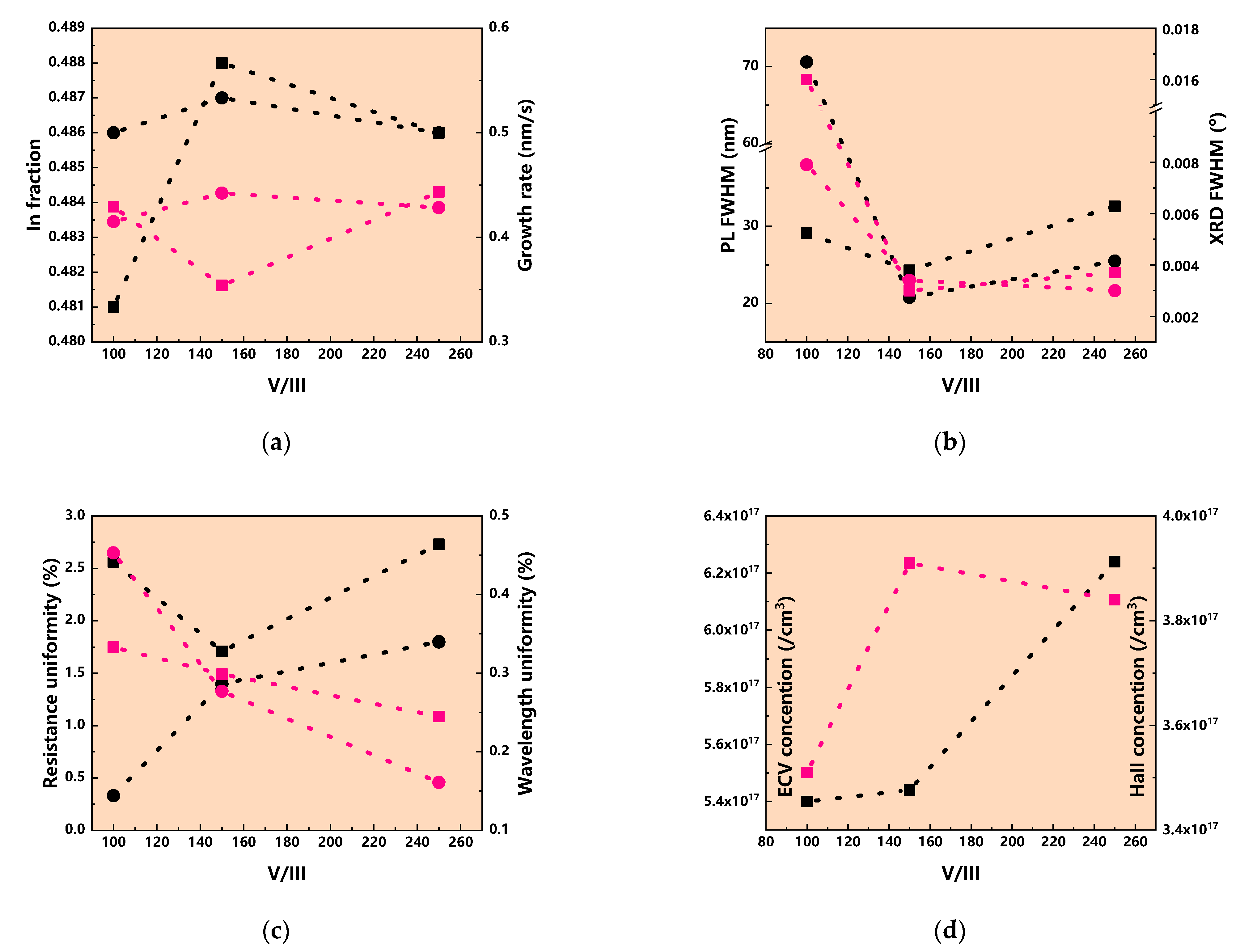
3.2. The Influence of the V/III Ratio

A series of experiments were designed to evaluate the effect of the V/III ratio on the properties of the epitaxial layers, as shown in Table 2. Sample nos. 10–12 and 13–15 was designed with a growth temperature of 600 °C and 650 °C, respectively. Sample nos. 10–15 and 16–18 was set as non-doped growth and Si-doped growth, respectively. All samples were grown at a V/III ratio ranging from 100 to 250.
Figure 2 depicts the effect of V/III on epitaxial layer characteristics. The link between the In fraction growth rate and V/III is depicted in Figure 2a. The In fraction rises first as the V/III rises. This is because as the V/III grows, so does the TMIn, which leads to an increase in the In percentage, which then remains mostly constant due to the limitations of thermal decomposition.
The relationship between the FWHM of PL spectra at room temperature and growth temperature is shown in Figure 2b. The FWHM declines initially and then climbs as the V/III increases, with a minimum of 150 at V/III. At 600 °C, the minimum FWHM is 24.3 nm, and at 650 °C, it is 20.8 nm. When the V/III ratio is less than 150, the FWHM increases significantly, and a lower V/III ratio results in a loss in crystal quality. At 600 °C, the FWHM changes slightly with the increase in the V/III, while at 650 °C, the FWHM changes significantly with the increase in the V/III. This phenomenon indicates that the low temperature case is more favorable to improving material ordering and component homogeneity. As shown in Figure 2b, the FWHM of the HRXRD diffraction peaks varies with the V/III and FWHM of PL spectra at room temperature, following a similar trend. The FWHM of the HRXRD diffraction peaks decreases abruptly with the increase in the V/III, and then remains steady. It means that when the V/III is less than 150, the crystallization quality of the InGaP epitaxial layer is largely affected by V/III, and the crystallization quality of the epitaxial layer decreases sharply as the V/III decreases. When the V/III is greater than 150, the crystallization quality of the InGaP epitaxial layer is very little affected by the V/III, and a good crystallization quality can be maintained.
Figure 2c depicts the influence of V/III on the epitaxial layer’s sheet resistance uniformity and wavelength uniformity. At 600 °C, the sheet resistance uniformity improves first, then deteriorates as the V/III increases, with the greatest sheet resistance uniformity of 1.71% at a V/III of 150. At 650 °C, the sheet resistance uniformity deteriorates as the V/III increases, with a best sheet resistance uniformity of 0.33% at a V/III of 100. As the V/III increases, wavelength uniformity improves, reaching a peak of 0.245% at 600 °C and 0.161% at 650 °C. As a result, increasing the V/III improves wavelength uniformity while decreasing resistance uniformity.
Figure 2d depicts the effect of the V/III on ECV and Hall concentrations. At 650 °C, the ECV concentration increases as the V/III increases, but the Hall concentration increases first and then decreases. The doping concentration of Si can be efficiently enhanced by the increasing V/III, primarily because Si is n-type doped and occupies Ga sites, and increasing the V/III reduces the Ga sites, which enhances the doping efficiency of Si. However, as the V/III rises from 150 to 200, the Hall concentration drops, indicating that the activation efficiency reduces at this point, a trend that is opposed to the effect of the growth temperature [19,20].

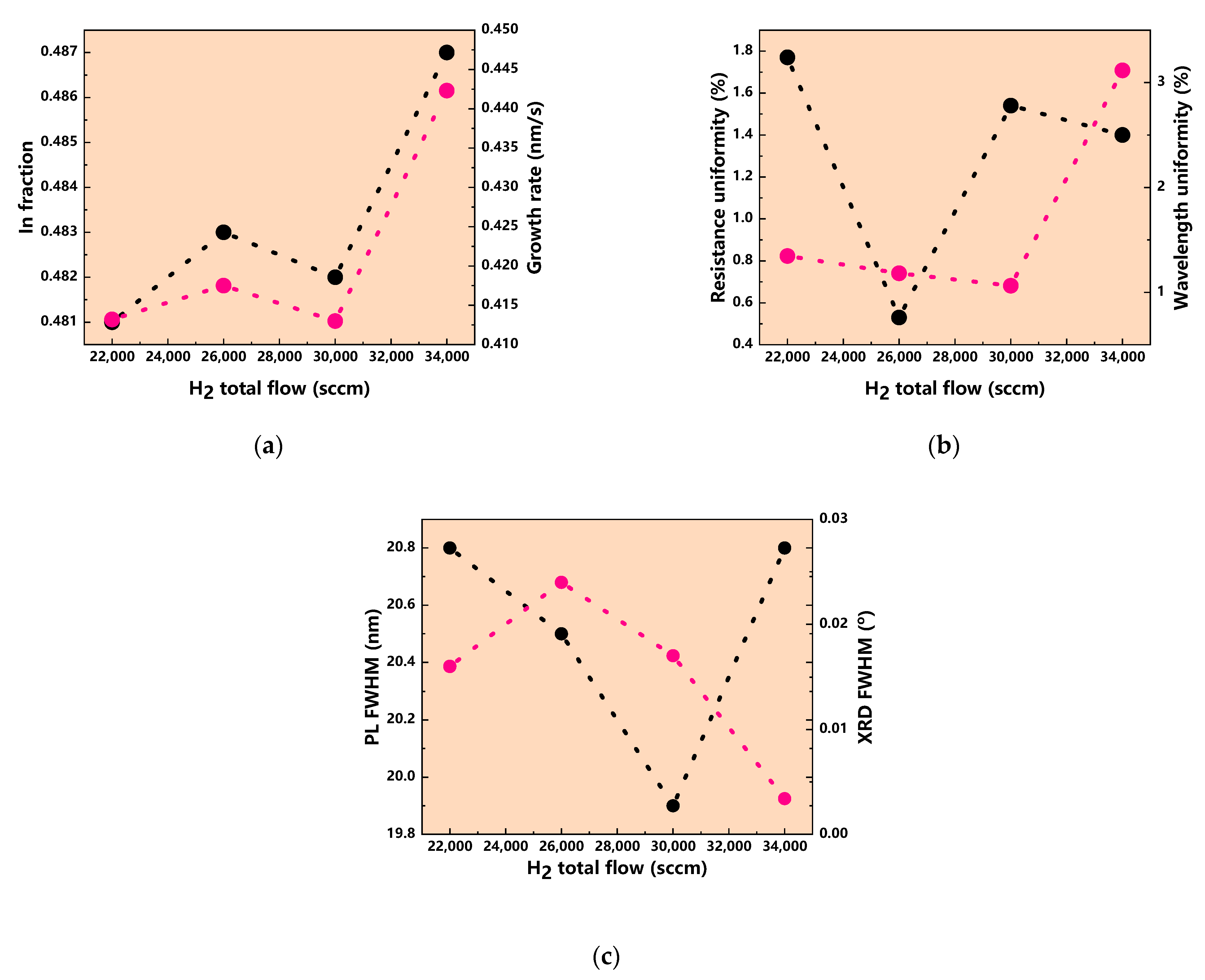
3.3. The Influence of H2 Total Flow

During the growth process, the H2 total flow has an important influence on the properties of the epitaxial layer. In turn, we investigated the effect of the H2 total flow on the epitaxial layer properties, and the corresponding growth conditions for each sample are shown in Table 3. The growth temperature and V/III ratio were set at 600 °C and 150, respectively, and the H2 total flows were 34,000 sccm, 30,000 sccm, 26,000 sccm, and 22,000 sccm, respectively.
The impact of the H2 total flow on the In fraction and growth rate is shown in Figure 3a. As seen in Figure 3a, the In fraction increases and then decreases with an overall rising trend as the H2 total flow rises. The In fraction was steadier and less influenced by the H2 total flow when it was lower than 30,000 sccm. The In fraction increases significantly when the H2 total flow increases above 30,000 sccm. As shown in Figure 3b, as the H2 total flow increases, the change in the growth rate is similar to that of the In fraction, as an increase in the H2 total flow increases the amount of the growth source passing through the growth chamber, which in turn increases the growth rate.
Figure 3b shows the influence of the H2 total flow on the epitaxial layer’s sheet resistance uniformity and wavelength uniformity. As shown in Figure 3b, as the H2 total flow increases, the sheet resistance uniformity improves and ultimately deteriorates, with the best sheet resistance uniformity of 0.53% at 26,000 sccm. When the H2 total flow is less than 30,000 sccm, the variation of square resistance uniformity with flow is severe; however, when the total H2 flow is greater than 30,000 sccm, the variation of sheet resistance uniformity with flow becomes smaller and tends to improve as the H2 total flow increases. As the H2 total flow increases, the wavelength homogeneity of the epitaxial wafer remains steady, but deteriorates significantly when the flow exceeds 30,000 sccm. The H2 total flow has a significant impact on the electrical and optical uniformity of the epitaxial layer, and controlling the H2 total flow produces an epitaxial wafer that has high electrical and optical uniformity.
Figure 3c shows the influence of the H2 total flow on the FWHM of the PL spectrum at room temperature. As shown in Figure 3c, the FWHM decreases and then increases with the increase in the H2 total flow, and the FWHM is the smallest when the H2 total flow is 30,000 sccm, which is 19.9 nm. This phenomenon indicates that the InGaP epitaxial layer has the best component uniformity when the H2 total flow is 30,000 sccm. In fact, the fluctuation range of the FWHM is 19.6 nm–20.8 nm as the H2 total flow increases from 22,000 to 34,000 sccm, so the H2 total flow has little effect on the FWHM of the PL spectrum at room temperature. Therefore, the H2 total flow has little effect on the FWHM of the PL spectrum at room temperature, and the component uniformity of the InGaP epitaxial layer is not affected by the H2 total flow.
Figure 3c also demonstrates the influence of the H2 total flow on the FWHM of the HRXRD diffraction peak. As shown in Figure 3c, with the increase in the H2 total flow, the FWHM increases and then decreases, and the minimum FWHM can be obtained at 34,000 sccm, which is 0.0034°. The smallest FWHM is 0.0034°, which indicates that the best crystallization quality of the InGaP epitaxial layer is obtained when the H2 total flow is 34,000 sccm. As the H2 total flow increases from 24,000 sccm to 34,000 sccm, the FWHM of the HRXRD diffraction peak fluctuates in the range of 0.0034°–0.017°. Therefore, the H2 total flow has a great influence on the crystalline quality of the InGaP epitaxial layer. Combined with the FWHM of the PL spectrum at room temperature analysis results, the use of a large H2 total flow is conducive to improving the material quality of the InGaP epitaxial layer.

3.4. Discussion

The processes restricting the growth rate can be divided into three primary categories according to the relationship between the growth rate and growth temperature: thermodynamics, kinetics, hydrodynamics, and mass transport. For InGaP, the growth rate is mainly limited by mass transport when the growth temperature is between 580 °C and 650 °C, and the growth rate does not change significantly with the temperature and V/III in this temperature interval. As the growth temperature increases, the In fraction decreases, mainly because TMGa requires a higher thermal decomposition temperature. The higher temperature enhances the thermal decomposition efficiency of TMGa, which in turn reduces the In fraction. The In fraction fluctuates and has some lattice mismatch with GaAs, which leads to the fluctuation of the growth rate. At the same time, due to the lattice mismatch, interfacial stresses were generated, which in turn affected the material quality and caused changes in the FWHM of the PL spectra and HRXRD diffraction peaks of the InGaP materials. The H2 total flow affects the hydrodynamics of the growth chamber and the supply of each growth source, and different growth chambers require different H2 total flows. The metal-organic chemical vapor deposition growth process is roughly divided into reaction source diffusion, thermal decomposition, adsorption, chemical reaction, surface migration, and desorption. The H2 total flow has an important effect on source diffusion during growth and the timely removal of desorption products, while a larger H2 total flow can reduce the memory effect of the growth source and produce a steep, flat interface. Our experimental results also show that a larger H2 total flow favors the uniformity of the InGaP epitaxial wafer.

4. Conclusions

We studied the impacts of temperature, the V/III ratio, and the H2 total flow on 6-in InGaP components, growth rate, uniformity, material quality, and doping efficiency in detail, and discovered the corresponding connections. The growth process is determined by gas phase diffusion in the temperature range of 600–650 °C, and the influence of temperature and V/III on the growth rate is small; at a high V/III, the variation of the In fraction with the growth temperature and V/III is small, which is beneficial to maintaining the stability of the In fraction; a high growth temperature is helpful to the improvement of epitaxial layer crystal quality, and high crystal quality can be obtained at a suitable V/III ratio; the optical and electrical uniformity of the epitaxial layer have opposite trends with the growth temperature and V/III ratio, which can be adjusted according to the actual device requirements, and the 6-in InGaP epitaxial layer with an electrical uniformity of 0.33% and optical uniformity of 0.03% was obtained in this paper; the H2 total flow has a significant impact on the electrical and optical uniformity of the epitaxial layer, and controlling the total flow of H2 enables the production of epitaxial wafers with high electrical and optical uniformity; increasing the total H2 flow can effectively improve the material quality of the InGaP epitaxial layer; and a high temperature and high V/III ratio is beneficial to improving the doping efficiency and activation efficiency of Si.

Author Contributions

Data curation, methodology, formal analysis, writing—original draft preparation, S.Y.; software, visualization, validation, Y.P.; investigation, formal analysis, W.Y.; methodology, N.G.; software, visualization, S.Z.; supervision, resources, investigation, Y.L.; project administration, investigation, supervision, Y.Z.; conceptualization, supervision, funding acquisition, writing—review and editing, X.L. All authors have read and agreed to the published version of the manuscript.

Funding

This work was supported by the Key-Area Research and Development Program of Guangdong Province (No. 2021B0101300001), The Youth Innovation Promotion Association of Chinese Academy of Sciences (Grant No. 2015094).

Data Availability Statement

The data that support the findings of this study are available from the corresponding authors, Y.Z. and X.L., upon reasonable request.

Conflicts of Interest

The authors declare no conflict of interest.

References

  1. Ju, I.; Lee, S.; Cressler, J.D. An Efficient, Broadband SiGe HBT Non-Uniform Distributed Power Amplifier Leveraging a Compact, Two-Section λ/4 Output I\mpedance Transformer. IEEE Trans. Microw. Theory Tech. 2022, 70, 3524–3533. [Google Scholar] [CrossRef]
  2. Kopytko, M.; Rogalski, A. Figure of Merit for Infrared Detector Materials. Infrared Phys. Technol. 2022, 122, 104063. [Google Scholar] [CrossRef]
  3. Sun, T.; Yang, K.; Wei, J.; Jia, Y.; Deng, S.; Zhao, Z.; Zhang, B.; Luo, X. High-Voltage Polarization-Superjunction GaN HEMT With Built-In SBD for Low Reverse Conduction Loss. IEEE J. Electron Devices Soc. 2022, 10, 808–812. [Google Scholar] [CrossRef]
  4. Pan, G.; Xun, M.; Sun, Y.; Zhao, Z.; Xu, C.; Xie, Y.; Wu, D.; Zhou, J. Two-Dimensional Coherent VCSEL Arrays with Configurable Beam Emissions. Opt. Laser Technol. 2022, 149, 107809. [Google Scholar] [CrossRef]
  5. Cho, I.-W.; Park, S.H.; Nguyen, T.T.; Kim, Y.; Lee, S.J.; Ryu, M.-Y. Effect of Tunnel Junction Grown at Different Growth Rates on the Optical Properties and Improved Efficiency of InGaP/GaAs Double-Junction Solar Cells. J. Alloys Compd. 2020, 832, 154989. [Google Scholar] [CrossRef]
  6. Gou, Y.; Wang, H.; Wang, J.; Yang, H.; Deng, G. High Performance P++-AlGaAs/N++-InGaP Tunnel Junctions for Ultra-High Concentration Photovoltaics. Optics Express 2022, 30, 23763. [Google Scholar] [CrossRef]
  7. Mao, Q.; Huang, L.; Xiang, Z.; Zhu, D.; Meng, J. High-Power Microwave Pulse Induced Failure on InGaP/GaAs Heterojunction Bipolar Transistor. Microelectron. Reliab. 2022, 139, 114848. [Google Scholar] [CrossRef]
  8. Sodabanlu, H.; Ubukata, A.; Watanabe, K.; Sugaya, T.; Nakano, Y.; Sugiyama, M. High-Speed MOVPE Growth of InGaP Solar Cells. IEEE J. Photovolt. 2020, 10, 480–486. [Google Scholar] [CrossRef]
  9. Ha, S.T.; Paniagua-Domínguez, R.; Kuznetsov, A.I. Room-Temperature Multi-Beam, Multi-Wavelength Bound States in the Continuum Laser. Adv. Opt. Mater. 2022, 10, 2200753. [Google Scholar] [CrossRef]
  10. Cho, I.-W.; Ryu, M.-Y.; Song, J.D. Temperature-Dependent Carrier Dynamics of InP/InGaP Quantum Structures Grown at Various Growth Temperatures Using Migration-Enhanced Epitaxy. J. Lumin. 2020, 223, 117214. [Google Scholar] [CrossRef]
  11. Peng, C.-Y.; Huang, W.-T.; Lu, Z.-K.; Chen, S.-C.; Kuo, H.-C. Design of High-Power Red VCSEL on a Removable Substrate. Photonics 2022, 9, 763. [Google Scholar] [CrossRef]
  12. Wang, L.; King, I.; Chen, P.; Bates, M.; Lunt, R.R. Epitaxial and Quasiepitaxial Growth of Halide Perovskites: New Routes to High End Optoelectronics. APL Mater. 2020, 8, 100904. [Google Scholar] [CrossRef]
  13. Gomyo, A.; Suzuki, T.; Kobayashi, K.; Kawata, S.; Hino, I.; Yuasa, T. Evidence for the Existence of an Ordered State in Ga0.5In0.5P Grown by Metalorganic Vapor Phase Epitaxy and Its Relation to Band-Gap Energy. Appl. Phys. Lett. 1987, 50, 673–675. [Google Scholar] [CrossRef]
  14. Sangiovanni, D.G.; Faccio, R.; Gueorguiev, G.K.; Kakanakova-Georgieva, A. Discovering Atomistic Pathways for Supply of Metal Atoms from Methyl-Based Precursors to Graphene Surface. Phys. Chem. Chem. Phys. 2023, 25, 829–837. [Google Scholar] [CrossRef]
  15. Kakanakova-Georgieva, A.; Ivanov, I.G.; Suwannaharn, N.; Hsu, C.-W.; Cora, I.; Pécz, B.; Giannazzo, F.; Sangiovanni, D.G.; Gueorguiev, G.K. MOCVD of AlN on Epitaxial Graphene at Extreme Temperatures. Catal. Sci. Technol. 2021, 23, 385–390. [Google Scholar] [CrossRef]
  16. Liu, Z.; Zhu, H.; Pan, X.; Huang, Y. Burn-in Effect in InGaP/GaAs HBT with Intrinsically or Extrinsically Carbon Doped Base Layer. Phys. Scr. 2023, 98, 065009. [Google Scholar] [CrossRef]
  17. Elhamri, S.; Ahoujja, M.; Newrock, R.S.; Mast, D.B.; Herbert, S.T.; Mitchel, W.C.; Razeghi, M. Electrical Properties of Undoped GaxIn1−xP/GaAs Quantum Wells. Phys. Rev. B 1996, 54, 10688–10695. [Google Scholar] [CrossRef]
  18. Heidelberger, C.; Fitzgerald, E.A. GaAsP/InGaP Heterojunction Bipolar Transistors Grown by MOCVD. J. Appl. Phys. 2017, 121, 045703. [Google Scholar] [CrossRef] [Green Version]
  19. Forghani, K.; Reddy, R.; Rowell, D.; Tatavarti, R. MOVPE Growth of AlInP–InGaP Distributed Bragg Reflectors. IEEE J. Photovolt. 2020, 10, 754–757. [Google Scholar] [CrossRef]
  20. Kınacı, B.; Özen, Y.; Kızılkaya, K.; Asar, T.; Çetin, S.Ş.; Boyalı, E.; Öztürk, M.K.; Memmedli, T.; Özçelik, S. Effect of Alloy Composition on Structural, Optical and Morphological Properties and Electrical Characteristics of GaxIn1−xP/GaAs Structure. J. Mater. Sci. Mater. Electron. 2013, 24, 1375–1381. [Google Scholar] [CrossRef]
  21. Attolini, G.; Bocchi, C.; Germini, F.; Pelosi, C.; Parisini, A.; Tarricone, L.; Kùdela, R.; Hasenohrl, S. Effects of Inhomogeneities and Ordering in InGaP/GaAs System Grown by MOVPE. Mater. Chem. Phys. 2000, 66, 246–252. [Google Scholar] [CrossRef]
  22. Pitts, O.J.; Benyon, W.; SpringThorpe, A.J. Modeling and Process Control of MOCVD Growth of InAlGaAs MQW Structures on InP. J. Cryst. Growth 2014, 393, 81–84. [Google Scholar] [CrossRef]
  23. Jakomin, R.; Parisini, A.; Tarricone, L.; Longo, M.; Fraboni, B.; Vantaggio, S. On the Electrical Properties of Si-Doped InGaP Layers Grown by Low Pressure-metalorganic Vapor Phase Epitaxy. Thin Solid Film. 2012, 520, 6619–6625. [Google Scholar] [CrossRef]
  24. Hageman, P.R.; van Geelen, A.; Gabriëlse, W.; Bauhuis, G.J.; Giling, L.J. Optical and Electrical Quality of InGaP Grown on GaAs with Low Pressure Metalorganic Chemical Vapour Deposition. J. Cryst. Growth 1992, 125, 336–346. [Google Scholar] [CrossRef]
  25. Martín, G.; Coll, C.; López-Conesa, L.; Rebled, J.M.; Barrigón, E.; García, I.; Rey-Stolle, I.; Algora, C.; Cornet, A.; Estradé, S.; et al. Understanding the Anisotropy in the Electrical Conductivity of CuPt B -Type Ordered GaInP Thin Films by Combining In Situ TEM Biasing and First Principles Calculations. ACS Appl. Electron. Mater. 2022, 4, 3478–3485. [Google Scholar] [CrossRef]
Figure 1. The impact of growth temperature on various properties of the epitaxial layer. Circular marks represent a V/III ratio of 250, while square marks correspond to a V/III ratio of 100. (a) Shows the effects of growth temperature on the In fraction (black) and the growth rate (red). (b) Demonstrates the influence of growth temperature on the FWHM of the PL spectrum at room temperature (black) and the FWHM of HRXRD diffraction peak (red). (c) Presents the influence of growth temperature on the uniformity of the sheet resistance (black) and the uniformity of the luminous wavelength (red). Finally, (d) depicts the influence of growth temperature on ECV doping concentration (black) and Hall concentration (red).
Crystals 13 01165 g001
Figure 2. The impact of V/III ratio on various properties of epitaxial layer. Circular marks represent growth temperature of 600 °C, while square marks correspond to growth temperature of 650 °C. (a) Shows the effects of V/III ratio on the In fraction (black) and the growth rate (red). (b) Demonstrates the influence of V/III ratio on the FWHM of the PL spectrum at room temperature (black) and the FWHM of HRXRD diffraction peak (red). (c) Presents the influence of V/III ratio on the uniformity of the sheet resistance (black) and the uniformity of the luminous wavelength (red). Finally, (d) shows the influence of V/III ratio on ECV doping concentration (black) and Hall concentration (red).
Crystals 13 01165 g002
Figure 3. The impact of H2 total flow on various properties of the epitaxial layer. (a) Shows the effects on the In fraction (black) and the growth rate (red). (b) Presents the influence of H2 total flow on the uniformity of the sheet resistance (black) and the uniformity of the luminous wavelength (red). (c) Demonstrates the influence of H2 total flow on the FWHM of the PL spectrum at room temperature (black) and the FWHM of HRXRD diffraction peak (red).
Crystals 13 01165 g003
Table 1. Explore the influence of growth temperature on the properties of the epitaxial layer, the corresponding temperature, V/III, and the Si2H6 flow of each sample.
No.Growth TemperatureV/IIISi2H6 Flow
1580 °C2500 sccm
2600 °C2500 sccm
3650 °C2500 sccm
4580 °C1000 sccm
5600 °C1000 sccm
6650 °C1000 sccm
7580 °C1001.3 sccm
8600 °C1001.3 sccm
9650 °C1001.3 sccm
Table 2. Exploration into the influence of V/III ratio on the properties of the epitaxial layer, the corresponding temperature, V/III, and the Si2H6 flow of each sample.
No.Growth TemperatureV/IIISi2H6 Flow
10600 °C1000 sccm
11600 °C1500 sccm
12600 °C2500 sccm
13650 °C1000 sccm
14650 °C1500 sccm
15650 °C2500 sccm
16650 °C1001.3 sccm
17650 °C1501.3 sccm
18650 °C2501.3 sccm
Table 3. Investigation of the effect of the H2 total flow on epitaxial layer characteristics. Each sample’s H2 total flow, growth temperature, and V/III ratio.
No.H2 Total FlowGrowth TemperatureV/III
1934,000 sccm600 °C150
2030,000 sccm600 °C150
2126,000 sccm600 °C150
2222,000 sccm600 °C150
Disclaimer/Publisher’s Note: The statements, opinions and data contained in all publications are solely those of the individual author(s) and contributor(s) and not of MDPI and/or the editor(s). MDPI and/or the editor(s) disclaim responsibility for any injury to people or property resulting from any ideas, methods, instructions or products referred to in the content.

