Abstract
In this study, we used a horizontal hot-wall CVD epitaxy apparatus to grow epitaxial layers on 4° off-axis 4H-SiC substrates. Epitaxial films were grown by adjusting the flow rate of the source gas at different levels. With an increase in the source gas flow rate, a notable transition in the crystalline structure of the epitaxial layer was observed, gradually shifting from 4H-SiC to 3C-SiC. Furthermore, the quality of the epitaxial layer correspondingly exhibited degradation. Specifically, for epitaxial films grown under moderate gas flow rates, the central region demonstrated a crystalline structure of 4H-SiC, while the outer ring region exhibited a crystalline structure of 3C-SiC. Using a scanning electron microscope (SEM) to observe the transition zone of the two regions, a region of 3C/4H overlapping growth below it was found. Bright areas corresponded to 3C, while dark areas corresponded to 4H, as confirmed by Raman spectroscopy and other SEM images. The growth interfaces of the two crystal types were clearly discernible and relatively compact. Furthermore, the growth angles of the two crystal types and their correlation with the cutting direction strongly suggest that this overlap is related to the formation of micro-nano steps on the substrate surface.
1. Introduction
The advent of power electronics in the new era relies on the emergence of wide-bandgap semiconductor materials. Among these materials, Silicon Carbide (SiC), particularly in its 4H-SiC form, stands out as a representative third-generation semiconductor [1,2,3]. Notably, SiC boasts a bandgap width three times wider than that of silicon (Si) and a critical breakdown electric field ten times greater than Si. These inherent characteristics endow SiC-based devices with superior performance in terms of voltage handling, power capacity, and operational frequency [4]. Furthermore, 4H-SiC demonstrates an elevated electron saturation drift velocity and superior thermal conductivity, rendering SiC power electronic devices highly advantageous in high-temperature and high-power applications [5,6]. The wide bandgap width, high critical breakdown electric field, elevated electron saturation drift velocity, excellent thermal conductivity, and remarkable physical and chemical stability of SiC provide ample opportunities for optimizing SiC power devices, especially with respect to device dimensions, quality, operating temperature, and switching losses. Among the various polytypes of SiC, cubic silicon carbide (3C-SiC) has emerged as a highly promising candidate due to its bandgap of 2.36 eV [7]. This polytype exhibits exceptional physical characteristics, including high electron mobility, drift velocity, and low interface trap density, distinguishing it from other SiC polytypes and traditional semiconductors [8]. The diverse crystal structures within the same material showcase remarkable properties in distinct domains, underscoring the immense application potential of SiC materials [9]. Consequently, research studies on SiC have garnered significant attention from the global scientific community.
Silicon Carbide (SiC) exhibits two polar surfaces in its hexagonal form, namely and , and two polar surfaces in its cubic form, namely and [1]. Of particular interest is the growth of 3C/4H-SiC on the carbon face due to the presence of polarization-induced bound charges and significant differences in the conduction band at the 3C/4H interface [10,11,12]. This configuration is expected to result in a higher concentration of two-dimensional electron gas (2DEG) at the 3C/4H-SiC interface [13], offering promising prospects for MOSFET structures [7]. Since 3C and 4H SiC belong to the same material, there are no compositional fluctuations or alloy scattering effects [14]. Moreover, the nearly identical lattice constants of 3C and 4H SiC contribute to a reduced degree of lattice mismatch and subsequent interface defects [15,16]. These characteristics enable the utilization of bulk 3C material for the formation of high-speed channels [17,18]. Furthermore, both crystal structures of SiC, 3C, and 4H exhibit similar thermal expansion coefficients [19,20] and possess excellent heat dissipation capabilities, ensuring high reliability in device fabrication [21].
Coaxial hexagonal SiC substrates are commonly employed for the growth of 3C-SiC layers. In this configuration, 3C-SiC typically undergoes two-dimensional nucleation on the substrate surface. It is well-established that 3C-SiC exhibits two rotational domain types, namely ABC… and ACB…, which tend to form double positioning boundaries (DPB defects) [22]. These defects propagate to the surface, giving rise to macroscopic defects. Previous research has focused on growing 3C-SiC on 4H-SiC using various techniques, including chemical vapor deposition (CVD) [23,24,25], solution growth [26], vapor–liquid–solid (VLS) methods [27], and sublimation methods [28]. However, most of these studies have primarily concentrated on the growth of 3C-SiC on the Si face, resulting in limited single-layer growth. Consequently, the 3C/4H composite structures grown in these investigations did not exhibit a high concentration of two-dimensional electron gas. In alternative studies, researchers opted to directly grow 3C-SiC on the C face of 4H-SiC [29]. Nevertheless, due to the limited amount of research and the relative immaturity of the growth processes, the quality of 3C-SiC grown on the C face remains relatively poor.
The 4H-SiC crystal exhibits two prominent characteristic peaks, namely the FLO peak at 965.3 and the FTO peak at 777.0 . Additionally, a relatively faint peak is observed at 798.2 . In contrast, the 3C-SiC crystal displays distinct features with the FLO peak positioned at 973.5 and the FTO peak at 798.2 . Notably, no discernible peak is observed at 777.0 for 3C-SiC [30]. When employing Raman spectroscopy to discriminate between these two distinct SiC crystal structures, the close proximity of their peak positions renders the FLO peak less suitable as a definitive criterion. Instead, the positions of the FTO peak in the Raman spectra are conventionally selected to distinguish between the two crystal structures [9,10].
For the present paper, we conducted a study on the epitaxial growth of a layered structure consisting of 3C/4H-SiC on the Si face of 4H-SiC. Our approach capitalized on well-established epitaxial growth processes that have reached a mature stage of development. By implementing this layered epitaxy, a well-defined interface between 3C-SiC and the C face of 4H-SiC is attainable. Previous studies have indicated that this interface can exhibit a high concentration of two-dimensional electron gas (2DEG). Additionally, due to the layered epitaxial structure, multiple interfaces are present within the epitaxial layer, enabling the concurrent fabrication of multiple channels during a single growth process. This feature significantly enhances the overall mobility of the channels and improves the gate control capability over these channels. Overall, our research explores the potential of layered epitaxy for growing 3C/4H-SiC structures on 4H-SiC substrates, leveraging the advantages of both crystal structures. Both the formation of a high concentration of 2DEG at the 3C/4H interface and the simultaneous fabrication of multiple channels offer promising prospects for achieving high-performance SiC-based power electronic devices.
2. Experiment
In order to achieve high-quality epitaxy, step control was employed by creating regular micro-nano steps with specific height variations on the surface of the epitaxial wafer [31]. During the epitaxial growth process, these steps on the substrate surface serve as templates for the attachment and growth of surface source gas molecules, resulting in the formation of high-quality epitaxial films. In this study, SiC epitaxial films were grown on 4H-SiC substrates using a chemical vapor deposition (CVD) system. A hot-wall CVD reactor with H2-diluted Cl3HSi (TCS) and C2H4 precursors was utilized. The growth process was performed on a 6-inch n-type 4H-SiC wafer with a Si surface. Prior to growth, the surface was meticulously cleaned using acetone, ethanol, and deionized water. The SiC substrate was then heated from room temperature to 1570 °C within 34 min under a flow rate of 100 slm H2. Subsequently, the temperature and gas flow rate were maintained while etching the surface for 4 min to create the desired micro-nano steps. To initiate growth, a TCS flow rate of 27 sccm was introduced as the Si source, and C2H4 with a flow rate of 8 sccm served as the C source. A C/Si ratio of 0.59 was maintained through precise control of the precursor flow. Additionally, N2 gas was introduced at a total flow rate of 65 sccm for doping purposes. This process lasted for 8 min, resulting in the growth of a buffer layer on the substrate surface. Subsequently, with the H2 flow rate and temperature held constant, the target epitaxial layer with a thickness of 10 μm was grown. The same C source and Si source were used, and the C/Si ratio was maintained at 0.72 by adjusting the precursor flow. N2 gas was introduced for N-type doping during the growth of the final target epitaxial layer. During the final stage of epitaxial growth, we conducted experiments to investigate the relationship between the growth rate and source gas flow rate. Specifically, we performed epitaxial growth experiments under three distinct source gas flow conditions: low, medium, and high. To achieve this, we adjusted the flow rate of TCS to 50 sccm, 75 sccm, and 100 sccm, respectively, while maintaining consistent proportions of C2H4 and N2 flow rates. These experimental conditions resulted in three sets of samples, labeled as sample 1, sample 2, and sample 3. Additionally, to ensure that an equivalent total gas volume entered the chamber for all three sets of epitaxial films, the growth times for the final step were set to 36 min, 25 min, and 18 min, respectively.
3. Results and Discussion
Figure 1 depicts the surface morphology of the three epitaxial samples. Figure 1a–c show the central region of sample 1, sample 2, and sample 3, respectively, while Figure 1d–f represent the outer region of each respective sample. In Figure 1a,d, the central and outer regions of sample 1 exhibit a uniform appearance, featuring a smooth and bright surface without noticeable defects. Similarly, in Figure 1c,f, the central and outer regions of sample 3 display consistent characteristics, showcasing a rough and grayish surface. However, Figure 1b,e reveal distinctive features in the central and outer regions of sample 2. Sample 2 can be divided into two regions: a central smooth region (Figure 1b) and an outer rough annular region (Figure 1e). The central smooth region shares similarities with sample 1, displaying a smooth and bright mirror-like surface with no apparent defects. In contrast, the outer rough annular region resembles the surface of sample 3, exhibiting a rough and grayish appearance.
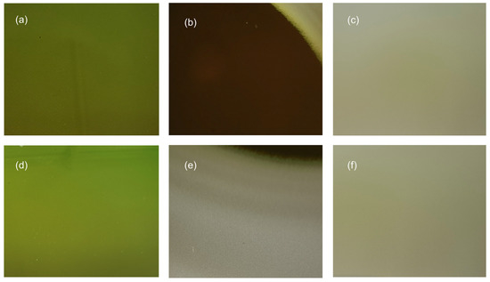
Figure 1.
Photographs of epitaxial wafers: (a–c) the central region of sample 1, sample 2, and sample 3; (d–f) the outer region of sample 1, sample 2, and sample 3.
Figure 2 illustrates the optical microscope images of different regions of the three epitaxial samples. Figure 2a displays the optical microscope image of sample 1, revealing a smooth and flat surface without notable undulations. However, a few triangular defects caused by debris are visible on the surface, as depicted in Figure 2b. Figure 2f showcases the optical microscope image of the surface of sample 3, demonstrating a rough and complex polycrystalline morphology, indicative of poor epitaxial quality. Figure 2c captures the image of the central smooth region of sample 2, which appears smooth and bright under the optical microscope. The surface morphology of the central smooth region of sample 2 exhibits no discernible differences compared to sample 1. In contrast, Figure 2d presents the image of the outer rough annular region of sample 2. Notably, the proportion of flat plateau-like regions on the surface is significantly higher compared to sample 3. Additionally, the surface displays uneven islands with varying heights. Figure 2e reveals the surface morphology of the transitional region between the central smooth region and the outer rough annular region of sample 2. Evidently, elongated step-like features begin to emerge on the surface, extending radially.
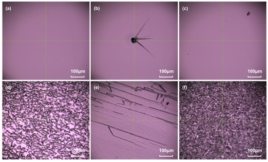
Figure 2.
Optical microscope images depicting distinct regions of the three epitaxial wafers: (a) surface of sample 1; (b) triangular defects on the surface of sample 1; (c) the centrally smooth region on the surface of sample 2; (d) the outer rough annular region of sample 2; (e) the surface morphology of the transitional region between the centrally smooth region and the outer rough annular region of sample 2; (f) surface of sample 3.
A more detailed examination of different regions of the three samples was conducted using a SEM. Figure 3a illustrates the surface morphology of sample 1 at a magnification of 600×, revealing a triangular defect caused by debris. The size of the triangular defect is considerable, reaching the scale of hundreds of micrometers. To further analyze the defect, we investigated the regions near the defect bottom and defect-free areas at higher magnifications. Figure 3b presents the image near the bottom of the defect at a magnification of 20,000×. Fine steps extending along the bottom of the triangular defect on the epitaxial surface can be observed. In contrast, the surface without any debris influence, as depicted in Figure 3c, remains smooth and flat even under high-magnification SEM observation, exhibiting no noticeable growth defects. Figure 3d–f display SEM images of sample 3’s surface at magnifications of 1300×, 5000×, and 20,000×, respectively. The surface of sample 3 reveals small and discontinuous plateau regions. The sample exhibits high-density and deep tubular defects, which are speculated to arise from boundaries between multiple different domain regions where external gas molecules encounter difficulty in penetrating and completing encapsulation. Some tubular defects feature larger apertures on the surface, while others exhibit triangular or elongated shapes. Notably, noticeable height variations in the form of steps can be observed surrounding the tubular defects. The epitaxial growth of SiC around these tubular defects appears discontinuous, resulting in a fragmented polycrystalline appearance.
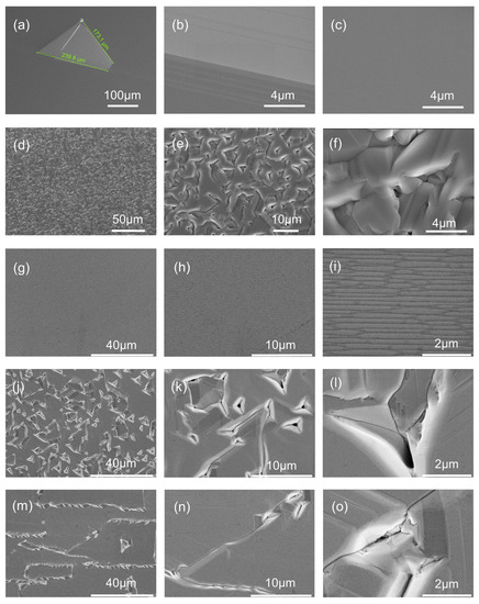
Figure 3.
SEM images of different regions of the three epitaxial wafers: (a–c) surface of sample 1; (d–f) surface of sample 3; (g–i) surface of the centrally smooth region on the surface of sample 2; (j–l) the outer rough annular region of sample 2; (m–o) the surface morphology of the transitional region between the centrally smooth region and the outer rough annular region of sample 2.
Figure 3g–i present SEM images of the central region of sample 2 at different magnifications. The surface exhibits a smooth and bright appearance under optical microscopy, but a noticeable accumulation of steps can be observed. In comparison to the surface morphology observed in Figure 3c for sample 1, it is evident that the epitaxial growth quality of sample 2 of the central flat region is noticeably inferior when compared to the epitaxial growth of sample conducted under low-source gas flow conditions.
Figure 3j–l illustrate SEM images of the rough outer ring region of sample 2 at different magnifications. In comparison to the surface of sample 3 shown in Figure 3d–f, a larger proportion of plateau regions is observed on the surface of sample 2. The area surrounding the exit of tubular defects exhibits triangular pits instead of distinct step height variations. Each defect is connected to two or three DPB defects, forming V-shaped grooves along the DPB defects on the surface. The growth quality is superior to that of the epitaxial sample grown under high source gas flow (sample 3). Figure 3m–o display the transitional region between the central smooth region and the rough outer ring area of sample 2. This region exhibits characteristics of both the central smooth region and the rough outer ring region. It is predominantly composed of connected plateau regions resembling the features of the central smooth region. However, a small number of DPB defects are present on the surface, and at the intersections of different DPB defects, a few tubular defects can be observed. This characteristic is similar to the rough outer ring region. Notably, just below this rough region, a layered stacking structure of interest is present.
In order to test the crystal structure of the epitaxial layer, we performed Raman measurements on different regions of the surfaces of three epitaxial samples and the substrate, as shown in Figure 4. Due to the thin thickness of the epitaxial layer (only 10 μm), the penetration depth of the laser spot exceeded 10 μm, resulting in the Raman signal containing contributions from the substrate. When comparing the Raman spectra of the central flat regions in sample 1 and sample 2, using the Raman peaks of the substrate as a reference, the presence of the characteristic peak of 4H-SiC at 777 indicated that the crystal structure in that region was the same as the substrate, predominantly 4H-SiC. The peaks near 977 coincided with the peaks on the substrate and could be attributed to the Raman signal from the substrate. In contrast, the Raman signal from the outer ring-shaped rough region of sample 3 and sample 2 exhibited not only the 4H feature peak near 777 similar to the substrate but also a distinct feature peak belonging to 3C-SiC at 797 . Furthermore, the characteristic peak appearing near 972 , compared to the corresponding peak on the substrate, was closer to the FLO peak of 3C-SiC. These data indicated that the epitaxial layer in the outer ring-shaped rough region of sample 3 and sample 2 was composed of 3C-SiC. We conducted a cross-sectional SEM analysis on sample 2. Figure 5a shows the SEM image of the cross-section of the outer ring-shaped rough region corresponding to the 3C-SiC region. From the SEM image, it is evident that the epitaxial layer (3C-SiC) and the substrate (4H-SiC) exhibited distinct differences in their crystal structure. The 3C-SiC epitaxial layer appeared brighter in the SEM image and had a clear demarcation line with the substrate (4H-SiC). In contrast, when the crystal structure of the epitaxial layer was 4H-SiC, as shown in Figure 5b, there was no apparent contrast at the interface with the substrate. This difference in contrast at the interface served as an important criterion for determining the SiC crystal structure in the SEM images.
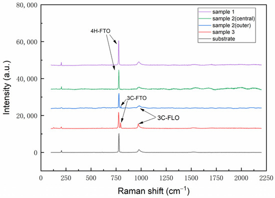
Figure 4.
The Raman spectra of different regions of the three epitaxial wafers and the substrate.
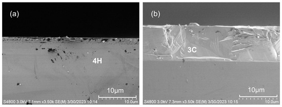
Figure 5.
SEM images of the cross-section of different regions of sample 2: (a) the central flat region, the 4H-SiC region; (b) the outer rough region, the 3C-SiC region.
Figure 6a,b present typical cross-sectional SEM images of the transition region in sample 2, revealing a layered growth of 3C/4H-SiC along the direction. Herein, we refer to the cross-section shown in Figure 6a as section A. In section A, the thickness of the monolayer 3C/4H-SiC is basically about 0.3 μm, and the angle formed between each monolayer and the substrate is about 4°. The displayed cross-section in the image contains approximately seven layers, with each layer extending from the substrate to the upper 3C-SiC layer. Within each layer, there is a uniform variation in crystal structure. The crystal structure gradually transitions from 4H-SiC near the substrate to 3C-SiC near the surface of the epitaxial layer. However, the rate of variation between adjacent layers differs, leading to a distinct boundary between 3C/4H-SiC in the middle region. We refer to the section shown in Figure 6a as section B. In Figure 6b, the overlaid epitaxial layer grows parallel to the substrate. The observed angle difference is due to the difference in crystal orientation along the cross-sectional direction, which will be explained in conjunction with Figure 7. The V-shaped grooves on the epitaxial surface mainly appear on the outer surface of 3C-SiC and do not significantly affect the overlaid growth region. The crystal quality of the epitaxial growth is good. In this structure, there are multiple 3C/4H heterostructures, with the C-face of 4H-SiC being the interface. Previous research has indicated a high concentration of 2EDG at the interface between the C-face of 4H-SiC and 3C-SiC. The presence of this 3C/4H layered structure holds promise for the fabrication of multi-channel MOSFETs.
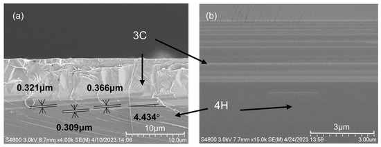
Figure 6.
SEM images of the cross-section of the transitional region between the centrally smooth region and the outer rough annular region of sample 2: (a) section A; (b) section B.
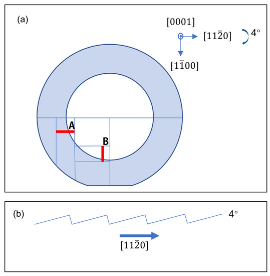
Figure 7.
(a) The position of the section A and B. (b) Micro-nano steps on the substrate surface along the direction.
Figure 7a presents a schematic illustration depicting the cross-section of Figure 6 on the epitaxial wafer. The labels A and B correspond to section A and section B, respectively. By tilting the substrate at an angle of 4° along the direction, the surface of the substrate exhibits alternating steps along the same direction, as illustrated in Figure 7b. These steps on the substrate serve as templates for epitaxial growth during the process. Consequently, in the cross-sectional view of the epitaxial layer along the direction, an inclination angle between the 3C/4H-SiC epitaxial layer and the substrate can be observed. Conversely, along the direction, the step on the substrate extends infinitely. Consequently, when the epitaxial wafer is cut in this direction, the cross-section of the epitaxial layer becomes parallel to the substrate. These distinct cross-sectional views obtained through cutting along different directions provide compelling evidence for the impact of micro-nano steps on the substrate surface, which plays a significant role in constraining the layered epitaxial growth process.
Figure 8 presents atomic force microscopy (AFM) images of the epitaxial layer in sample 2. Specifically, Figure 8a depicts the AFM image captured from the center flat region of sample 2, which provides evidence of distinct step bunching on the surface. Figure 8b demonstrates the extension of the step bunching observed in the center flat region into the transition region. Within this transition region, the steps undergo a process of widening and height increase. Subsequently, the widened steps align in a direction parallel to the substrate surface, forming a platform-like structure. Notably, the step bunching originating from the center flat region terminates precisely at the edge of this platform structure.
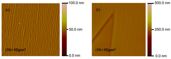
Figure 8.
AFM images of different regions on the surface of sample 2: (a) the central flat region; (b) the transitional region.
From the obtained data, it is evident that, under high-growth-rate conditions with increased source gas flow, the epitaxial layer exhibits a 3C crystal structure, whereas, under low-growth-rate conditions with reduced source gas flow, the epitaxial layer adopts a 4H crystal structure. These observations can be elucidated through the utilization of two distinct growth modes: two-dimensional nucleation and step flow. Theoretical considerations such as the BCF theory [32] highlight the pivotal role of the maximum supersaturation on the step surfaces relative to the critical supersaturation in dictating the nucleation mechanism during epitaxial growth. Specifically, at low growth rates and diminished source gas flow, the modest source gas concentration yields < , promoting step flow growth. Herein, the epitaxial layer progresses by aligning with the underlying substrate’s steps, ensuring consistent 4H crystal structure alignment between the epitaxial layer and substrate. In contrast, high-growth-rate conditions accompanied by elevated source gas flow induce heightened source gas concentration. Consequently, surpasses , thereby facilitating two-dimensional nucleation growth and the subsequent emergence of a distinct 3C crystal structure, which deviates from the underlying substrate’s crystal structure. Meanwhile, when the growth rate assumes a medium value, i.e., 1.5 times the source gas flow rate, the source gas concentration precisely corresponds to a critical threshold. Under these circumstances, the epitaxial layer’s crystal structure is influenced by additional minor factors. The experimental apparatus employed for epitaxial growth, depicted in Figure 9, entails the rotation of the substrate under the influence of gas flow, fostering the growth of the epitaxial layer. During traversal through the peripheral region of the epitaxial wafer, the source gas encounters heightened concentration levels, thereby promoting growth via two-dimensional nucleation. Consequently, a 3C crystal structure is formed, albeit exhibiting inferior growth quality. The continuous rotation of the wafer engenders a uniformly roughened peripheral surface, which is attributed to the growth in the outer region. As the gas progresses beyond the outer region, its concentration diminishes, consequently leading to a shift in growth conditions. Upon reaching the central region, the supersaturation levels shift, manifesting as < , thereby reinstating step flow growth and ensuring consistency with the underlying substrate’s crystal structure, i.e., 4H. When the gas concentration is situated at the boundary between the rough outer ring and the central flat region, it coincides with the critical point required for both step-flow and two-dimensional nucleation growth. At this juncture, the gas concentration is conducive to epitaxial growth. Upon attachment to the substrate surface, gas molecules exhibit weak binding. Subsequently, these molecules may migrate towards either of the adjacent steps and adhere to their surfaces. Unlike step-flow growth, which relies on the presence of step edges, two-dimensional nucleation growth permits nucleation to transpire at the center of the step. Consequently, two-dimensional nucleation offers a greater number of growth points and accommodates a higher influx of gas molecules within a given timeframe. Moreover, the consumption of gas concentration is heightened during two-dimensional nucleation growth. Under normal circumstances, the disparity in gas consumption rate between step-flow and two-dimensional nucleation growth is minor and does not influence the crystal structure of the surrounding growth. However, at this critical juncture, the gas concentration aligns with the critical gas concentration necessary for both step-flow and two-dimensional nucleation growth. Assuming a constant concentration of gas molecules attached to the surface of a given area, the increased consumption of gas molecules during two-dimensional nucleation growth results in a diminished gas concentration available for the adjacent area to satisfy the conditions for step-flow growth. Consequently, the crystal structure of the growth in that region assumes a 4H configuration. Conversely, step-flow growth curtails gas molecule consumption, leaving a surplus of gas molecules available for the next adjacent area. This surplus satisfies the requirements for two-dimensional nucleation growth, leading to the crystal structure of 3C. This periodic variation in surface concentration perpetuates the gas concentration in proximity to the critical value, thereby facilitating the periodic 3C/4H-SiC epitaxial growth. Additionally, as the crystal structure tends to align with the substrate within the same layer, the periodic variation in crystal structure within a given layer gradually expands as the steps of the epitaxial layer proliferate, ultimately engendering a layered epitaxial structure.
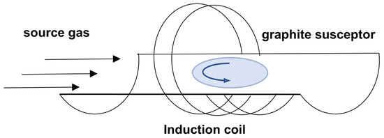
Figure 9.
Schematic diagram of the growth apparatus.
Figure 10 elucidates the mechanism behind the formation of double positioning boundary (DPB) defects during the epitaxial growth process in the 3C-SiC region. As the epitaxy proceeds on the substrate surface, the positions of the interfacial atomic layers between adjacent 3C-SiC and 4H-SiC regions exhibit variability. Notably, 3C-SiC exhibits two distinct stacking domains, namely ABC… and ACB…, and the growth of 3C-SiC selects specific stacking domains based on the initial atomic layer. At the interfaces between these two stacking domains, the occurrence of DPB defects is probable. Furthermore, when different DPB defects intersect, the formation of more pronounced tubular defects becomes possible.
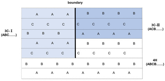
Figure 10.
Schematic diagram of the principle of DPB defect formation. A, B, and C denoted three kinds of stacking positions of SiC crystalline, respectively. The white, the light blue and the dark blue color represent 4H-SiC crystal structure arranged in (ABCB…) stacking sequence, 3C-I crystal structure in (ABC…) sequence and 3C-II in (ACB…) sequence.
4. Conclusions
Using a chemical vapor deposition (CVD) system, we successfully achieved the epitaxial growth of overlapping 3C/4H-SiC on a 4H-SiC substrate (Si-face) with controlled growth rate and source gas concentration. Prior to the growth, we conducted Raman spectroscopy and SEM analyses on different regions of the epitaxial samples. Based on the SEM images, we distinguished the brighter regions as 3C-SiC and the darker regions as 4H-SiC. Notably, in the epitaxial samples grown under moderate source gas flow conditions, a distinct alternation of brightness levels was observed in the cross-sectional SEM images, unequivocally indicating the successful achievement of 3C/4H-SiC stacking epitaxy. Subsequent analysis of cross-sectional views with various orientations revealed a direct correlation between the layered structure and the inclination angle of the substrate. Consequently, we established that the growth of this layered structure was controlled by the micro-nano steps present on the substrate surface. Within this specific structure, multiple 3C/4H heterostructures were observed at the interfaces with the C-face of 4H-SiC. Building upon previous research, these structures were found to possess a high concentration of 2EDG, which underscores their considerable potential for diverse applications.
We conducted an investigation into the impact of varying source gas flow rates on epitaxial SiC growth on a 4H-SiC substrate. The overall trend indicated a progressive deterioration in epitaxial layer quality as the source gas flow rates increased, with a corresponding transition from the 4H crystal phase to the 3C crystal phase. Samples grown under lower source gas flow rates exhibited a congruent crystal structure to the substrate, namely 4H-SiC, and demonstrated superior growth quality, with only minor defects attributed to incidental particle deposition. Conversely, samples grown under higher source gas flow rates displayed a prominent 3C-SiC crystal phase, characterized by a fragmented polycrystalline surface morphology. Notably, this surface exhibited a multitude of DPB defects, accompanied by derived tubular defects and V-shaped trenches. In the case of samples grown under moderate source gas flow rates, the epitaxial surface manifested the simultaneous presence of a central 4H-SiC region and an encircling 3C-SiC region. The central 4H-SiC region revealed discernible step-bunching defects, indicative of relatively diminished growth quality compared to samples grown under lower source gas flow rates. Moreover, the outer ring-shaped region, where 3C-SiC proliferated, exhibited a significantly increased proportion of the platform area compared to the samples grown under higher source gas flow rates, highlighting the heightened quality of epitaxial growth in this context.
Author Contributions
Data curation, methodology, formal analysis, writing—original draft preparation, N.G.; software, visualization, validation, Y.P.; investigation, formal analysis, W.Y.; methodology, S.Y.; software, visualization, S.Z.; supervision, resources, investigation, Y.L.; project administration, investigation, supervision, Y.Z.; conceptualization, supervision, funding acquisition, writing—review and editing, X.L. All authors have read and agreed to the published version of the manuscript.
Funding
This work was supported by the National Key R&D Program of China (Grant No. 2021YFB3401603) and the National Natural Science Foundation of China (Grant No. 12175236).
Data Availability Statement
The data that support the findings of this study are available from the corresponding authors, Y.Z. and X.L., upon reasonable request.
Conflicts of Interest
The authors declare no conflict of interest.
References
- Shi, Y.; Jokubavicius, V.; Höjer, P.; Ivanov, I.G.; Yazdi, G.R.; Yakimova, R.; Syväjärvi, M.; Sun, J. A comparative study of high-quality C-face and Si-face 3C-SiC(1 1 1) grown on off-oriented 4H-SiC substrates. J. Phys. D Appl. Phys. 2019, 52, 345103. [Google Scholar] [CrossRef]
- Liu, G.; Zhang, X.; Yang, J.; Qiao, G. Recent advances in joining of SiC-based materials (monolithic SiC and SiCf/SiC composites): Joining processes, joint strength, and interfacial behavior. J. Adv. Ceram. 2019, 8, 19–38. [Google Scholar] [CrossRef]
- Lebedev, A.A.; Ivanov, P.A.; Levinshtein, M.E.; Mokhov, E.N.; Nagalyuk, S.S.; Anisimov, A.N.; Baranov, P.G. SiC-based electronics (100th anniversary of the Ioffe Institute). Physics-Uspekhi 2019, 62, 754–794. [Google Scholar] [CrossRef]
- La Via, F.; Alquier, D.; Giannazzo, F.; Kimoto, T.; Neudeck, P.; Ou, H.; Roncaglia, A.; Saddow, S.E.; Tudisco, S. Emerging SiC Applications beyond Power Electronic Devices. Micromachines 2023, 14, 1200. [Google Scholar] [CrossRef]
- Matsunami, H. Fundamental research on semiconductor SiC and its applications to power electronics. Proc. Jpn. Acad. Ser. B 2020, 96, 235–254. [Google Scholar] [CrossRef] [PubMed]
- Kimoto, T. Material science and device physics in SiC technology for high-voltage power devices. Jpn. J. Appl. Phys. 2015, 54, 040103. [Google Scholar] [CrossRef]
- Lachichi, A.; Mawby, P. Modeling of Bipolar Degradations in 4H-SiC Power MOSFET Devices by a 3C-SiC Inclusive Layer Consideration in the Drift Region. IEEE Trans. Power Electron. 2022, 37, 2959–2969. [Google Scholar] [CrossRef]
- Jokubavicius, V.; Yazdi, G.R.; Liljedahl, R.; Ivanov, I.G.; Yakimova, R.; Syväjärvi, M. Lateral Enlargement Growth Mechanism of 3C-SiC on Off-Oriented 4H-SiC Substrates. Cryst. Growth Des. 2014, 14, 6514–6520. [Google Scholar] [CrossRef]
- Huczko, A.; Dąbrowska, A.; Savchyn, V.; Popov, A.I.; Karbovnyk, I. Silicon carbide nanowires: Synthesis and cathodoluminescence. Phys. Status Solidi (b) 2009, 246, 2806–2808. [Google Scholar] [CrossRef]
- Chen, J.; Sazawa, H.; Yi, W.; Sekiguchi, T. Cathodoluminescence Study of 3C-SiC Epilayers Grown on 4H-SiC Substrates. J. Electron. Mater. 2023, 52, 5075–5083. [Google Scholar] [CrossRef]
- Narumi, T.; Chaussende, D.; Yoshikawa, T. 3C–, 4H–, and 6H–SiC crystal habitus and interfacial behaviours in high temperature Si-based solvents. CrystEngComm 2020, 22, 3489–3496. [Google Scholar] [CrossRef]
- Chen, X.J.; Li, Y. Stepped morphology on vicinal 3C-and 4H-SiC (0001) faces: A kinetic Monte Carlo study. Surf. Sci. 2019, 681, 18–23. [Google Scholar] [CrossRef]
- Arvanitopoulos, A.E.; Antoniou, M.; Perkins, S.; Jennings, M.; Guadas, M.B.; Gyftakis, K.N.; Lophitis, N. On the Suitability of 3C-Silicon Carbide as an Alternative to 4H-Silicon Carbide for Power Diodes. IEEE Trans. Ind. Appl. 2019, 55, 4080–4090. [Google Scholar] [CrossRef]
- Mukhopadhyay, B.; Basu, P.K.; Basu, R.; Mukhopadhyay, S. Phonon and Alloy Scattering Limited Electron Mobility of Direct Gap Ge1-x Sn-x Alloys. In Proceedings of the 6th International Conference on Computers and Devices for Communication (CODEC), Kolkala, India, 16–18 December 2015. [Google Scholar]
- Sridhara, S.G.; Carlsson, F.H.C.; Bergman, J.P.; Janzén, E. Luminescence from stacking faults in 4H SiC. Appl. Phys. Lett. 2001, 79, 3944–3946. [Google Scholar] [CrossRef]
- Kang, K.-H.; Eun, T.; Jun, M.-C.; Lee, B.-J. Governing factors for the formation of 4H or 6H-SiC polytype during SiC crystal growth: An atomistic computational approach. J. Cryst. Growth 2014, 389, 120–133. [Google Scholar] [CrossRef]
- Agati, M.; Boninelli, S.; Calabretta, C.; Mancarella, F.; Mauceri, M.; Crippa, D.; Albani, M.; Bergamaschini, R.; Miglio, L.; La Via, F. Growth of thick [111]-oriented 3C-SiC films on T-shaped Si micropillars. Mater. Des. 2021, 208, 109833. [Google Scholar] [CrossRef]
- Sun, Q.Y.; Yang, M.J.; Li, J.; Xu, Q.F.; Tu, R.; Li, Q.Z.; Zhang, S.; Zhang, L.M.; Goto, T.; Ohmori, H.; et al. Heteroepitaxial growth of thick 3C-SiC (110) films by Laser CVD. J. Am. Ceram. Soc. 2019, 102, 4480–4491. [Google Scholar] [CrossRef]
- Abou Hamad, V.; Soueidan, M.; Hamad, H.; Gremillard, L.; Fabregue, D.; Zgheib, C.; Zaatar, Y. Thermo-Mechanical Simulation of Self-Heating of a High-Power Diode Made of Ti3SiC2 (MAX) Phase-on-4H-SiC Substrate. J. Therm. Sci. 2021, 30, 939–949. [Google Scholar] [CrossRef]
- Sultan, N.M.; Albarody, T.M.B.; Al-Jothery, H.K.M.; Abdullah, M.A.; Mohammed, H.G.; Obodo, K.O. Thermal Expansion of 3C-SiC Obtained from In-Situ X-ray Diffraction at High Temperature and First-Principal Calculations. Materials 2022, 15, 6229. [Google Scholar] [CrossRef]
- Zhang, X.; Liu, X.S.; Wang, Y.Z.; Zhu, R.Z.; Zhang, X.Q.; Zhang, Y.Q.; Wang, R.; Yang, D.R.; Pi, X.D. Optimizing the flatness of 4H-silicon carbide wafers by tuning the sequence of lapping. Semicond. Sci. Technol. 2023, 38, 034001. [Google Scholar] [CrossRef]
- Feng, Z.C.; Lin, H.H.; Xin, B.; Tsai, S.J.; Saravade, V.; Yiin, J.; Klein, B.; Ferguson, I.T. Structural characteristics of 3C-SiC thin films grown on Si-face and C-face 4H-SiC substrates by high temperature chemical vapor deposition. Vacuum 2023, 207, 111643. [Google Scholar] [CrossRef]
- Li, X.; Jacobson, H.; Boulle, A.; Chaussende, D.; Henry, A. Double-Position-Boundaries Free 3C-SiC Epitaxial Layers Grown on On-Axis 4H-SiC. ECS J. Solid State Sci. Technol. 2014, 3, P75. [Google Scholar] [CrossRef]
- Xin, B.; Jia, R.X.; Hu, J.C.; Tsai, C.Y.; Lin, H.H.; Zhang, Y.M. A step-by-step experiment of 3C-SiC hetero-epitaxial growth on 4H-SiC by CVD. Appl. Surf. Sci. 2015, 357, 985–993. [Google Scholar] [CrossRef]
- Wu, J.; Qian, S.T.; Huo, T.G.; Zheng, J.X.; Zhang, P.L.; Dai, Y.; Geng, D.S. Effect of PyC Inner Coating on Preparation of 3C-SiC Coating on Quartz Glass by Chemical Vapor Reaction. Front. Mater. 2022, 9, 897900. [Google Scholar] [CrossRef]
- Kawanishi, S.; Daikoku, H.; Shibata, H.; Yoshikawa, T. Suppressing solvent compositional change during solution growth of SiC using SiC/C gradient crucible. J. Cryst. Growth 2021, 576, 126382. [Google Scholar] [CrossRef]
- Sannodo, N.; Osumi, A.; Kaminaga, K.; Maruyama, S.; Matsumoto, Y. Vapour-liquid-solid-like growth of high-quality and uniform 3C-SiC heteroepitaxial films on alpha-Al2O3(0001) substrates. Crystengcomm 2021, 23, 1709–1717. [Google Scholar] [CrossRef]
- Schuh, P.; Scholer, M.; Wilhelm, M.; Syvajarvi, M.; Litrico, G.; La Via, F.; Mauceri, M.; Wellmann, P.J. Sublimation growth of bulk 3C-SiC using 3C-SiC-on-Si (100) seeding layers. J. Cryst. Growth 2017, 478, 159–162. [Google Scholar] [CrossRef]
- Xin, B.; Jia, R.X.; Hu, J.C.; Zhang, Y.M. Super-V-shaped structure on 3C-SiC grown on the C-face of 4H-SiC. J. Phys. D-Appl. Phys. 2016, 49, 335305. [Google Scholar] [CrossRef]
- Qin, X.; Li, X.; Chen, X.; Yang, X.; Zhang, F.; Xu, X.; Hu, X.; Peng, Y.; Yu, P. Raman scattering study on phonon anisotropic properties of SiC. J. Alloys Compd. 2019, 776, 1048–1055. [Google Scholar] [CrossRef]
- Sazawa, H.; Yamaguchi, H. High-mobility 2D electron gas in carbon-face 3C-SiC/4H-SiC heterostructure with single-domain 3C-SiC layer. Appl. Phys. Lett. 2022, 120, 212102. [Google Scholar] [CrossRef]
- Burton, W.K.; Cabrera, N.; Frank, F.C. The growth of crystals and the equilibrium structure of their surfaces. Philos. Trans. R. Soc. Lond. Ser. A Math. Phys. Sci. 1951, 243, 299–358. [Google Scholar] [CrossRef]


Disclaimer/Publisher’s Note: The statements, opinions and data contained in all publications are solely those of the individual author(s) and contributor(s) and not of MDPI and/or the editor(s). MDPI and/or the editor(s) disclaim responsibility for any injury to people or property resulting from any ideas, methods, instructions or products referred to in the content. |
© 2023 by the authors. Licensee MDPI, Basel, Switzerland. This article is an open access article distributed under the terms and conditions of the Creative Commons Attribution (CC BY) license (https://creativecommons.org/licenses/by/4.0/).