Article

Influence of Growth Time and Temperature on Optical Characteristics and Surface Wetting in Nano-Crystalline Graphene Deposited by PECVD Directly on Silicon Dioxide

by
Algimantas Lukša
1,*,
Virginijus Bukauskas
1,
Viktorija Nargelienė
1,
Marius Treideris
1,
Martynas Talaikis
2,
Algirdas Selskis
3,
Artūras Suchodolskis
4 and
Arūnas Šetkus
1
1
Department of Physical Technologies, State Research Institute Center for Physical Sciences and Technology (FTMC), Saulėtekio Av. 3, LT-10257 Vilnius, Lithuania
2
Department of Organic Chemistry, State Research Institute Center for Physical Sciences and Technology (FTMC), Saulėtekio Av. 3, LT-10257 Vilnius, Lithuania
3
Department of Structural Analysis of Materials, State Research Institute Center for Physical Sciences and Technology (FTMC), Saulėtekio Av. 3, LT-10257 Vilnius, Lithuania
4
Department of Optoelectronic, State Research Institute Center for Physical Sciences and Technology (FTMC), Saulėtekio Av. 3, LT-10257 Vilnius, Lithuania
*
Author to whom correspondence should be addressed.
Crystals 2023, 13(8), 1243; https://doi.org/10.3390/cryst13081243
Submission received: 20 July 2023 / Revised: 3 August 2023 / Accepted: 9 August 2023 / Published: 11 August 2023
(This article belongs to the Special Issue Research on Nonlinear Optics with 2D Materials)

Abstract

:
Unique electronic properties of graphene offer highly interesting ways to manipulate the functional properties of surfaces and develop novel structures which are sensitive to physical and chemical interactions. Nano-crystalline graphene is frequently preferable to crystalline monolayer in detecting devices. In this work, nano-crystalline graphene layers were synthesized directly on SiO2/Si substrates by plasma-enhanced chemical vapour deposition (PECVD). The influence of the deposition time and temperature on the characteristics of the structures were studied. The optical properties and evaporation kinetics of pure water droplets were analysed, along with arrangement and composition of the grown layers. The nano-crystalline graphene layers grown at 500 °C were characterised by the refraction index 2.75 ± 0.35 and the normalised excess Gibbs free energy density 0.85/γwater 10−4 m, both being similar to those of the monolayer graphene. The changes in the refraction index and the excess Gibbs free energy were related to the parameters of the Raman spectra and a correlation with the technological variables were disclosed.

1. Introduction

Direct growth of graphene layers on substrates seems a highly attractive approach in the technology of electronic and photonic devices. Promising ways to combine optical and electrical properties were demonstrated by mixing two-dimensional (2D) and three-dimensional (3D) graphene structures produced by an adapted chemical vapour deposition (CVD) on the same substrate [1]. On the one hand, the CVD process temperatures are typically too high (about 800 °C) for technology of combined electronic devices, but, on the other hand, the technology studies were useful and some basic graphene structures were demonstrated on insulating substrates, combining direct CVD with sacrificial catalytic layers [2]. Development of plasma-enhanced chemical vapour deposition (PECVD) for direct graphene growth on solid surfaces has recently been suggested as a promising way to reduce the process temperature without catalyst layers [3,4]. The method was successful tested for direct deposition of graphene structures on dielectric and semiconducting substrates [5], insulating SiO2 [6], Si(100) [7], Ge(100) and Ge(110) [8]. In spite of the success, some doubts were pointed out regarding reduction in the process temperature and complexity of the technique [9]. However, the advantages of PECVD are still highly attractive because of the variety of radicals, molecules and ions that are produced during PECVD process. These aspects of the technology offer interesting ways to develop one-step, large and small-scale production of devices with low-cost synthesis of graphene layers and graphene-based functional films on diverse substrates [10]. Flexibility in modification of properties of the structures can be additionally increased by adapting the growth of specific vertically aligned nanosheets [11]. Although the PECVD process depend on the technical characteristics of the plasma [4,5,7,10], the substrate temperature [6,9,12] and growth time [12,13] are the most practical variables to change the properties of the films in the early stages when the influence of the substrate cannot be ignored. It was demonstrated recently [12] that the structure of the films can be specifically controlled by a combination of the temperature and the growth time in a low-temperature (<650 °C) PECVD process. Therefore, it is highly important to understand the influence of this combination on the properties of graphene-based structures produced by PECVD technology.
Previous studies proved [13] that very thin graphene-based films (several monolayers or less) are arranged as sheets parallel to the surface of the substrate. Even in such thin films, an influence of the graphene layers on the properties of the supporting structure was reliably detected in visible spectra of the optical reflection [13,14]. Adapting a SiO2/Si-based Fabry–Perot resonator in the experiments, the optical reflection spectra showed that the refractive index and extinction coefficient are unique to each of the few-layer structures [15]. The numerical values are dependent on the thickness, up to the bulk limit of graphite [16]. The graphene-related changes in the optical properties were demonstrated for various structures on diverse substrates [17]. However, it is quite easy to notice significant differences between the parameters in separate studies [17,18], even if specific constraints were used in the experiments, such as in [18]. Though the sample preparation technology seems quite reasonable as an explanation of the scattering between results, assumptions about graphene–substrate interaction-dependent changes suggested an interesting possibility to develop specific graphene-based structures for physical and chemical detectors. However, more detailed understanding about the relationships between the technology conditions and the characteristics of the structures are required.
Interaction between water and graphene is highly sensitive to the diverse properties of 2D graphene structures, depending on the studied phenomena and the dominant mechanisms. Wetting transparency of substrate-supported graphene was interpreted in terms of the surface–graphene van der Waals interaction and specific binding states related to the arrangement of the structure on rough surfaces [19,20]. Comprehensive analysis of the wetting studies revealed new avenues to manipulate the wetting of the surfaces by graphene structure engineering based on fundamental understanding of the dominant mechanisms [21]. The model descriptions of effects frequently introduced the surface free energy and work of adhesion as a quantitative property that can be extracted from experiments [21,22]. For this, corresponding wetting contact angle was used for quantitative characterization of the interaction energy [23]. Theoretical models were proposed to relate the work of adhesion obtained from measurements with the features of the molecule–surface interaction [24] and microscopic parameters such as the site binding energy [25]. The understanding of the graphene wetting features is frequently enhanced by more sophisticated methods of investigation. Recently, optical and electrical methods were successfully combined in a specific spectroscopy of the interface water that was in contact with CVD graphene surfaces [26]. The findings about the complexity of the water–graphene interaction suggested a possibility to use the water on graphene system for analysis of a relationship between the direct deposition technology conditions and the properties of the graphene-based structures. For this, it is important to reveal a correlation between optical properties, wetting parameters and the morphological features of the substrate-supported graphene.
In this work, nano-crystalline graphene was experimentally characterized by optical reflection spectra and evaporation kinetics of pure water droplets. The graphene samples were prepared by plasma-enhanced chemical vapour deposition (PECVD) on silicon substrates with insulating silicon dioxide film (SiO2/Si). The arrangement and composition of the layers were related with the parameters obtained from the model description of the optical spectra and the evaporation kinetics. Possibilities to simultaneously modify the optical and wetting properties by choices in the technological conditions were analysed. A correlation between the characteristic parameters of both types of properties was analysed, aiming to simplify comparison of the graphene layers grown under diverse technological conditions. The analysis was mainly focused on the parameters which are important in development of the plasmonic based detecting devices.

2. Materials and Methods

2.1. Film Deposition Method

Nano-crystalline films were deposited using plasma-enhanced chemical vapour deposition technology. For this, a PECVD furnace from SVCS (SVCS Process Innovation s.r.o, Brno, Czech Republic) was used. A more detailed deposition method was presented in a previous work [12]. The samples were deposited at six different temperatures: 400 °C, 450 °C, 500 °C, 550 °C, 600 °C and 650 °C. Temperature in the deposition zone was ensured by three heaters. Deposition time was between 0.5 and 3 h, depending on the sample. Argon (5 N purity) with added hydrogen of 5% by volume was used as the transport gas. Methane (5.5 N) gas was used as a carbon precursor. Precursor and transport gas flow rates during deposition were 5 sccm and 900 sccm, respectively. Plasma was ignited on this stage and was set to 775 W. Gas pressure in the chamber was 1 Torr (133 Pa). Before and after the deposition stage, the flow rate was 300 sccm of pure transport gas.
Samples were placed downstream from the plasma source by about 3.5 cm. Electronic-grade silicon, coated with 250 (±5%) nm SiO2 film (SIEGERT WAFER Gmbh, Aachen, Germany) as a substrate, was used.

2.2. Surface Characterization

Surface morphology was studied by atomic force microscopy (AFM) and scanning electron microscopy (SEM). An AFM Dimension 3100/Nanoscope-IVa (Veeco, New York, NY, USA) was used in the tapping mode for the characterisation of the samples. FEI Helios Nanolab 650 (FEI, Eindhoven, The Netherlands) was used for scanning electron microscopy imaging of the samples.

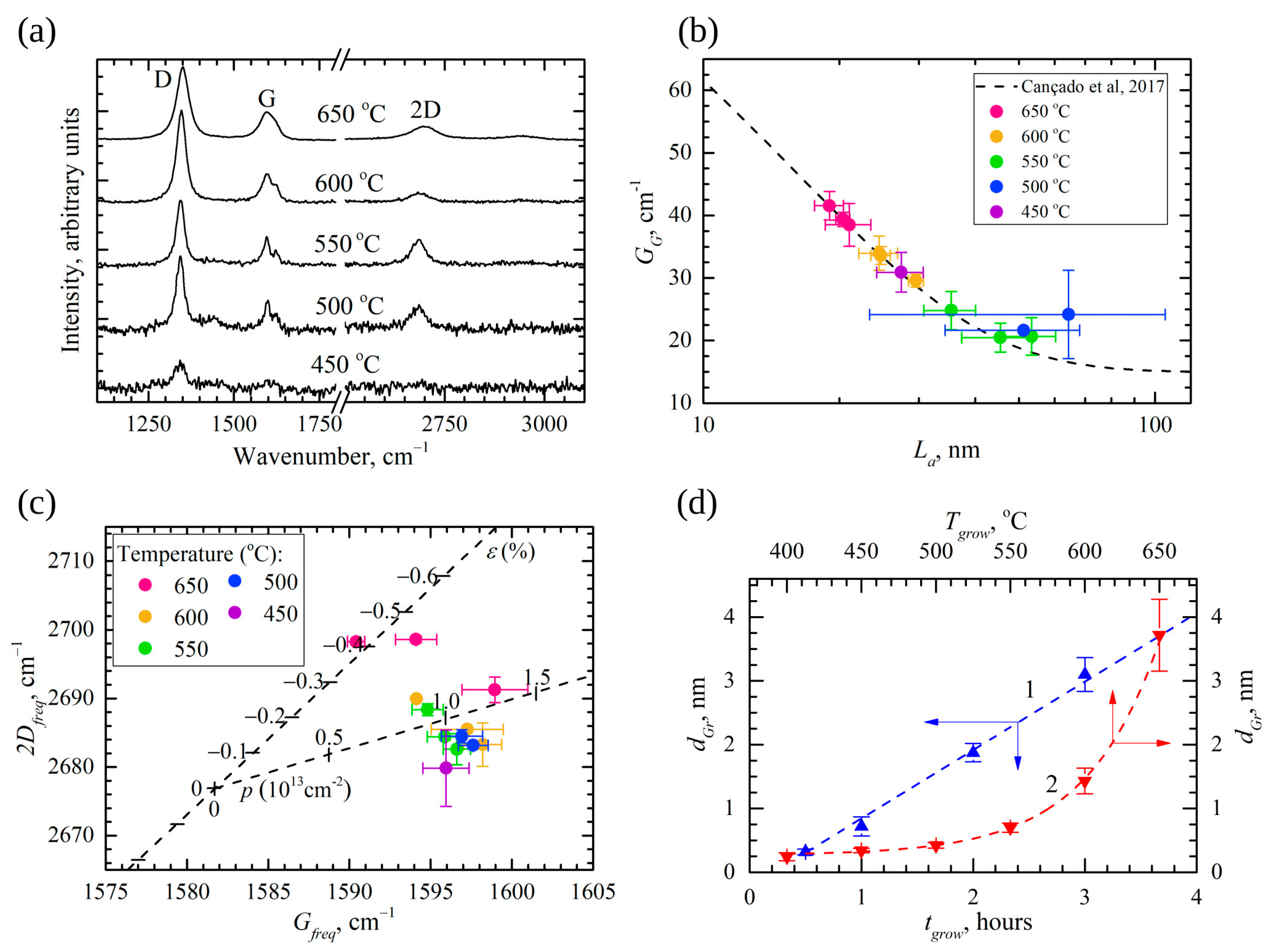
2.3. Raman Spectroscopy

Raman spectrometer InVia (Renishaw, Gloucestershire, UK) was used to measure Raman spectra of the samples. Laser radiation of 0.45 mW power at 532 nm was used for Raman scattering excitation. Raman spectra were collected from the spot of 1 μm diameter using a 50×/0.75 (NA) objective lens (Leica Microsystems, Wetzlar, Germany), dispersed on 1800 grooves/mm grating and registered with a thermoelectrically cooled (−70 °C) CCD camera. The Lorentzian function was used to fit measured Raman spectrum peaks of nano-crystalline graphene samples.

2.4. Optical Measurements

A UV-3600 (Shimadzu, Kyoto, Japan) two-beam spectrometer, equipped with a multi-purpose compartment MPC-3100 containing an integrating sphere of 60 mm diameter coated with barium sulphate, was used for cumulative measurements of diffusive and specular reflectance spectra. The incident angle of 8 degrees was used in specular reflectance measurement. All spectra were obtained relative to a barium sulphate target.

2.5. Contact Angle Tests

Water droplet evaporation experiments were performed using an optical contact angle measuring system KSC CAM101 (KSV Instruments Ltd., Helsinki, Finland). A droplet of water was lowered on the surface of the substrate and recorded by a CCD camera. Recording continued until the droplet became invisible, with measurements taken every 30 s. The same volume of droplets was used in all measurements and was equal to 2.3 μL.

3. Results

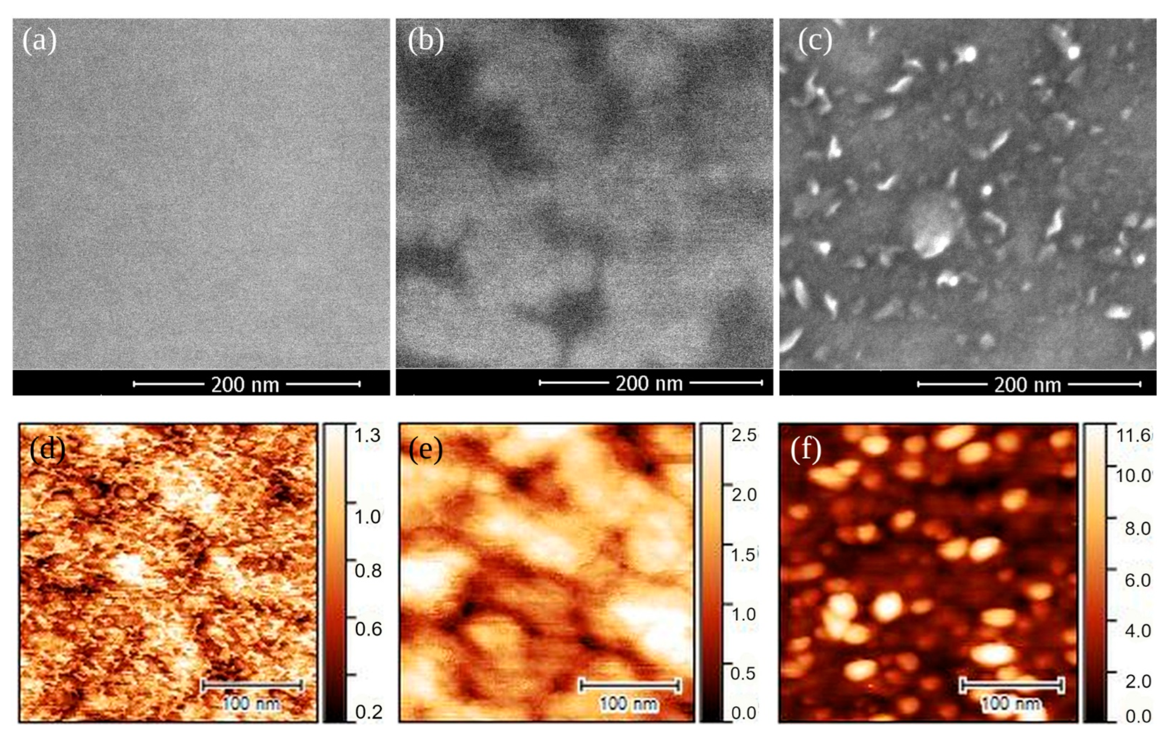
3.1. Arrangement and Composition

The surface morphology of the nano-crystalline graphene layers was visualised by SEM and AFM topography images, as shown in Figure 1. The images illustrate the most typical arrangement of the surfaces of the layers grown at temperatures equal to 450 °C, 550 °C and 650 °C.
Based on the surface arrangement, three intervals of the growth temperatures were identified as resulting in three types of morphology during the direct PECVD deposition on the insulating SiO2. The classification of the layers was based on recent AFM results presented in [12]. The lower temperature morphology type was comparably smooth layers obtained by deposition at Tgrow ≤ 450 °C. At middle temperatures, flat clusters, about 50–100 nm diameter, were tightly packed in a practically continuous layer grown at 450 °C ≤ Tgrw ≤ 600 °C. It must be noted here that the height variation was within an interval from about 0.5 nm to 2.5 nm and could be mostly associated with the areas between the clusters in these layers. The high-temperature morphology layers included protruding columns that were easily identified above the flat clusters in the SEM and AFM images in the layers grown at Tgrw ≥ 650 °C. More detailed analysis of the arrangement of the surfaces of the layers were reported in work [12].
Analysis of the Raman spectra suggested a large amount of defects in the nano-crystalline graphene layers. Typical Raman spectra were illustrated in Figure 2a. The spectra were measured for the layers grown at individual Tgrow. The experimental results proved that the Raman 2D and G modes were detected in the spectra of the SiO2-supported graphene layers. However, the intensity of the Raman D mode was clearly higher for all the studied layers. This fact suggested the presence of a large amount of the defects. Therefore, the spectra were analysed in more detail.
The full width at half maximum (FWHM) ΓG for the G mode of the Raman spectra was numerically described according to the method from the literature [27]. The dimensions of the nano-crystalline graphene flakes were calculated using ΓG. It followed from these calculations that the size of the nano-crystals was up to about 50 nm. These obtained dimensions were in good agreement with the dimensions of the flat cluster size measured by the AFM surface scan. The Raman spectra analysis are graphically presented by the dependences of ΓG versus the flake dimensions in Figure 2b. In the figure, the results of our study are plotted with the background of summarised information from the literature [27]. A detailed analysis of the Raman spectra, including the ratios of the main peaks that characterise the graphene and the AFM topography of the grown layers, has been reported in a recent paper [12], whereas, here, only the findings of this analysis are included. It can be noted here that a part of the defects can be associated with the grain boundaries limiting the area of the flat surfaces of the graphene clusters (see [12]). Such arrangement of the surfaces was used to explain the stick–slip motion of the three-phase contact line during the droplet evaporation, described below in this text.
An influence of the interaction between the layer and the substrate was quantitatively characterised by correlation between the position of 2D and G Raman modes. It has been shown that the correlation between the frequencies of the G and 2D Raman modes of graphene plots can be used to separate mechanical strain and charge doping effects in graphene layers [28]. Following this methodology, the frequency of 2D mode 2Dfreq versus frequency of G mode Gfreq of nano-crystalline graphene is plotted in Figure 2c. Dashed lines in Figure 2c are the slopes of mechanical strain and charge doping dependences [28]. As followed from this correlation, the layers were quantitatively described by the strain ε ≈ 0, whereas the p-doping density of the layers was on the order of (1–1.5) × 1013 cm−2. Though the scattering of the points representing separate samples was noticeable in the graphs in Figure 2c, only the layers grown at 650 °C during separate processes were more distinct from each other than expected.
The thickness of the layers was obtained from the AFM scans performed on the samples with the strips of bare SiO2 surfaces. The heights of the step-like edge were obtained for all the samples and are summarised in Figure 2d. In addition, more detailed analysis of the thicknesses of the layers can be found in [12]. In the figure, typical dependences of the thickness on the technological parameters are graphically shown. The figure illustrates only the results of two series of the samples, namely, thickness dGr vs. growth time tgrow and thickness dGr vs. growth temperature Tgrow, with the film thicknesses including the thickest layers in this test. In the case dGr vs. tgrow, the temperature was constant and equal to 650 °C, whereas the layers were grown during the same time equal to 3.0 h at individual constant temperatures. It followed from these results that the minimal thickness was about 0.3 nm. The thickness increased linearly with the growth time, whereas the increase in the growth temperature resulted in an exponential increase in the thickness of the nano-crystalline graphene. In all cases, the maximum thickness of the studied layers was less than about 3.8 nm, though a significant scattering within about ±0.6 nm was obtained for these thick layers. The increase in the uncertainty of the thickness measurements was explained by specific arrangement of the layers containing clearly protruding columns above the comparably smooth basic surfaces. It must be noted here that the thicknesses in dgrow vs. Tgrow in Figure 2d were specifically re-defined by including the modified thicknesses obtained from the fitting of the reflection spectra. An adjustment was implemented in the AFM-measured thickness to minimize disparities between the calculated and experimental reflection spectra. Since these corrections were not applied in dgrow vs. tgrow, it can be seen (in Figure 2d) that these modifications were, practically, within the accuracy limits. However, taking into account that the reflection was obtained from the spot with a diameter of about 1 mm, these results also suggested an idea that a variation in the layer thickness was slightly larger over entire sample than within the AFM-tested step area, i.e., 100 × 100 μm2.

3.2. Optical Reflectance

An influence of the growth time and temperature on the properties of the SiO2-supported nano-crystalline graphene layer was analysed based on the optical reflection spectra measured for all the studied samples in the interval of wavelengths between 250 nm and 700 nm. Typical experimental spectra are presented for the layers with different growth time tgrow and temperature Tgrow in Figure 3a and Figure 3b, respectively. Interference caused a decrease in the intensity of the minima at about 300 nm and 500 nm. The decrease in the intensity was quantitatively described by a model of two films stacked together (nano-crystalline graphene and SiO2) between a silicon substrate and the surrounding air. The model calculations were limited to the single minimum because fitting of the model with the experiment can be simplified by neglecting the parameter dependence on wavelength. In addition, thin-film approximation, which neglects the phase retardation associated with transmission through and reflection from graphene, was also used to simplify the model description [15]. Typical results of the model fitting with the experiment are illustrated in Figure 3c. The calculated refractive index at 500 nm nGr (500) are graphically presented as the dependences on growth temperature and duration in Figure 3d.
The dependences nGr at 500 nm vs. tgrow and nGr at 500 nm vs. Tgrow in Figure 3d disclose a specific influence of the growth temperature on the index. This effect cannot be related with the changes in the thickness of the layers. An increase in the thickness along with increase in growth time of the nano-crystalline graphene layer resulted in a low but noticeable decrease in the refractive index nGr(500) from about 2.0 to about 1.75 in the interval of the thicknesses dGr < 1.4 nm. However, an influence of the temperature Tgrow on nGr(500) was highly specific in these very thin layers. An increase from about 2.2 to about 2.7 was detected for nGr(500) when the growth temperature was increased from 400 °C to 500 °C. The index decreased down to about 1.7 in the layers grown at higher temperatures Tgrow > 550 °C. An increase in the thickness of the layers with the growth temperature can be explained by an increase in the growth rate, as was reported in detail in [12] and, thus, was not analysed in this work. However, the changes in the thickness can hardly be related to the unexpected nGr(500) increase at Tgrow = 500 °C because the changes in the thickness were in an extremely narrow interval 0.3 ≤ dGr ≤ 0.7 nm for these samples and the effects of both tgrow and Tgrow on nGr(500) were similar on the edges and outside the interval of these thicknesses. The observed variations in the refractive index may be attributed to the structural changes caused by different growth temperatures.

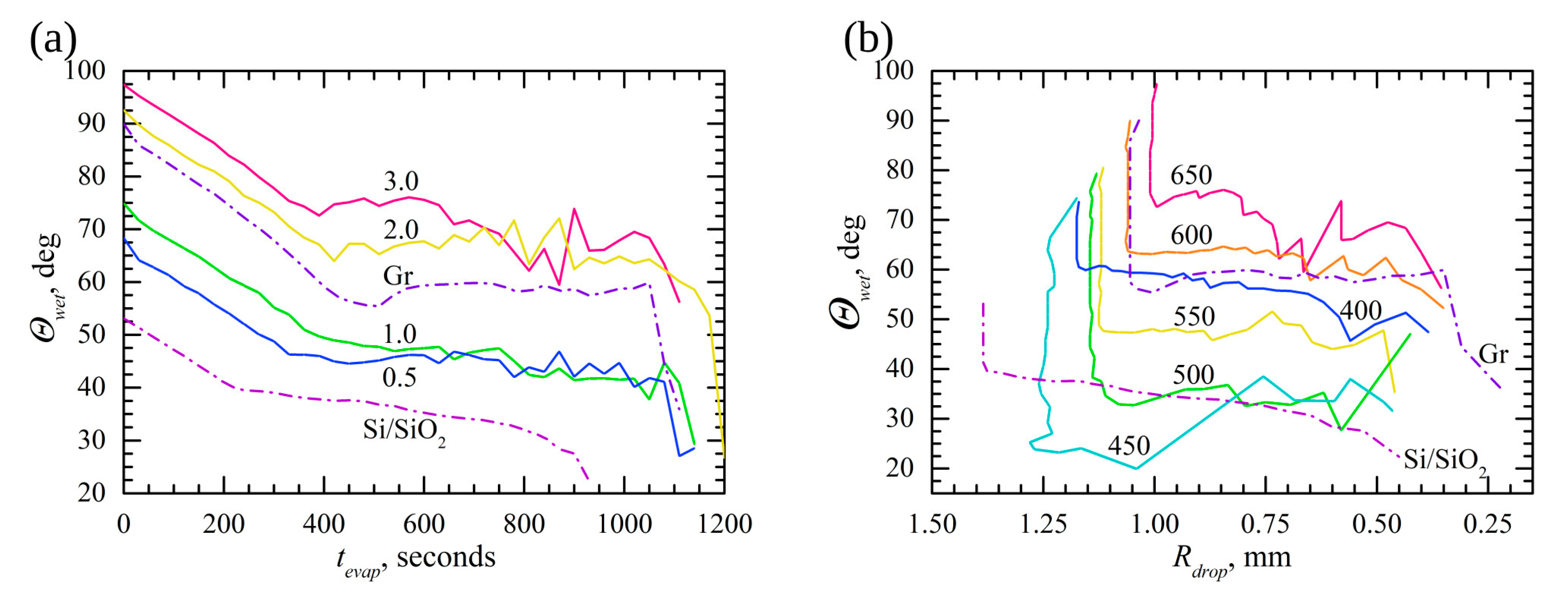
3.3. Droplet Evaporation Dynamics
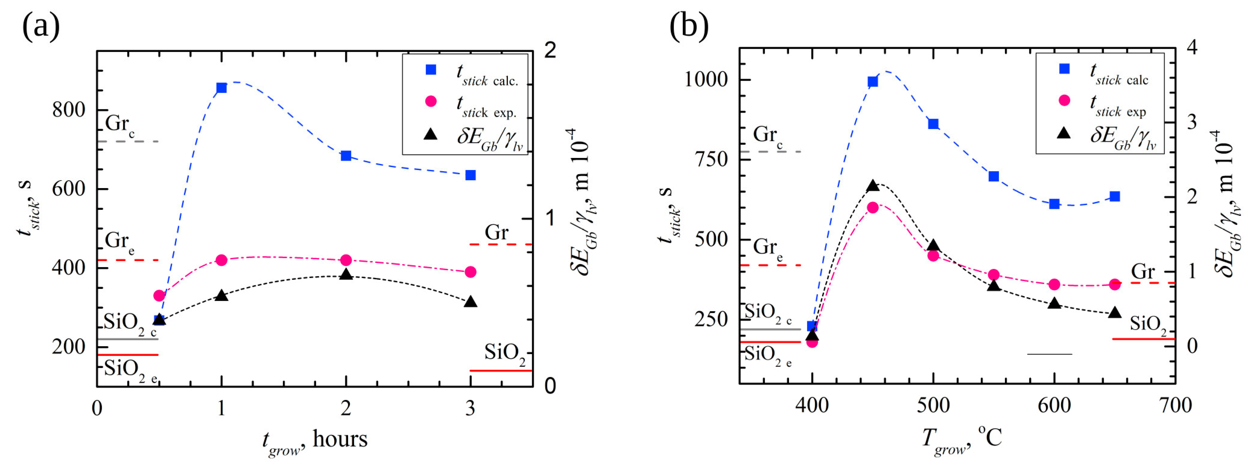
The properties of the surfaces were compared with each other in the series of SiO2-supported nano-crystalline graphene layers using individual sets of specific parameters obtained from the experiments with water droplet evaporation. The experimental results of the water droplet evaporation tests are illustrated in Figure 4.
Typical dependence of the wetting angle Θwet on evaporation time is graphically plotted in Figure 4a. The dependences were obtained for the series of the nano-crystalline graphene layers grown on SiO2/Si substrate at 650 °C for individual growth time in hours tgrow = 0.5, 1.0, 2.0 and 3.0. For comparison, in Figure 4a similar dependences were also illustrated for the bare SiO2/Si substrate and a clean commercial graphene monolayer on a SiO2/Si substrate. The dependences of Θwet on water evaporation time tevap were also measured for the nano-crystalline layers grown at different temperatures. Aiming to demonstrate visually specific stages in evaporation kinetics, the results Θwet versus tevap are graphically presented as dependences of Θwet versus droplet radius Rdrop in Figure 4b. For comparison, the same characteristics of the droplet evaporation were measured for both the bare surface of the SiO2/Si substrate and a clean commercial monolayer graphene sheet on a SiO2/Si substrate. In the kinetics of the droplet evaporation, two typical evaporation stages, namely, Constant Contact Angle (CCA) and Constant Contact Radius (CCR), were reliably detected. The angle Θwet linearly decreases in the CCR stage at the beginning of evaporation tevap < 400 s (Figure 4a), though the duration of the CCR stage was clearly different for each of the layers with unique thickness. The CCA stage can be visually identified between about 400 and 900 s in Figure 4a. The duration of this stage was clearly dependent on the layer thickness. The stages CCA and CCR were much more visually prominent in the dependences present in the specific form in Figure 4b. Vertical lines visualise the CCR stage, whereas the horizontal lines depict the CCA stage for the layers grown at individual substrate temperature Tgrow. Several specific aspects were identified in the characteristics of the droplets on the surfaces. First, the initial wetting angle Θwet0(tevap = 0) increased from about 68° to about 98° with an increase in the thickness of the nano-crystalline graphene layer dGr from about 0.3 nm (tgrow = 0.5 h) to about 3.4 nm (tgrow = 3.0 h). Second, the dependence of the initial angle versus layer deposition temperature Tgrow was non-monotonous and reached a minimum for the layers grown at Tgrow = 500 °C. Third, sufficiently evident sharp variations were detected for the wetting angle in the CCA stage on most of the nano-crystalline layers. These sharp variations reliably indicated the stick–slip nature in the droplet volume reduction during the evaporation.
The parameters of the droplet evaporation kinetics were clearly different from those of the bare SiO2 surfaces. For example, Θwet0 and duration of the CCR stage were evidently larger for the nano-crystalline graphene layers than that for the bare SiO2. In contrast to this, the monolayer graphene was characterized by the evaporation parameters similar to one or two groups of the nano-crystalline graphene. For example, the monolayer was comparable with the layers grown for 2.0 h at 650 °C and with those grown for 3.0 h at 550 °C and 600 °C. Overall, the parameters of the droplet evaporation kinetics were highly sensitive to the growth duration and substrate temperature and were acceptable as the criteria for classification of the layers, as well as for comparison with the bare SiO2 surfaces and the SiO2-supported monolayer graphene sheet.

4. Discussion

It is quite easy to understand an influence of the growth duration on the measured properties of the nano-crystalline graphene layers. The thickness of the layers linearly increased with the PECVD growth duration. Screening of the substrate properties and formation of a three-dimensional arrangement can be accepted as two dominant effects which result in changes in the properties of SiO2-supported nano-crystalline graphene. The substrate screening effect was directly suggested by a decrease in the intensity of the Si Raman mode at about 520 cm−1 in the Raman spectra. These results were thoroughly discussed in [12]. The substrate screening effect could also be the primary origin of the increase in the initial contact angle in the water droplet evaporation experiments illustrated in Figure 4a. However, this increase was comparable with that measured for the reference samples with the commercial monolayer of graphene. Considering commonly accepted wetting transparency of monolayer graphene for SiO2 [19], the substrate screening effect can hardly explain the droplet evaporation dynamics for the samples with comparatively thin nano-crystalline graphene coating. On the other hand, the wetting transparency can hardly be accepted for the layers thicker than about 2 nm corresponding to ≥5 monolayers. It can be expected that the nano-crystalline graphene would much more similar to a three-dimensional structure if the thickness exceeded 5–10 monolayers of graphene.
Aiming to separate between influences of growth conditions and substrate on properties of nano-crystalline graphene, an evaporation model was adapted from the literature for calculations of interaction energy on the surfaces. Several approaches can be found for the model description in literature [20,23,28]. The models include the fundamental Young’s equation for a liquid droplet on solid surfaces:
γ s v γ s l = γ l v c o s Θ w 0
where γsv, γsl, γlv are the tensions in the solid-state, solid–liquid and liquid–vapour interfaces. The contact angle Θw0 describes the wetting of the solid surfaces at the equilibrium. The Gibbs free energy of the interface EGb can be described as
E G b = S C γ s l γ s v + S A γ l v
where SC and SA are areas of the solid–liquid and liquid–vapour contact surfaces. An interaction between solid and vapour is commonly neglected compared to the solid–liquid interface. Disk-like area SC and spherical cap area SA can easily be related with the droplet contact radius RD for a droplet with spherical symmetry. The excess Gibbs free energy δEGb = Egb(RD) − EGb(RD0) is then equal to
δ E G b = γ l v 2 π R 2 Θ w 0 Θ w 2 2 2 + c o s Θ w 0
Analogous to [29], the normalized energy δEGb/γlv per unit length of the three-phase contact line was calculated and is graphically presented in Figure 5. It must be noted here that RD0 and Θw0 were measured at equilibrium after a droplet landed on the surface, whereas RD and Θw were obtained at the end of the CCA stage. Calculated energy δEGb versus growth time tgrow and growth temperature Tgrow are depicted in Figure 5a and Figure 5b, respectively. The sticking time tstick is also presented graphically in Figure 5 as the layer-specific parameter which is acceptable to detect the changes in the adhesion forces produced by the changes in the layer growth conditions.
The sticking time tstick was obtained according to the algorithm in [29]. Two numerical values were calculated for the sticking time in each evaporation test. The duration of the CCA (until the first jump of the three-phase contact line) was the directly measured sticking time tstick, whereas the calculated one was obtained from the formula derived on the basis of the evaporation rate t*stick, as presented in [29]. Both these values are plotted on the graphs in Figure 5 as dependences on growth time tgrow and temperature Tgrow. As the reference criteria, the stick times and excess Gibbs free energy of the bare SiO2 surface and the graphene monolayer are denoted by horizontal lines in Figure 5.
Both the excess Gibbs free energy δEGb and the sticking time tstick of the SiO2 substrate were almost the same as for nano-crystalline graphene layers (dGr ≤ 0.36 nm) grown at 400 °C. Parameters δEGb and tstick were much closer to those of the commercial graphene monolayer than the SiO2 surface for nano-crystalline layer grown at higher temperatures. Considering the relationship between microscopic parameters, including the molecular binding energy and macroscopic wetting properties in [25], the surface bonds on the insulating SiO2 surfaces were completely screened by the nano-crystalline graphene grown at Tgrow ≥ 450 °C because δEGb of these layers was significantly higher than that of the substrate. When δEGb and tstick of nano-crystalline graphene and graphene monolayer were compared, a similarity was identified to layers grown at 500 °C and 550 °C. Combining this fact with the increase in the refraction index up to about 2.7 for these layers in Figure 3d, it was accepted that the nano-crystalline layers grown at temperatures 500 °C ≤ Tgrow ≤ 550 °C were practically analogous to the graphene monolayer with respect to the optical and the surface interaction properties.
It was also interesting to note that the experimental sticking time tstick and the time t*stick calculated according to the formula in [29] were significantly different one from another for almost all the layers, except for that grown at Tgrow = 400 °C. The results in Figure 5b illustrate that the sticking time (both calculated and measured) displayed nearly the same correlation with the growth temperature and duration as the excess Gibbs free energy. The calculated sticking time represented an evaporation-related droplet shrinking model based on sticking of the droplet boundary due to the water–surface interaction that determined the excess Gibbs free energy for the modified SiO2 surfaces. Compared to the calculated one, the shorter experimental sticking time can be explained by a polarization of local charge clusters in the nano-crystalline layers, as was suggested in [29]. Due to the omission of the polarization effect in the calculations, the observed difference revealed the change in the surface–droplet interaction mechanism. The differences were negligible only for the layers grown at Tgrow = 400 °C for 3 h. This can be explained by the very low dimensions of the flakes and the high amount of defects in the atomically thin graphene layer. The idea was also supported by the same differences in Figure 5a in the extremely thin layers grown at 650 °C for 0.5 h. The screening of the SiO2 polarisation effect in droplet shrinking occurred if the deposited layers were composed of the detectable flakes of graphene and a few layers of the graphene. In these samples, the features of the substrate surface were completely screened in the droplet evaporation process. Since the same effects were detected for the samples with the commercial graphene monolayers, it was suggested that the easy measurable sticking time can be highly useful in controlling the graphene deposition process, especially because there was quite close correlation between the changes in the parameters of the surface wetting and the optical characteristics.

5. Conclusions

In summary, it can be accepted that this study demonstrated sufficiently interesting flexibility in possibilities to modify the optical and wetting properties of the nano-crystalline layers by changing the process temperature and duration in the PECVD technology. It follows from this study that a combination of two technological parameters, namely, the growth time and the growth temperature, are a quite effective combination of technological variables when aiming to tune the functional properties of nano-crystalline graphene. The changes in the refraction index proved that the optical properties of the nano-crystalline graphene can be close to that of a monocrystalline graphene if the PECVD process is performed at substrate temperatures 500 °C ≤ Tgrow ≤ 550 °C. Moreover, the wetting characteristics of these layers can also be changed to make them close to that of a graphene monolayer. These nano-crystalline graphene layers completely screened the features of the underlaying SiO2 film. In contrast to this, the nano-crystalline graphene layers directly grown on the SiO2 surfaces at about 400 °C were completely transparent to the binding features of the SiO2 surfaces. Based on the results of this study, the parameters of the droplet evaporation dynamics can be accepted as highly useful criteria for control of the layer properties.

Author Contributions

Conceptualization, A.L., V.N. and A.Š.; formal analysis, A.Š.; investigation, A.L., V.B., A.S. (Algirdas Selskis) and A.S. (Artūras Suchodolskis); resources, V.B., M.T. (Marius Treideris), M.T. (Martynas Talaikis), A.S. (Algirdas Selskis) and A.S. (Artūras Suchodolskis); writing—original draft preparation, A.Š.; writing—review and editing, A.Š., A.L., M.T. (Marius Treideris) and V.N.; visualization, A.Š., A.L. and V.N.; supervision, A.Š.; project administration, A.Š.; funding acquisition, A.Š. All authors have read and agreed to the published version of the manuscript.

Funding

This research received no external funding.

Data Availability Statement

The data presented in this study are available on request from the corresponding author.

Conflicts of Interest

The authors declare no conflict of interest.

References

  1. Marchena, M.; Song, Z.; Senaratne, W.; Li, C.; Liu, X.; Baker, D.; Ferrer, J.C.; Mazumder, P.; Soni, K.; Lee, R.; et al. Direct Growth of 2D and 3D Graphene Nano-Structures over Large Glass Substrates by Tuning a Sacrificial Culate Layer. 2D Mater. 2017, 4, 025088. [Google Scholar] [CrossRef] [Green Version]
  2. Dong, Y.; Guo, S.; Mao, H.; Xu, C.; Xie, Y.; Deng, J.; Wang, L.; Du, Z.; Xiong, F.; Sun, J. In Situ Growth of CVD Graphene Directly on Dielectric Surface toward Application. ACS Appl. Electron. Mater. 2020, 2, 238–246. [Google Scholar] [CrossRef]
  3. Li, M.; Liu, D.; Wei, D.; Song, X.; Wei, D.; Wee, A.T.S. Controllable Synthesis of Graphene by Plasma-Enhanced Chemical Vapor Deposition and Its Related Applications. Adv. Sci. 2016, 3, 1600003. [Google Scholar] [CrossRef]
  4. Yi, K.; Liu, D.; Chen, X.; Yang, J.; Wei, D.; Liu, Y.; Wei, D. Plasma-Enhanced Chemical Vapor Deposition of Two-Dimensional Materials for Applications. Acc. Chem. Res. 2021, 54, 1011–1022. [Google Scholar] [CrossRef] [PubMed]
  5. Khan, A.; Islam, S.M.; Ahmed, S.; Kumar, R.R.; Habib, M.R.; Huang, K.; Hu, M.; Yu, X.; Yang, D. Direct CVD Growth of Graphene on Technologically Important Dielectric and Semiconducting Substrates. Adv. Sci. 2018, 5, 1800050. [Google Scholar] [CrossRef] [Green Version]
  6. Muñoz, R.; Martínez, L.; López-Elvira, E.; Munuera, C.; Huttel, Y.; García-Hernández, M. Direct Synthesis of Graphene on Silicon Oxide by Low Temperature Plasma Enhanced Chemical Vapor Deposition. Nanoscale 2018, 10, 12779–12787. [Google Scholar] [CrossRef]
  7. Meškinis; Vasiliauskas, A.; Guobienė, A.; Talaikis, M.; Niaura, G.; Gudaitis, R. The Direct Growth of Planar and Vertical Graphene on Si(100) via Microwave Plasma Chemical Vapor Deposition: Synthesis Conditions Effects. RSC Adv. 2022, 12, 18759–18772. [Google Scholar] [CrossRef]
  8. Bekdüz, B.; Kaya, U.; Langer, M.; Mertin, W.; Bacher, G. Direct Growth of Graphene on Ge(100) and Ge(110) via Thermal and Plasma Enhanced CVD. Sci. Rep. 2020, 10, 12938. [Google Scholar] [CrossRef]
  9. Li, C.; Zheng, C.; Cao, F.; Zhang, Y.; Xia, X. The Development Trend of Graphene Derivatives. J. Electron. Mater. 2022, 51, 4107–4114. [Google Scholar] [CrossRef]
  10. Yeh, N.C.; Hsu, C.C.; Bagley, J.; Tseng, W.S. Single-Step Growth of Graphene and Graphene-Based Nanostructures by Plasma-Enhanced Chemical Vapor Deposition. Nanotechnology 2019, 30, 162001. [Google Scholar] [CrossRef] [Green Version]
  11. Zhou, F.; Shan, J.; Cui, L.; Qi, Y.; Hu, J.; Zhang, Y.; Liu, Z. Direct Plasma-Enhanced-Chemical-Vapor-Deposition Syntheses of Vertically Oriented Graphene Films on Functional Insulating Substrates for Wide-Range Applications. Adv. Funct. Mater. 2022, 32, 2202026. [Google Scholar] [CrossRef]
  12. Lukša, A.; Nargelienė, V.; Treideris, M.; Bukauskas, V.; Talaikis, M.; Šetkus, A. Stages of Self-Arrangement in Growth of Nanostructured Graphene Films Related to the Flow of Ionized Species during Plasma-Enhanced Chemical Vapor Deposition. J. Vac. Sci. Technol. A 2023, 41, 53402. [Google Scholar] [CrossRef]
  13. Shin, K.W.; Cho, Y.; Lee, Y.; Lee, H.; Nam, S.G.; Byun, K.E.; Lee, C.S.; Park, S.; Shin, H.J. Study of Selective Graphene Growth on Non-Catalytic Hetero-Substrates. 2D Mater. 2020, 7, 011002. [Google Scholar] [CrossRef]
  14. Gray, A.; Balooch, M.; Allegret, S.; De Gendt, S.; Wang, W.E. Optical Detection and Characterization of Graphene by Broadband Spectrophotometry. J. Appl. Phys. 2008, 104, 053109. [Google Scholar] [CrossRef]
  15. Ghamsari, B.G.; Tosado, J.; Yamamoto, M.; Fuhrer, M.S.; Anlage, S.M. Measuring the Complex Optical Conductivity of Graphene by Fabry-Pérot Reflectance Spectroscopy. Sci. Rep. 2016, 6, 34166. [Google Scholar] [CrossRef] [Green Version]
  16. Bruna, M.; Borini, S. Optical Constants of Graphene Layers in the Visible Range. Appl. Phys. Lett. 2009, 94, 031901. [Google Scholar] [CrossRef]
  17. Barrutia, L.; Ochoa-Martínez, E.; Gabás, M.; Centeno, A.; Zurutuza, A.; Rey-Stolle, I.; Algora, C. Evidence of Decreased Optical Absorption of Chemical Vapor Deposition Graphene Multilayers Deposited on Semiconductor Structures. ACS Photonics 2022, 9, 868–872. [Google Scholar] [CrossRef]
  18. Cheon, S.; Kihm, K.D.; Kim, H.G.; Lim, G.; Park, J.S.; Lee, J.S. How to Reliably Determine the Complex Refractive Index (RI) of Graphene by Using Two Independent Measurement Constraints. Sci. Rep. 2014, 4, 6364. [Google Scholar] [CrossRef] [Green Version]
  19. Li, W.; Cheng, G.; Liang, Y.; Tian, B.; Liang, X.; Peng, L.; Hight Walker, A.R.; Gundlach, D.J.; Nguyen, N.V. Broadband Optical Properties of Graphene by Spectroscopic Ellipsometry. Carbon 2016, 99, 348–353. [Google Scholar] [CrossRef] [Green Version]
  20. Kim, D.; Pugno, N.M.; Buehler, M.J.; Ryu, S. Solving the Controversy on the Wetting Transparency of Graphene. Sci. Rep. 2015, 5, 15526. [Google Scholar] [CrossRef] [Green Version]
  21. Parobek, D.; Liu, H. Wettability of Graphene. 2D Mater. 2015, 2, 032001. [Google Scholar] [CrossRef]
  22. Wang, S.; Zhang, Y.; Abidi, N.; Cabrales, L. Wettability and Surface Free Energy of Graphene Films. Langmuir 2009, 25, 11078–11081. [Google Scholar] [CrossRef] [PubMed]
  23. Leroy, F.; Liu, S.; Zhang, J. Parametrizing Nonbonded Interactions from Wetting Experiments via the Work of Adhesion: Example of Water on Graphene Surfaces. J. Phys. Chem. C 2015, 119, 28470–28481. [Google Scholar] [CrossRef]
  24. Taherian, F.; Marcon, V.; Van Der Vegt, N.F.A.; Leroy, F. What Is the Contact Angle of Water on Graphene? Langmuir 2013, 29, 1457–1465. [Google Scholar] [CrossRef] [PubMed]
  25. Ramos-Alvarado, B. Water Wettability of Graphene and Graphite, Optimization of Solid-Liquid Interaction Force Fields, and Insights from Mean-Field Modeling. J. Chem. Phys. 2019, 151, 114701. [Google Scholar] [CrossRef]
  26. Dreier, L.B.; Liu, Z.; Narita, A.; Van Zadel, M.J.; Müllen, K.; Tielrooij, K.J.; Backus, E.H.G.; Bonn, M. Surface-Specific Spectroscopy of Water at a Potentiostatically Controlled Supported Graphene Monolayer. J. Phys. Chem. C 2019, 123, 24031–24038. [Google Scholar] [CrossRef] [Green Version]
  27. Cançado, L.G.; Da Silva, M.G.; Martins Ferreira, E.H.; Hof, F.; Kampioti, K.; Huang, K.; Pénicaud, A.; Achete, C.A.; Capaz, R.B.; Jorio, A. Disentangling Contributions of Point and Line Defects in the Raman Spectra of Graphene-Related Materials. 2D Mater. 2017, 4, 025039. [Google Scholar] [CrossRef]
  28. Lee, J.E.; Ahn, G.; Shim, J.; Lee, Y.S.; Ryu, S. Optical Separation of Mechanical Strain from Charge Doping in Graphene. Nat. Commun. 2012, 3, 1024. [Google Scholar] [CrossRef] [Green Version]
  29. Bormashenko, E.; Musin, A.; Zinigrad, M. Evaporation of Droplets on Strongly and Weakly Pinning Surfaces and Dynamics of the Triple Line. Colloids Surfaces A Physicochem. Eng. Asp. 2011, 385, 235–240. [Google Scholar] [CrossRef]
Figure 1. Topography images produced by SEM (ac) and AFM (df) for the nano-crystalline graphene layers grown by the PECVD for 3.0 h on SiO2/Si substrates at Tgrow = 450 °C (a,d), 550 °C (b,e) and 650 °C (c,f). Height is in nm in AFM colour scale.
Crystals 13 01243 g001
Figure 2. (a) Raman spectra of the nano-crystalline graphene grown at temperatures 450 °C, 500 °C, 550 °C, 600 °C and 650 °C for 3.0 h. (b) Relationship between the full width at half maximum of the Raman G mode ΓG and the flake diameter La: lines represent calculations according to [27], points are the experiments of the current work. (c) Relationship between the strain ε (%) and doping density p (1013 cm−2), represented within graphically plotted correlations between the Raman modes 2D and G. (d) Dependences of the layer thickness dGr on growth time tgrow (blue colour, samples grown at 650 °C) and growth temperature Tgrow (red colour, samples grown for 3.0 h): points are experimental, lines are an approximation.
Crystals 13 01243 g002
Figure 3. Optical reflection spectra and corresponding refraction index for the nano-crystalline graphene layers on insulating SiO2 surfaces: (a) grown at 650 °C for individual time (in hours): 0.5; 1.0; 2.0; 3.0; (b) grown for 3.0 h at individual growth temperature: 400 °C; 450 °C; 500 °C; 550 °C; 600 °C; 650 °C. (c) Extrema of the optical reflection spectra from (b) at 500 nm: model calculations (lines) fitted with the experiment (points) for the nano-crystalline graphene grown at 400 °C; 550 °C; 600 °C and 650 °C for 3.0 h. (d) Dependences of the refractive index nGr at wavelength 500 nm for graphene layers versus thickness of the layer dGr (blue colour—grown at 650 °C at different durations; red colour with empty triangles—grown at different temperatures for 3.0 h) and growth temperature Tgrow (red colour with solid circles): points are experimental, lines are eye-guides.
Crystals 13 01243 g003
Figure 4. (a) Dependences of wetting angle Θwet on water droplet evaporation time tevap for the nano-crystalline graphene layers grown at 650 °C for individual tgrow (hours): 0.5; 1.0; 2.0; 3.0. (b) Dependences of Θwet on droplet radius Rdrop for nano-crystalline graphene grown for 3.0 h at Tgrow: 400 °C; 450 °C; 500 °C; 550 °C; 600 °C; 650 °C. For comparison: SiO2 is the bare substrate and Gr is a commercial graphene monolayer.
Crystals 13 01243 g004
Figure 5. Correlation between model parameters and technological variables, namely, growth time tgrow and temperature Tgrow: (a) sticking time tstick and normalized excess Gibbs free energy δEGb/γlv versus tgrow; (b) tstick and δEGb/γlv versus Tgrow for the layers of the nano-crystalline graphene. Dashed lines provide guides to the eye.
Crystals 13 01243 g005
Disclaimer/Publisher’s Note: The statements, opinions and data contained in all publications are solely those of the individual author(s) and contributor(s) and not of MDPI and/or the editor(s). MDPI and/or the editor(s) disclaim responsibility for any injury to people or property resulting from any ideas, methods, instructions or products referred to in the content.

