Article

Annihilation and Generation of Dislocations by Irradiation by Ions and Electrons in Strontium Titanate Single Crystal

1
Institute of Physics—Center for Science and Education, Silesian University of Technology, Krasińskiego 8 Street, 40-019 Katowice, Poland
2
Institute of Energy and Climate Research (IEK-14), Forschungszentrum Jülich GmbH, 52425 Jülich, Germany
3
Marian Smoluchowski Institute of Physics, Faculty of Physics, Astronomy and Applied Computer Science, Jagiellonian University, Lojasiewicza 11, 30-348 Krakow, Poland
4
International Centre of Electron Microscopy for Materials Science, Faculty of Metals Engineering and Industrial Computer Science, AGH University of Science and Technology, 30-059 Krakow, Poland
5
A. Chełkowski Institute of Physics, University of Silesia, 41-500 Chorzów, Poland
6
aixACCT Systems GmbH, 52068 Aachen, Germany
*
Author to whom correspondence should be addressed.
Crystals 2023, 13(8), 1259; https://doi.org/10.3390/cryst13081259
Submission received: 4 July 2023 / Revised: 12 August 2023 / Accepted: 13 August 2023 / Published: 15 August 2023
(This article belongs to the Section Inorganic Crystalline Materials)

Abstract

:
The physical and chemical properties of many oxide materials depend strongly on their defect concentration, which gives rise to unique electronic, optical, and dielectric properties. One such promising material for various applications, including energy storage, photocatalysis, and electronics, is SrTiO3 (STO). It exhibits several interesting phenomena, including a metal-to-insulator transition that can be induced by reduction. By extension, 1-D defects, such as dislocations, play a significant role in its electronic properties. Thus, we investigate the process of dislocation movement, its creation, and annihilation under two stimuli: ion thinning and electron irradiation. First, we designed and produced a lamella from a mechanically modified sample with variable thickness in the form of a wedge using a focused ion beam (FIB/Ga+) to investigate thickness-dependent dislocation movement. The lamella was investigated by transmission electron microscopy, allowing for the measurements of dislocation concentration as a function of its thickness. We have noticed a sharp decrease in the defect concentration with respect to the starting sample, showing a process of annihilation of dislocations. Second, we used an electron beam to drive a relatively large current into the STO surface. This experiment produced an electrical breakdown-like pattern. Optical and atomic force microscopy revealed that this pattern evolved due to the removal of material from the surface and local metal-insulator-transition along the dislocations network. Thus, we observe the dislocations generation and movement.

1. Introduction

The strontium titanate perovskite (SrTiO3—STO) is considered a model material thanks to its simple cubic crystal structure and availability of high-quality crystals [1]. It exhibits many unique electronic, optical, and dielectric properties [2]. STO holds many applications in energy storage [3], photocatalysis [4], and electronics [5,6]. While stoichiometric STO is an insulator, it can be transformed into an n-type semiconductor and even into a metal by introducing oxygen vacancies through a redox process. Many of these exciting properties originate from the defects found in the STO. Extended defects, such as dislocations in particular, play a tremendous role in the STO crystals. They introduce dangling bonds, lower the bandgap, change local chemistry, can serve as easy diffusion paths for O and Sr ions, and play a crucial role in the insulator-to-metal transition induced by either thermal reduction or electro-degradation [7]. Research on low-angle tilt grain boundaries of STO bicrystals recently provided new opportunities to observe dislocations in a more controller manner. The core of Ti-rich dislocations in STO was shown to consist of TinO2n−1 phases, with n close to 1, supporting the evolution of Magnéli-type conducting filaments along a dislocation upon reduction [8]. Other recent results also found that the dislocation core exhibits flexoelectric polarization induced by a strain gradient [9]. This polarization induces a bound charge, which has to be screened by a free carriers redistribution or defect accumulation, which also influences the electrical behavior of the whole STO structure. A further study shows even the possibility of inducing ferroelectric-(anti)ferromagnetic-multiferroic phase transition [10]. Such transitions are confined to only a few unit cells around the dislocation core. Nevertheless, since they are embedded in the ambient paraelectric host, it is theorized that they can act as nanometer-sized ferroelectric-(anti)ferromagnetic-multiferroic channels, similar to a concept of electrical ones [11].
Hence, even though dislocations have traditionally been avoided in classical semiconductors due to their detrimental effects on carrier mobility and functional properties, they are proven to provide enhanced functionalities in oxides. Using mechanical stress and plastic deformation, one can increase the number of dislocations or move the existing ones [12,13]. This, in turn, can be controllable to enhance desired properties, such as electrical conductivity [14]. However, using other methods to generate or annihilate dislocations would be beneficial. Thus, in this article, we investigate two methods: ion thinning (decrease of the dislocation concentration through size effect) and electron irradiation (increase concentration and movement of dislocations).

2. Materials and Methods

The samples consist of undoped SrTiO3 single crystals manufactured by the Verneuil method from high-purity powders. They were obtained commercially from the Crystec company (Berlin, Germany). Typical starting sample dimensions were 10 mm × 10 mm × 1 mm with a (100) polished surface.
The samples used for the cross-sectional investigation (the lamella formation) were first mechanically modified (scratched) and etched with HF/NH4F solution for 30 s. Mechanical scratching (roughening using a diamond tip) is known to introduce extended defects, mainly dislocations and bundles of dislocations [15]. The concentration of the defect at the surface reaches 1012/cm2 [12]. The surface of the STO was then investigated by scanning electron microscopy (SEM) to identify the etched pyramids, marking the exits of dislocations [16]. Next, a small region with a relatively high density of dislocations was chosen for the ex-situ lift-out technique. This region, with approximate dimensions of 7 μm × 7 μm × 1 μm, was covered with platinum and cut from the crystal by the FIB. Further, the sample was transferred into another holder where its sides were thinned, as shown in Figure 1a,b, with different gallium ion energies starting from 30 keV, then 5 keV, and finally 2 keV. This kind of FIB preparation procedure produces a high-quality STO thin sample suitable for atomically resolved HAADF STEM, as we showed previously [17]. The produced lamella was shaped like a wedge with three different thicknesses: smallest in the middle and thickest on the sides, as shown in Figure 1c. The final thicknesses of the wedge are 58 nm to 79 nm, 108 nm to 206 nm, and 162 nm to 343 nm from the sample surface region toward the STO bulk. For simplicity, we will reference them in the text as 58 nm, 108 nm, and 162 nm.
The sample cross-section was imaged with a scanning transmission electron microscope (STEM) operated at 300 keV in the High Angle Annular Dark Field (HAADF) mode shown in Figure 2a. The STEM-HAADF measurements confirmed the atomic structure of STO (see Figure 2b). The signal intensity is proportional to the square of the atomic number and sample thickness.
For the electron irradiation experiments, pristine STO crystals were used. The 1 mm thick SrTiO3 (100) samples were glued to the copper base with a silver paste. An electron-beam vacuum welder was used source for electron irradiation. The acceleration voltage was set to 30 keV, and a current of 50 μA irradiated the surface for a duration of 50 μs. Thus, a total charge of 2.5 nC was applied to the spot 0.5 mm in diameter, resulting in the current density of 2.55 × 10⁶ A/cm2.

3. Results and Discussion

Two different methods to modify the STO defect structure were used:
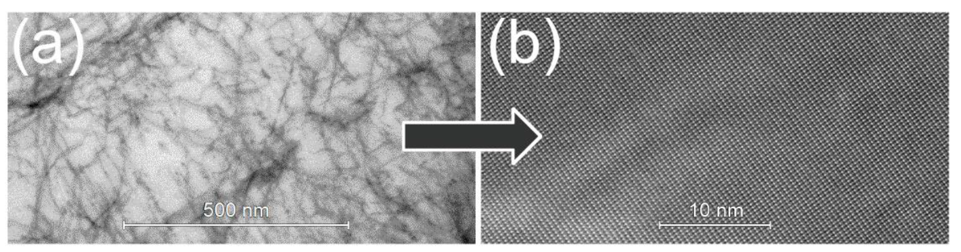
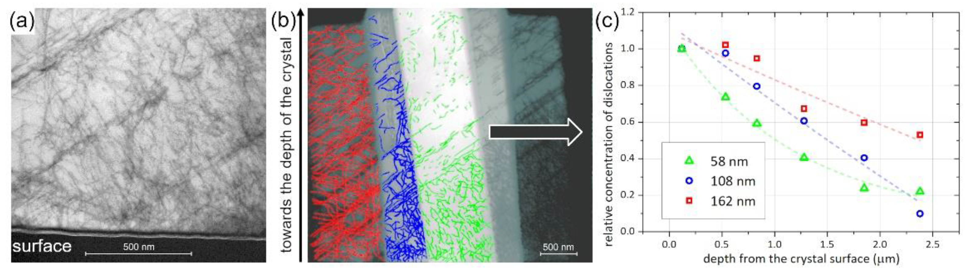
  • The first approach focused on ion bombardment during lamella preparation and its influence on the dislocation concentration. The STEM observation allowed us to directly observe defect structure along the (110) direction and measure a dislocation concentration as a function of the sample thickness and depth from the crystal surface. It allowed us to observe the annihilation of dislocations in the surface region of the STO crystal.
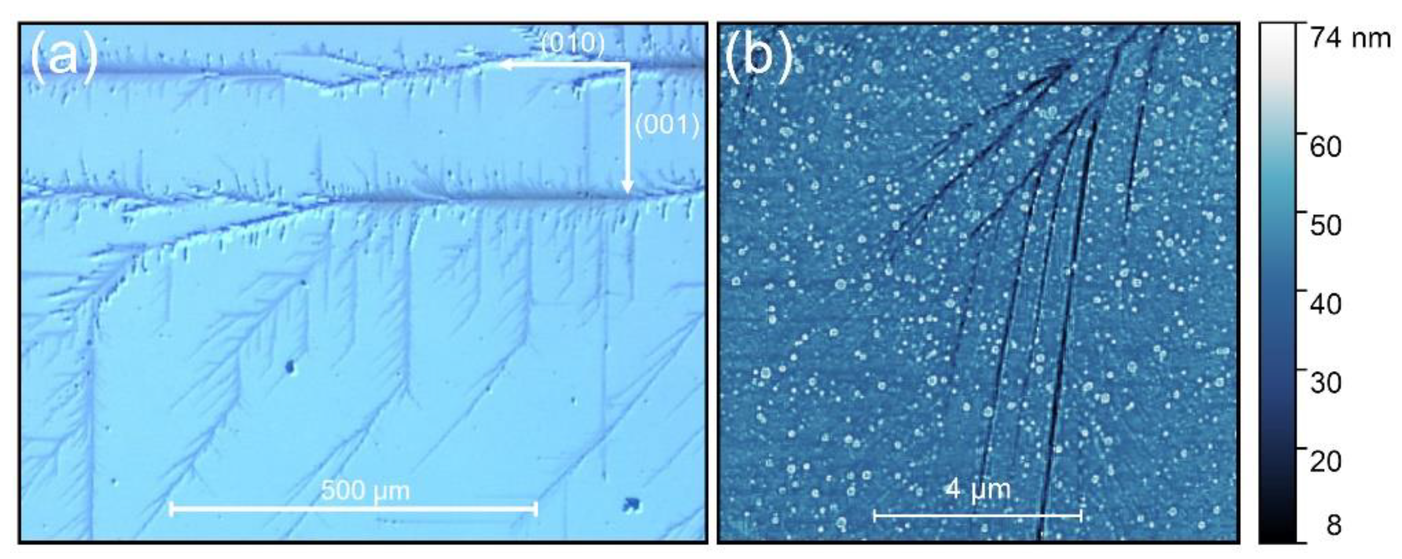
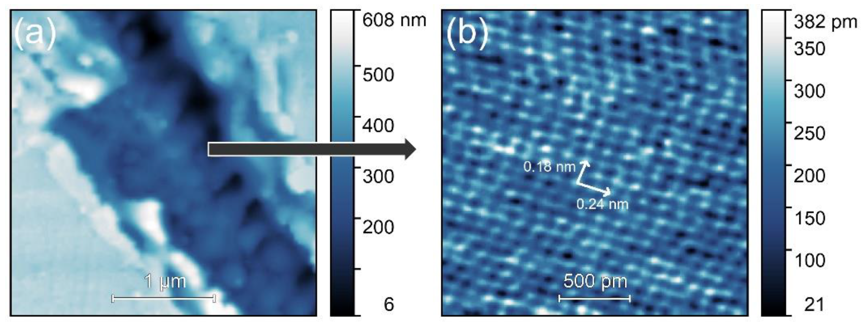
  • The second approach implemented electron irradiation from a high-voltage source. It led to the formation of visible patterns along (010), (001), and (011) directions, which are typical for electro-degradation and resistive switching on the STO crystal surface. Such patterns mirror the arrangement of the extended defects found in the crystal, which can be investigated by optical and atomic force microscopy. It allowed us, in turn, to observe the generation and movement of dislocations in the measured sample.

3.1. Decrease of Dislocation Density in an STO Lamella Induced by Thinning with the Focused Ion Beam

We have investigated how the thinning performed by the FIB modifies the dislocation density on initially uniformly produced STO lamella. The obtained sample was perfectly suitable for atomically resolved HAADF STEM, as shown in Figure 3a.
In order to measure the dislocation density, the HAADF STEM image of the lamella with different thicknesses was analyzed, as seen in Figure 3b. The total length of the observed dislocations was measured in three different parts of the wedge-type lamella corresponding to different sample thicknesses. Those thicknesses were 58 nm (green), 108 nm (blue), and 162 nm (red). By dividing the STEM-HAADF image into separate regions in the form of rhombic-like cells, we have obtained the dislocation concentrations from the surface to 2.5 μm toward the crystal bulk. Knowing the region’s geometry (volume), we were able to calculate the dislocation concentration versus the depth from the crystal surface, as summarized in Figure 3c (The wedge lamella thickness changes effects are included).
One has to keep in mind that the starting surface layer of STO crystal exhibits a relatively high number of dislocations—typically in the range of 109–1010/cm2 for epi-polished surfaces. In our case, the dislocation density on the surface was even higher, around 1012/cm2, due to mechanical modification (scratching [18]). We discovered that the average dislocation concentration on the lamella surface was equal to 2.1 × 10¹⁰/cm2. This is already two orders of magnitude lower than the initial concentration. At a depth of 2.5 μm, the dislocation concentration is further lower by approximately one order of magnitude. Thus are starting to be similar to those for the as-received crystal in the low 109/cm2 range [19]. For all investigated thicknesses, the general trend is very similar—the concentration of defects is highest for the smaller distance to the surface, which is consistent with our previous investigations and existing literature [12,20]. However, the evolution of concentration with the distance to the crystal surface is much different for different thicknesses of the STO lamella. Thus, the thinner the part, the faster the concentration drops, which reveals a size-dependent annihilation of dislocations at the surface. Dislocations can annihilate by moving (gliding or climbing) to the free surface [19]. As a result, an additional step will be formed on the surface due to the shifting of the structure by half-plane. The ion bombardment process can enhance that effect by producing an electric field or causing mechanical stress at the surface. Such higher fields can interact more effectively with the stress field of the dislocations or their ferro- or flexoelectric polarization [9] and thus cause faster gliding or climbing of these extended defects towards the surface and, in the final stage, lead to their annihilation on the surface.
We also have to mention that various literature data [21,22,23] show that ion bombardment can also increase the defect concentration due to ion implantation, mechanical stress (ion damage), or temperature gradients. However, we analyzed those effects in detail and concluded that the increase in the defect concentration due to ion bombardment is negligible:
  • Ion implantation—The calculations of the penetration range of Ga ions into the STO matrix were done by the SRIM/TRIM software [24]. The calculations for the grazing angle and 2 keV (final step of the thinning) beam gave a 2.5 Å penetration range, roughly half of the unit cell of the STO. This effect would be much more prominent in the FIB milling technique, where Ga accumulation can cause the formation of new phases [25]. However, this is not the case, and due to the short penetration depth, we can assume that the ion implantation will not influence the defect concentration much.
  • Ion damage—the thinning process was done under a grazing angle, but still, the ions carry significant mass and energy, which can modify the sample surface deep into the bulk. In principle, the damage done by the FIB is proportional to the range of Ga ion implantation [26]. For a similar case (in terms of energy) of Si crystal, a 2 keV Ga beam used for polishing is able to cause amorphization of 0.5–1.5 nm surface [27]. In our case, the penetration range was equal to 2.5 Å. However, a non-stoichiometric STO is especially susceptible to ion damage [21]. Thus, one can expect that the ion beam caused enough damage to form an amorphous layer of at most a few nm.
  • Temperature gradients—the evaluation of the exact temperature gradient is rather difficult, as it depends on the FIB parameters, sample properties (thermal conductivity), and geometry. The available data do not show a significant global temperature change, especially during lamella formation. Some data on limiting FIB damage to soft matter like tissues show significant temperature changes of 250 °C [28]. However, the modeling was done on a material with a significantly worse thermal conductivity coefficient than STO (by a factor of 8). Since the temperature increase is strongly dependent on this parameter, we can estimate that the temperature increase has to be much smaller than in the presented example.
What is more, we do not see an increase in the defect concentration from the experiment.

3.2. Increase of Dislocation Density and Its Role in Electrical Pattern Formation Caused by Electron Irradiation from a High-Voltage Source

In order to investigate the effect of high-density electron irradiation, we studied the STO crystal under exposure to a high-voltage electron beam. We have irradiated the STO surface with a large density current (2.55 × 10⁶ A/cm2). Within 50 ns, the patterns of tree-like features, similar to Lichtenberg Figures [29], emerged, as seen in Figure 4 by optical and atomic force microscopy. The AFM topography measurement revealed that the elongated craters are of a depth ranging from 20 nm up to several 350 nm for the biggest ones (Figure 4b). Thus, the feature is formed on the surface due to the removal of STO material. The observed figures differ significantly from the results of electro-reduction at low electric fields and elevated temperatures, which did not reveal a significant removal of STO material [18,30].
What is most important is that the observed patterns are not randomly oriented but follow the main crystallographic directions of (001), (010), and (011) instead. Moreover, even though the bottom of the crystal was grounded, we did not observe any filaments penetrating the bulk, revealing that it is a surface effect. This is related to the fact that the surface region has the highest dislocation density compared to deeper regions. It is known that the bulk dislocation concentration in STO depends on the growth techniques employed and is only equal to 105 and 107/cm2 for Czochralski and Verneuil techniques, respectively [18]. However, due to the existing dislocation network, the current travels more easily through the crystal edges.
What is also significant is the mechanism of this (Lichtenberg) pattern formation. One has to remember that an as-received STO crystal is an insulator with a relatively large band gap of 3.2 eV. However, it can undergo electro-degradation and metal-insulator transition by oxygen vacancy formation. Each oxygen vacancy introduces two electrons into the conduction band under a sufficiently high electric field [18]. The electric field will drive negatively charged oxygen ions toward the positive potential (a virtual anode), where they could leave the crystal as oxygen molecules. If the incorporation of oxygen from the surrounding atmosphere is significantly smaller than the excorporation at the anode (which is the case in ambient conditions), a process of electro-reduction occurs. Such a process is very local since the oxygen vacancy formation enthalpy at dislocations is significantly smaller than in bulk [31]. Thus, a vacancy-rich filament with a high charge carrier concentration along the dislocation can be formed. Since the dislocations form a hierarchical interconnected network [7], a macroscopic filamentary insulator-to-metal transition can be achieved. Moreover, the dislocations can interact with the electric field, resulting in their movement. With a sufficiently high electric field, such movement will lead to dislocation bundling or general polygonization and conducting channel formation. This will move the electric potential distribution further into the crystal along the preferred path, in our case, along the main crystallographic directions. Moreover, such a violent process will exert relatively large mechanical stress on the STO crystal, generating more dislocations and extending the dislocation network. This, in turn, will increase the local conductivity, allowing a larger current to flow, thus making the whole process cascade-like. Thus, a Lichtenberg Figure is formed, and the front for metal-insulator transition might move through the dislocation network along the discharge path. Thus, the observed patterns are not a result of classical dielectric breakdown.
Further analysis of the patterns by the AFM reveals that the edges of the formed craters are quite sharp, as shown in Figure 5a. Moreover, a magnification of the bottom of the craters reveals a clear crystal structure with an almost rectangular lattice, with the angle between primary vectors equal to 83°. The cell lengths were found to be 0.18 and 0.24 nm, as shown in Figure 5b. Such a short cell length probably belongs to a Ti-O phase (a Magneli phase TinO2n−1 or similar). This leads to the conclusion that the STO material was not melted and evaporated but instead ejected from the surface. This can be explained by very fast electro-degradation, as we have shown previously that a large quantity of oxygen atoms can be released from the STO surface during this process [30]. The removal of oxygen can lead to such a strong local deformation that the material will be ejected from the crystal surface. The non-stoichiometry becomes so large that the structure breaks. The high electric field could also support this process, which will accelerate the ions in different directions.
The possibility of creating a breakdown channel by a solid-state electrochemical reaction along with conducting core of dislocations (via preferential electrically induced removal of oxygen from these linear defects) demonstrates that the electrochemistry is an essential part of electrical breakdown process in ternary oxides with linear defects.

4. Conclusions

Our study involved investigating the behavior of dislocations in a single crystal of strontium titanate when exposed to ion and electron irradiation. By using the STEM-HAADF technique, we have found an evident dislocation density decrease in an STO lamella produced by the FIB. This decrease was size-dependent and was highest in the thinnest region of the lamella, which suggests that the ion beam enhanced dislocation gliding or climbing towards the surface and their annihilation. The electron irradiation resulted in the formation of a pattern resembling an electrical breakdown. This breakdown-like pattern was investigated by optical and atomic force microscopy and was found to align with the main crystallographic direction of the STO crystal. It was created by rapid electro-degradation and local insulator-to-metal transition. This process resulted in the removal of oxygen, crystal structure breakdown, and craters formation following the existing dislocation network. The interaction between the dislocation core and the large electric field resulted in dislocation movement and bundling, which led to mechanical stress and the generation of new dislocations.

Author Contributions

Conceptualization, investigation, formal analysis, K.S. and F.K.; visualization M.W., lamella preparation, B.R.J.; STEM measurements, G.C. and A.K.; writing—original draft preparation, M.W.; validation and writing—review and editing, M.W., C.R., K.S. and F.K. All authors have read and agreed to the published version of the manuscript.

Funding

This research was partly supported by the Excellence Initiative—Research University Program at the Jagiellonian University in Krakow.

Institutional Review Board Statement

Not applicable.

Informed Consent Statement

Not applicable.

Data Availability Statement

Data is contained within the article. Additional data can be provided upon request.

Conflicts of Interest

The authors declare no conflict of interest.

References

  1. Peña, M.A.; Fierro, J.L.G. Chemical Structures and Performance of Perovskite Oxides. Chem. Rev. 2001, 101, 1981–2018. [Google Scholar] [CrossRef]
  2. Pai, Y.-Y.; Tylan-Tyler, A.; Irvin, P.; Levy, J. Physics of SrTiO3-Based Heterostructures and Nanostructures: A Review. Rep. Prog. Phys. 2018, 81, 036503. [Google Scholar] [CrossRef] [PubMed]
  3. Ruiz-Morales, J.C.; Canales-Vázquez, J.; Savaniu, C.; Marrero-López, D.; Zhou, W.; Irvine, J.T.S. Disruption of Extended Defects in Solid Oxide Fuel Cell Anodes for Methane Oxidation. Nature 2006, 439, 568–571. [Google Scholar] [CrossRef]
  4. Townsend, T.K.; Browning, N.D.; Osterloh, F.E. Nanoscale Strontium Titanate Photocatalysts for Overall Water Splitting. ACS Nano 2012, 6, 7420–7426. [Google Scholar] [CrossRef] [PubMed]
  5. Yin, X.B.; Tan, Z.H.; Yang, R.; Guo, X. Single Crystalline SrTiO3 as Memristive Model System: From Materials Science to Neurological and Psychological Functions. J. Electroceram. 2017, 39, 210–222. [Google Scholar] [CrossRef]
  6. Ielmini, D. Resistive Switching Memories Based on Metal Oxides: Mechanisms, Reliability and Scaling. Semicond. Sci. Technol. 2016, 31, 063002. [Google Scholar] [CrossRef]
  7. Szot, K.; Rodenbücher, C.; Bihlmayer, G.; Speier, W.; Ishikawa, R.; Shibata, N.; Ikuhara, Y. Influence of Dislocations in Transition Metal Oxides on Selected Physical and Chemical Properties. Crystals 2018, 8, 241. [Google Scholar] [CrossRef] [Green Version]
  8. Du, H.; Jia, C.L.; Mayer, J. Local Crystallographic Shear Structures in: A [201] Extended Mixed Dislocations of SrTiO3 Unraveled by Atomic-Scale Imaging Using Transmission Electron Microscopy and Spectroscopy. Faraday Discuss. 2019, 213, 245–258. [Google Scholar] [CrossRef] [Green Version]
  9. Gao, P.; Yang, S.; Ishikawa, R.; Li, N.; Feng, B.; Kumamoto, A.; Shibata, N.; Yu, P.; Ikuhara, Y. Atomic-Scale Measurement of Flexoelectric Polarization at SrTiO3 Dislocations. Phys. Rev. Lett. 2018, 120, 267601. [Google Scholar] [CrossRef]
  10. Shimada, T.; Masuda, K.; Hagiwara, Y.; Ozaki, N.; Xu, T.; Wang, J.; Kitamura, T. Ferroic Dislocations in Paraelectric SrTiO3. Phys. Rev. B 2021, 103, L060101. [Google Scholar] [CrossRef]
  11. Szot, K.; Speier, W.; Bihlmayer, G.; Waser, R. Switching the Electrical Resistance of Individual Dislocations in Single-Crystalline SrTiO3. Nat. Mater. 2006, 5, 312–320. [Google Scholar] [CrossRef]
  12. Szot, K.; Bihlmayer, G.; Speier, W. Nature of the Resistive Switching Phenomena in TiO2 and SrTiO3: Origin of the Reversible Insulator—Metal Transition, 1st ed.; Elsevier Inc.: Amsterdam, The Netherlands, 2014; Volume 65, ISBN 9780128001752. [Google Scholar]
  13. Rodenbücher, C.; Bihlmayer, G.; Korte, C.; Szot, K. Gliding of Conducting Dislocations in SrTiO3 at Room Temperature: Why Oxygen Vacancies Are Strongly Bound to the Cores of Dislocations. APL Mater. 2023, 11, 021108. [Google Scholar] [CrossRef]
  14. Adepalli, K.K.; Yang, J.; Maier, J.; Tuller, H.L.; Yildiz, B. Tunable Oxygen Diffusion and Electronic Conduction in SrTiO3 by Dislocation-Induced Space Charge Fields. Adv. Funct. Mater. 2017, 27, 1700243. [Google Scholar] [CrossRef]
  15. Javaid, F.; Stukowski, A.; Durst, K. 3D Dislocation Structure Evolution in Strontium Titanate: Spherical Indentation Experiments and MD Simulations. J. Am. Ceram. Soc. 2017, 100, 1134–1145. [Google Scholar] [CrossRef]
  16. Kamaladasa, R.J.; Jiang, W.; Picard, Y.N. Imaging Dislocations in Single-Crystal SrTiO3 Substrates by Electron Channeling. J. Electron. Mater. 2011, 40, 2222–2227. [Google Scholar] [CrossRef]
  17. Wrana, D.; Rodenbücher, C.; Jany, B.R.; Kryshtal, O.; Cempura, G.; Kruk, A.; Indyka, P.; Szot, K.; Krok, F. A Bottom-up Process of Self-Formation of Highly Conductive Titanium Oxide (TiO) Nanowires on Reduced SrTiO3. Nanoscale 2019, 11, 89–97. [Google Scholar] [CrossRef] [PubMed]
  18. Rodenbücher, C.; Menzel, S.; Wrana, D.; Gensch, T.; Korte, C.; Krok, F.; Szot, K. Current Channeling along Extended Defects during Electroreduction of SrTiO3. Sci. Rep. 2019, 9, 2502. [Google Scholar] [CrossRef] [Green Version]
  19. Hirel, P.; Carrez, P.; Cordier, P. From Glissile to Sessile: Effect of Temperature on (110) Dislocations in Perovskite Materials. Scr. Mater. 2016, 120, 67–70. [Google Scholar] [CrossRef] [Green Version]
  20. Wang, R.; Zhu, Y.; Shapiro, S. Structural Defects and the Origin of the Second Length Scale in SrTiO3. Phys. Rev. Lett. 1998, 80, 2370–2373. [Google Scholar] [CrossRef]
  21. Won, J.; Vernon, L.J.; Karakuscu, A.; Dickerson, R.M.; Cologna, M.; Raj, R.; Wang, Y.; Yoo, S.J.; Lee, S.H.; Misra, A.; et al. The Role of Non-Stoichiometric Defects in Radiation Damage Evolution of SrTiO3. J. Mater. Chem. A 2013, 1, 9235–9245. [Google Scholar] [CrossRef]
  22. Hofmann, F.; Tarleton, E.; Harder, R.J.; Phillips, N.W.; Ma, P.W.; Clark, J.N.; Robinson, I.K.; Abbey, B.; Liu, W.; Beck, C.E. 3D Lattice Distortions and Defect Structures in Ion-Implanted Nano-Crystals. Sci. Rep. 2017, 7, 45993. [Google Scholar] [CrossRef] [PubMed] [Green Version]
  23. Hanlon, S.M.; Persaud, S.Y.; Long, F.; Korinek, A.; Daymond, M.R. A Solution to FIB Induced Artefact Hydrides in Zr Alloys. J. Nucl. Mater. 2019, 515, 122–134. [Google Scholar] [CrossRef]
  24. Ziegler, J.F. Srim-2003. Nucl. Instrum. Methods Phys. Res. Sect. B Beam Interact. Mater. At. 2004, 219–220, 1027–1036. [Google Scholar] [CrossRef] [Green Version]
  25. Casey, J.D.; Phaneuf, M.; Chandler, C.; Megorden, M.; Noll, K.E.; Schuman, R.; Gannon, T.J.; Krechmer, A.; Monforte, D.; Antoniou, N.; et al. Copper Device Editing: Strategy for Focused Ion Beam Milling of Copper. J. Vac. Sci. Technol. B Microelectron. Nanom. Struct. 2002, 20, 2682. [Google Scholar] [CrossRef]
  26. Mayer, J.; Giannuzzi, L.A.; Kamino, T.; Michael, J. TEM Sample Preparation and FIB-Induced Damage. MRS Bull. 2007, 32, 400–407. [Google Scholar] [CrossRef] [Green Version]
  27. Giannuzzi, L.A.; Geurts, R.; Ringnalda, J. 2 KeV Ga+ FIB Milling for Reducing Amorphous Damage in Silicon. Microsc. Microanal. 2005, 11, 828–829. [Google Scholar] [CrossRef] [Green Version]
  28. Wolff, A.; Klingner, N.; Thompson, W.; Zhou, Y.; Lin, J.; Peng, Y.Y.; Ramshaw, J.A.M.; Xiao, Y. Modelling of Focused Ion Beam Induced Increases in Sample Temperature: A Case Study of Heat Damage in Biological Samples. J. Microsc. 2018, 272, 47–59. [Google Scholar] [CrossRef]
  29. Takahashi, Y. Two Hundred Years of Lichtenberg Figures. J. Electrostat. 1979, 6, 1–13. [Google Scholar] [CrossRef]
  30. Wojtyniak, M.; Szot, K.; Wrzalik, R.; Rodenbücher, C.; Roth, G.; Waser, R. Electro-Degradation and Resistive Switching of Fe-Doped SrTiO3 Single Crystal. J. Appl. Phys. 2013, 113, 083713. [Google Scholar] [CrossRef]
  31. Armstrong, M.D.; Lan, K.W.; Guo, Y.; Perry, N.H. Dislocation-Mediated Conductivity in Oxides: Progress, Challenges, and Opportunities. ACS Nano 2021, 15, 9211–9221. [Google Scholar] [CrossRef]
Figure 1. The side (a), the top (b) view, and (c) the wedge geometry of the STO cross-section (lamella).
Crystals 13 01259 g001
Figure 2. (a) STEM-HAADF image of the dislocation network in STO crystal. (b) Atomically resolved STEM-HAADF image of STO.
Crystals 13 01259 g002
Figure 3. (a) STEM-HAADF image of the STO wedge-type lamella obtained by the Ga FIB thinning from a mechanically modified sample, (b) the lamella regions with different thicknesses and dislocations marked, and (c) the dislocation concentration as a function of depth from the crystal surface obtained for particular lamella thickness from the STEM-HAADF images. The presented data is shown as a relative dislocation concentration for clarity. The colors correspond to different lamella thicknesses: 58 nm to 79 nm—green, 108 nm to 206 nm—blue, and 162 nm to 343 nm—red.
Crystals 13 01259 g003
Figure 4. The STO crystal after the electron current discharge as observed by: (a) optical microscopy, (b) topography by atomic force microscopy.
Crystals 13 01259 g004
Figure 5. The AFM topography of a crater created on the STO crystal surface under electron irradiation: (a) 3 × 3 μm region, and (b) atomic resolution of the region on the bottom of the crater.
Crystals 13 01259 g005
Disclaimer/Publisher’s Note: The statements, opinions and data contained in all publications are solely those of the individual author(s) and contributor(s) and not of MDPI and/or the editor(s). MDPI and/or the editor(s) disclaim responsibility for any injury to people or property resulting from any ideas, methods, instructions or products referred to in the content.

