
The Possibility of Layered Non-Van Der Waals Boron Group Oxides: A First-Principles Perspective

Abstract
:1. Introduction
2. Methods
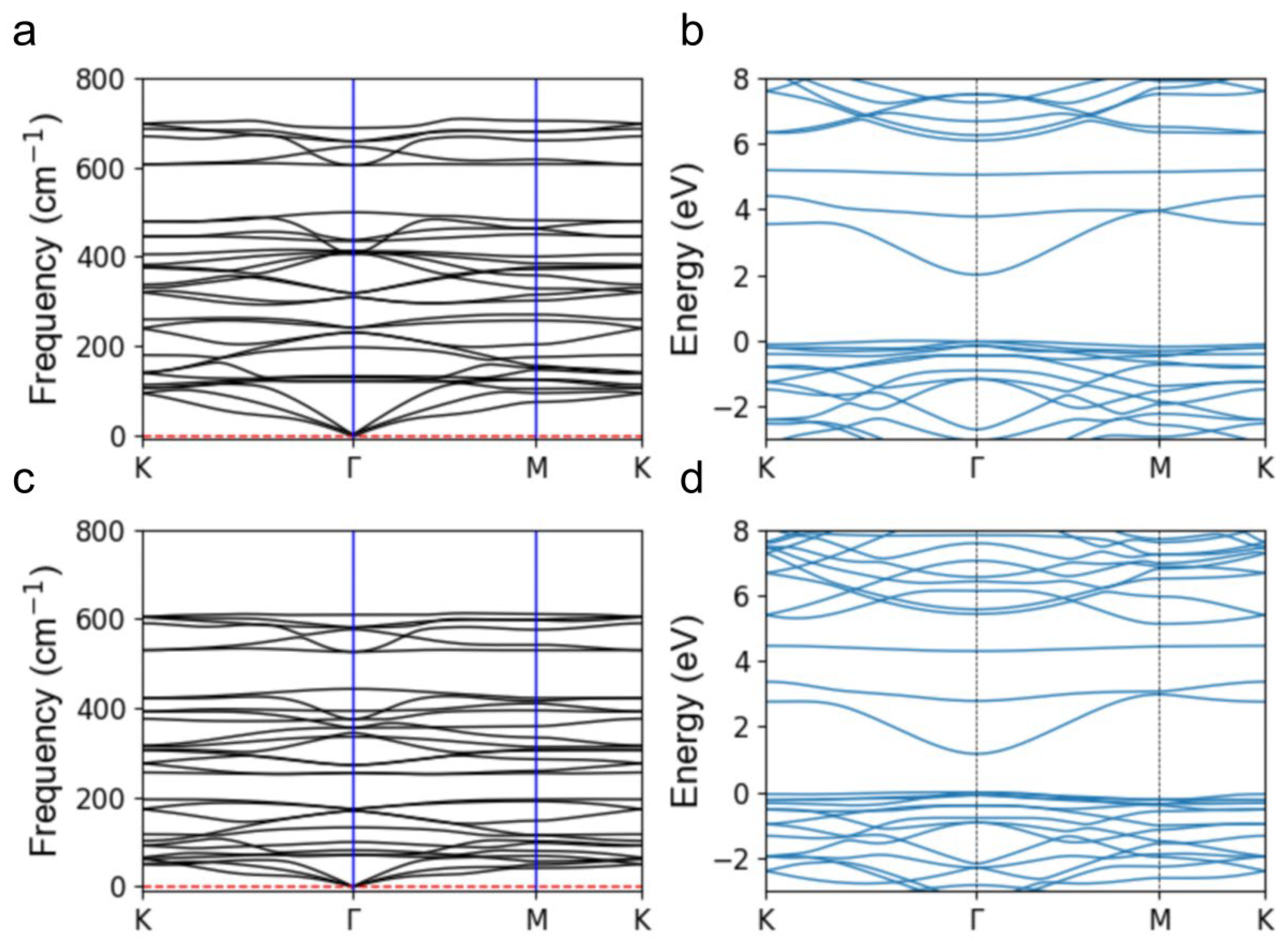
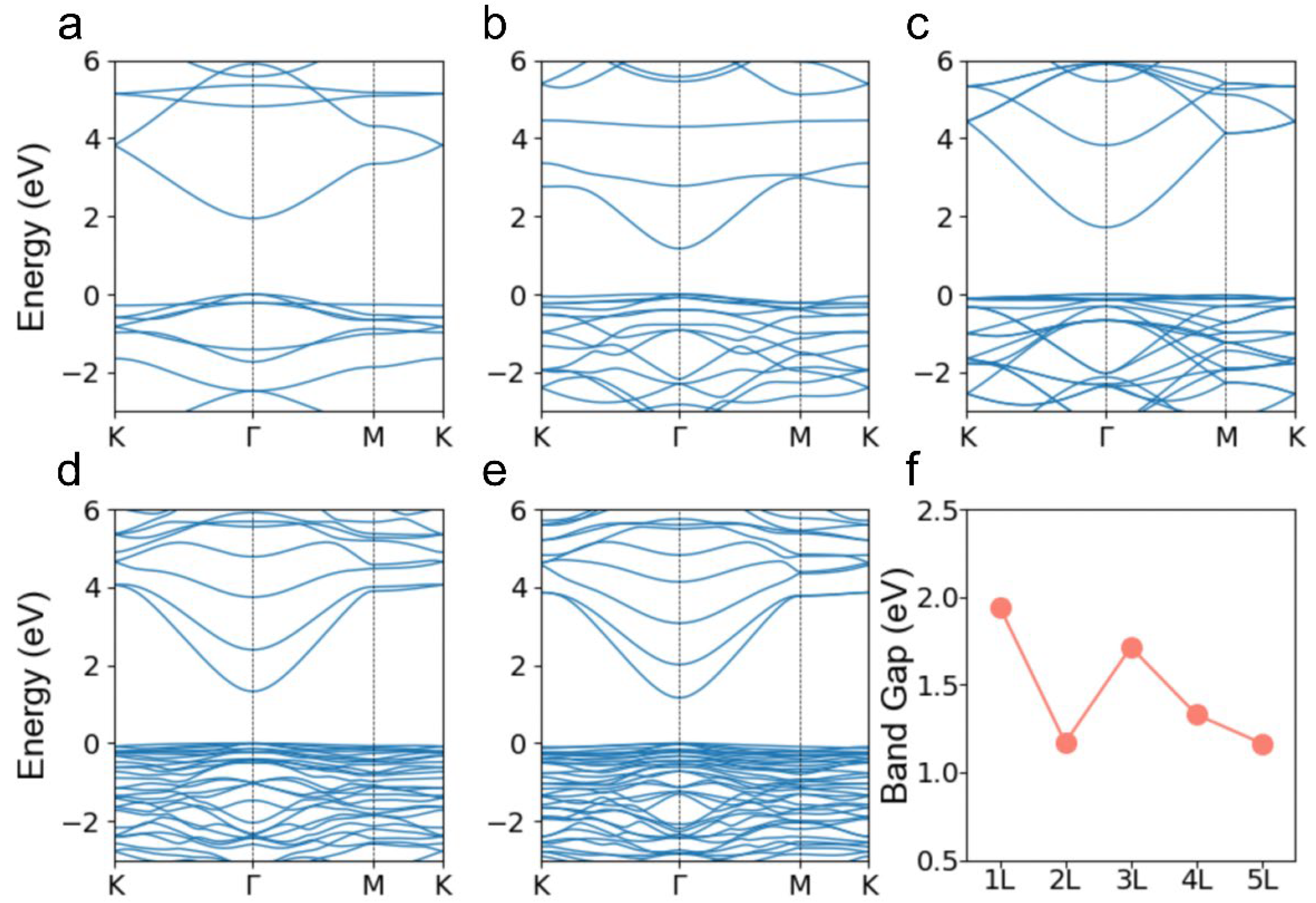
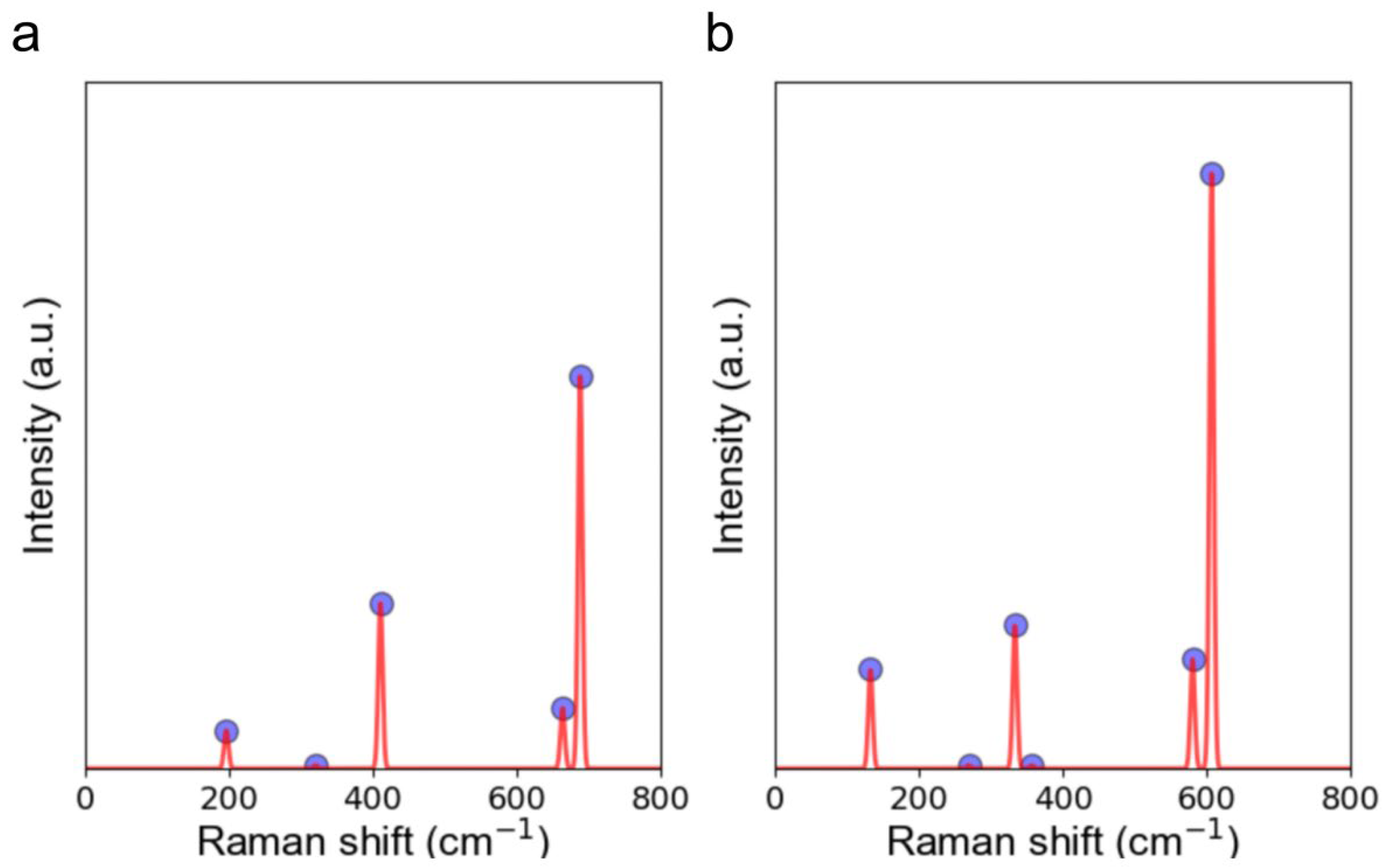
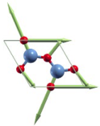
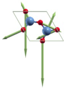
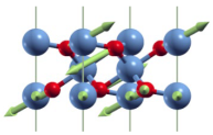
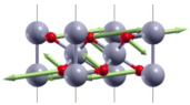
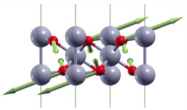
3. Results and Discussions
4. Conclusions
Author Contributions
Funding
Data Availability Statement
Conflicts of Interest
References
- Novoselov, K.S.; Geim, A.K.; Morozov, S.V.; Jiang, D.; Zhang, Y.; Dubonos, S.V.; Grigorieva, I.V.; Firsov, A.A. Electric field effect in atomically thin carbon films. Science 2004, 306, 666–669. [Google Scholar] [CrossRef] [PubMed]
- Chhowalla, M.; Shin, H.S.; Eda, G.; Li, L.J.; Loh, K.P.; Zhang, H. The chemistry of two-dimensional layered transition metal dichalcogenide nanosheets. Nat. Chem. 2013, 5, 263–275. [Google Scholar] [CrossRef] [PubMed]
- Huang, X.; Zeng, Z.; Zhang, H. Metal dichalcogenide nanosheets: Preparation, properties and applications. Chem. Soc. Rev. 2013, 42, 1934–1946. [Google Scholar] [CrossRef] [PubMed]
- Xu, M.; Liang, T.; Shi, M.; Chen, H. Graphene-like two-dimensional materials. Chem. Rev. 2013, 113, 3766–3798. [Google Scholar] [CrossRef] [PubMed]
- Jiang, J.; Guo, Y.; Weng, X.; Long, F.; Xin, Y.; Lu, Y.; Ye, Z.; Ruan, S.; Zeng, Y.-J. A tailorable polarity-flipping response in self-powered, flexible Sb2Se3/ZnO bilayer photodetectors. J. Mater. Chem. C 2021, 9, 4978–4988. [Google Scholar] [CrossRef]
- Dral, A.P.; ten Elshof, J.E. 2D metal oxide nanoflakes for sensing applications: Review and perspective. Sens. Actuators B Chem. 2018, 272, 369–392. [Google Scholar] [CrossRef]
- Huang, S.; Long, Y.; Ruan, S.; Zeng, Y.-J. Enhanced photocatalytic CO2 reduction in defect-engineered Z-scheme WO3-x/g-C3N4 heterostructures. ACS Omega 2019, 4, 15593–15599. [Google Scholar] [CrossRef]
- Jiao, S.; Fu, X.; Zhang, L.; Zeng, Y.-J.; Huang, H. Point-defect-optimized electron distribution for enhanced electrocatalysis: Towards the perfection of the imperfections. Nano Today 2020, 31, 100833. [Google Scholar] [CrossRef]
- Cakici, M.; Reddy, K.R.; Alonso-Marroquin, F. Advanced electrochemical energy storage supercapacitors based on the flexible carbon fiber fabric-coated with uniform coral-like MnO2 structured electrodes. Chem. Eng. J. 2017, 309, 151–158. [Google Scholar] [CrossRef]
- Al-Hardan, N.H.; Abdullah, M.J.; Ahmed, N.M.; Yam, F.K.; Aziz, A.A. UV photodetector behavior of 2D ZnO plates prepared by electrochemical deposition. Superlattices Microstruct. 2012, 51, 765–771. [Google Scholar] [CrossRef]
- Yin, Z.; Xu, K.; Jiang, S.; Luo, D.; Chen, R.; Xu, C.; Shum, P.; Liu, Y.J. Recent progress on two-dimensional layered materials for surface enhanced Raman spectroscopy and their applications. Mater. Today Phys. 2021, 18, 100378. [Google Scholar] [CrossRef]
- Singh, A.K.; Hennig, R.G. Computational prediction of two-dimensional group-IV mono-chalcogenides. Appl. Phys. Lett. 2014, 105, 042103. [Google Scholar] [CrossRef]
- Wang, Y.; Zhang, Q.; Shen, Q.; Cheng, Y.; Schwingenschlogl, U.; Huang, W. Lead monoxide: A two-dimensional ferromagnetic semiconductor induced by hole-doping. J. Mater. Chem. C 2017, 5, 4520–4525. [Google Scholar] [CrossRef]
- Daeneke, T.; Atkin, P.; Orrell-Trigg, R.; Zavabeti, A.; Ahmed, T.; Walia, S.; Liu, M.; Tachibana, Y.; Javaid, M.; Greentree, A.D.; et al. Wafer-scale synthesis of semiconducting SnO monolayers from interfacial oxide layers of metallic liquid tin. ACS Nano 2017, 11, 10974–10983. [Google Scholar] [CrossRef] [PubMed]
- Yan, B.; Zhou, P.; Xu, Q.; Zhou, X.; Xu, D.; Zhu, J. Engineering disorder into exotic electronic 2D TiO2 nanosheets for enhanced photocatalytic performance. RSC Adv. 2016, 6, 6133–6137. [Google Scholar] [CrossRef]
- Tao, J.; Luttrell, T.; Batzill, M. A two-dimensional phase of TiO2 with a reduced bandgap. Nat. Chem. 2011, 3, 296–300. [Google Scholar] [CrossRef]
- Addou, R.; Dahal, A.; Batzill, M. Growth of a two-dimensional dielectric monolayer on quasi-freestanding graphene. Nat. Nanotechnol. 2013, 8, 41–45. [Google Scholar] [CrossRef]
- Matsuzaki, K.; Hosono, H.; Susaki, T. Layer-by-layer epitaxial growth of polar MgO(111) thin films. Phys. Rev. B 2010, 82, 033408. [Google Scholar] [CrossRef]
- Sun, Z.; Liao, T.; Dou, Y.; Hwang, S.M.; Park, M.-S.; Jiang, L.; Kim, J.H.; Dou, S.X. Generalized self-assembly of scalable two-dimensional transition metal oxide nanosheets. Nat. Commun. 2014, 5, 3813. [Google Scholar] [CrossRef]
- Yang, M.; Ye, Z.; Iqbal, M.A.; Liang, H.; Zeng, Y.-J. Progress on two-dimensional binary oxide materials. Nanoscale 2022, 14, 9576–9608. [Google Scholar] [CrossRef]
- Lee, H.-Y.; Liu, J.-T.; Lee, C.-T. Modulated Al2O3-Alloyed Ga2O3 Materials and Deep Ultraviolet Photodetectors. IEEE Photon. Technol. Lett. 2018, 30, 549–552. [Google Scholar] [CrossRef]
- Liu, J.W.; Liao, M.Y.; Imura, M.; Banal, R.G.; Koide, Y. Deposition of TiO2/Al2O3 bilayer on hydrogenated diamond for electronic devices: Capacitors, field-effect transistors, and logic inverters. J. Appl. Phys. 2017, 121, 224502. [Google Scholar] [CrossRef]
- Chang, C.-W.; Kuo, C.-P. Evaluation of surface roughness in laser-assisted machining of aluminum oxide ceramics with Taguchi method. Int. J. Mach. Tools Manuf. 2007, 47, 141–147. [Google Scholar] [CrossRef]
- Komine, F.; Tomic, M.; Gerds, T.; Strub, J.R. Influence of different adhesive resin cements on the fracture strength of aluminum oxide ceramic posterior crowns. J. Prosthet. Dent. 2004, 92, 359–364. [Google Scholar] [CrossRef] [PubMed]
- Vekinis, G.; Ashby, M.F.; Beaumont, P.W.R. R-curbe behaviour of Al2O3 ceramics. Acta Metall. Mater. 1990, 38, 1151–1162. [Google Scholar] [CrossRef]
- Huang, Z.; Zhou, A.; Wu, J.; Chen, Y.; Lan, X.; Bai, H.; Li, L. Bottom-up preparation of ultrathin 2D aluminum oxide nanosheets by duplicating graphene oxide. Adv. Mater. 2016, 28, 1703–1708. [Google Scholar] [CrossRef]
- Ozyurt, A.K.; Molavali, D.; Sahin, H. Stable single layer structures of aluminum oxide: Vibrational and electronic characterization of magnetic phases. Comput. Mater. Sci. 2022, 214, 111745. [Google Scholar] [CrossRef]
- Hasan, S.R.; Abbas, Z.; Khan, M.S. The Al2O3-monolayer sensitivity towards NH3 and PH3 molecule: A DFT Study. J. Water Environ. Nanotechnol. 2023, 8, 31–40. [Google Scholar]
- Song, T.T.; Yang, M.; Chai, J.W.; Callsen, M.; Zhou, J.; Yang, T.; Zhang, Z.; Pan, J.S.; Chi, D.Z.; Feng, Y.P.; et al. The stability of aluminium oxide monolayer and its interface with two-dimensional materials. Sci. Rep. 2016, 6, 29221. [Google Scholar] [CrossRef]
- Chen, X.; Ren, F.; Gu, S.; Ye, J. Review of gallium-oxide-based solar-blind ultraviolet photodetectors. Photonics Res. 2019, 7, 381–415. [Google Scholar] [CrossRef]
- Dong, H.; Long, S.; Sun, H.; Zhao, X.; He, Q.; Qin, Y.; Jian, G.; Zhou, X.; Yu, Y.; Guo, W.; et al. Fast switching beta-Ga2O3 power MOSFET with a trench-gate Structure. IEEE Electron Device Lett. 2019, 40, 1385–1388. [Google Scholar] [CrossRef]
- Green, A.J.; Chabak, K.D.; Baldini, M.; Moser, N.; Gilbert, R.; Fitch, R.C., Jr.; Wagner, G.; Galazka, Z.; McCandless, J.; Crespo, A.; et al. Beta-Ga2O3 MOSFETs for radio frequency operation. IEEE Electron Device Lett. 2017, 38, 790–793. [Google Scholar] [CrossRef]
- Mukhopadhyay, P.; Schoenfeld, W.V. High responsivity tin gallium oxide Schottky ultraviolet photodetectors. J. Vac. Sci. Technol. A 2020, 38, 013403. [Google Scholar] [CrossRef]
- Zhang, D.; Du, Z.; Ma, M.; Zheng, W.; Liu, S.; Huang, F. Enhanced performance of solar-blind ultraviolet photodetector based on Mg-doped amorphous gallium oxide film. Vacuum 2019, 159, 204–208. [Google Scholar] [CrossRef]
- Manifacier, J.C.; Szepessy, L. Efficient sprayed In2O3:Sn n-type silicon heterojunction solar cell. Appl. Phys. Lett. 1977, 31, 459–462. [Google Scholar] [CrossRef]
- Hamberg, I.; Granqvist, C.G. Evaporated Sn-doped In2O3 films: Basic optical properties and applications to energy-efficient windows. J. Appl. Phys. 1986, 60, R123–R159. [Google Scholar] [CrossRef]
- Lee, J.S.; Kwack, Y.J.; Choi, W.S. Inkjet-printed In2O3 thin-film transistor below 200 degrees C. ACS Appl. Mater. Interfaces 2013, 5, 11578–11583. [Google Scholar] [CrossRef]
- Von Wenckstern, H.; Splith, D.; Schmidt, F.; Grundmann, M.; Bierwagen, O.; Speck, J.S. Schottky contacts to In2O3. APL Mater. 2014, 2, 046104. [Google Scholar] [CrossRef]
- Lee, D.; Seo, J. Graphene growth on sapphire via palladium silicidation. Appl. Surf. Sci. 2019, 492, 23–26. [Google Scholar] [CrossRef]
- Liu, H.; Chi, D. Dispersive growth and laser-induced rippling of large-area singlelayer MoS2 nanosheets by CVD on c-plane sapphire substrate. Sci. Rep. 2015, 5, 11756. [Google Scholar] [CrossRef]
- Thakur, D.; Sharma, M.; Balakrishnan, V.; Vaish, R. Reusable piezocatalytic water disinfection activity of CVD-grown few-layer WS2 on sapphire substrate. Environ. Sci. Nano 2022, 9, 805–814. [Google Scholar] [CrossRef]
- Yang, W.; Mu, Y.; Chen, X.; Jin, N.; Song, J.; Chen, J.; Dong, L.; Liu, C.; Xuan, W.; Zhou, C.; et al. CVD growth of large-area monolayer WS2 film on sapphire through tuning substrate environment and its application for high-sensitive strain sensor. Nanoscale Res. Lett. 2023, 18, 13. [Google Scholar] [CrossRef] [PubMed]
- Balan, A.P.; Radhakrishnan, S.; Woellner, C.F.; Sinha, S.K.; Deng, L.; de los Reyes, C.; Rao, B.M.; Paulose, M.; Neupane, R.; Apte, A.; et al. Exfoliation of a non-van der Waals material from iron ore hematite. Nat. Nanotechnol. 2018, 13, 602–609. [Google Scholar] [CrossRef] [PubMed]
- Giannozzi, P.; Andreussi, O.; Brumme, T.; Bunau, O.; Nardelli, M.B.; Calandra, M.; Car, R.; Cavazzoni, C.; Ceresoli, D.; Cococcioni, M.; et al. Advanced capabilities for materials modelling with QUANTUM ESPRESSO. J. Phys. Condens. Matter 2017, 29, 465901. [Google Scholar] [CrossRef]
- Giannozzi, P.; Baroni, S.; Bonini, N.; Calandra, M.; Car, R.; Cavazzoni, C.; Ceresoli, D.; Chiarotti, G.L.; Cococcioni, M.; Dabo, I.; et al. QUANTUM ESPRESSO: A modular and open-source software project for quantum simulations of materials. J. Phys. Condens. Matter 2009, 21, 395502. [Google Scholar] [CrossRef]
- Perdew, J.P.; Burke, K.; Ernzerhof, M. Generalized gradient approximation made simple. Phys. Rev. Lett. 1996, 77, 3865–3868. [Google Scholar] [CrossRef]
- Monkhorst, H.J.; Pack, J.D. Special points for Brillouin-zone integrations. Phys. Rev. B 1976, 13, 5188–5192. [Google Scholar] [CrossRef]
- Baroni, S.; de Gironcoli, S.; Dal Corso, A.; Giannozzi, P. Phonons and related crystal properties from density-functional perturbation theory. Rev. Mod. Phys. 2001, 73, 515–562. [Google Scholar] [CrossRef]
- Santos, R.C.R.; Longhinotti, E.; Freire, V.N.; Reimberg, R.B.; Caetano, E.W.S. Elucidating the high-k insulator alpha-Al2O3 direct/indirect energy band gap type through density functional theory computations. Chem. Phys. Lett. 2015, 637, 172–176. [Google Scholar] [CrossRef]
- Pham, A.; Assadi, M.H.N.; Yu, A.B.; Li, S. Critical role of Fock exchange in characterizing dopant geometry and magnetic interaction in magnetic semiconductors. Phys. Rev. B 2014, 89, 155110. [Google Scholar] [CrossRef]
- Sousa, S.F.; Fernandes, P.A.; Ramos, M.J. General performance of density functionals. J. Phys. Chem. A 2007, 111, 10439–10452. [Google Scholar] [CrossRef] [PubMed]


| Before Optimization | After Optimization | Ef (eV) | |
|---|---|---|---|
| Type Ⅰ |  |  | 3.78 |
| Type Ⅱ | 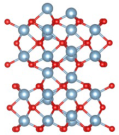 |  | 15.12 |
| Mode | Frequency (cm−1) | Top View |
|---|---|---|
| A′1 | 387 |  |
| E′(1) | 754 |  |
 | ||
| E′(2) | 1043 | 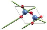 |
 |
| Mode | Frequency (cm−1) | Side View |
|---|---|---|
| A1g(1) | 367 |  |
| A1g(2) | 521 | 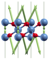 |
| Eg(1) | 554 | 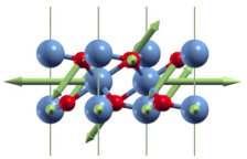 |
 | ||
| A1g(3) | 797 |  |
| Eg(2) | 881 |  |
 |
| Mode | Frequency (cm−1) | Side View |
|---|---|---|
| A1g(1) | 196 | 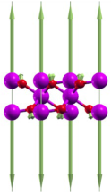 |
| Eg(1) | 320 |  |
 | ||
| A1g(2) | 410 | 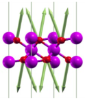 |
| Eg(2) | 664 | 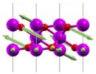 |
 | ||
| A1g(3) | 689 | 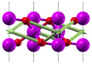 |
| Mode | Frequency (cm−1) | Side View |
|---|---|---|
| A1g(1) | 133 | 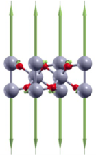 |
| Eg(1) | 269 |  |
 | ||
| A1g(2) | 333 | 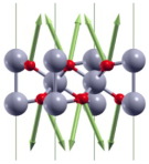 |
| Eg(2) | 357 |  |
 | ||
| Eg(3) | 580 | 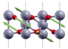 |
 | ||
| A1g(3) | 607 |  |
Disclaimer/Publisher’s Note: The statements, opinions and data contained in all publications are solely those of the individual author(s) and contributor(s) and not of MDPI and/or the editor(s). MDPI and/or the editor(s) disclaim responsibility for any injury to people or property resulting from any ideas, methods, instructions or products referred to in the content. |
© 2023 by the authors. Licensee MDPI, Basel, Switzerland. This article is an open access article distributed under the terms and conditions of the Creative Commons Attribution (CC BY) license (https://creativecommons.org/licenses/by/4.0/).
Share and Cite
Zhou, Y.; Zhu, J.; Cai, D.; Cheng, Y. The Possibility of Layered Non-Van Der Waals Boron Group Oxides: A First-Principles Perspective. Crystals 2023, 13, 1298. https://doi.org/10.3390/cryst13091298
Zhou Y, Zhu J, Cai D, Cheng Y. The Possibility of Layered Non-Van Der Waals Boron Group Oxides: A First-Principles Perspective. Crystals. 2023; 13(9):1298. https://doi.org/10.3390/cryst13091298
Chicago/Turabian StyleZhou, Yu, Jun Zhu, Dongyu Cai, and Yingchun Cheng. 2023. "The Possibility of Layered Non-Van Der Waals Boron Group Oxides: A First-Principles Perspective" Crystals 13, no. 9: 1298. https://doi.org/10.3390/cryst13091298
APA StyleZhou, Y., Zhu, J., Cai, D., & Cheng, Y. (2023). The Possibility of Layered Non-Van Der Waals Boron Group Oxides: A First-Principles Perspective. Crystals, 13(9), 1298. https://doi.org/10.3390/cryst13091298