Article

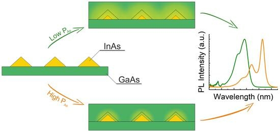
Influence of the Arsenic Pressure during Rapid Overgrowth of InAs/GaAs Quantum Dots on Their Photoluminescence Properties

1
Laboratory of Epitaxial Technologies, Institute of Nanotechnologies, Electronics and Equipment Engineering, Southern Federal University, 347922 Taganrog, Russia
2
International Laboratory of Quantum Optoelectronics, HSE University, 190008 St. Petersburg, Russia
*
Authors to whom correspondence should be addressed.
Crystals 2023, 13(9), 1358; https://doi.org/10.3390/cryst13091358
Submission received: 6 August 2023 / Revised: 4 September 2023 / Accepted: 5 September 2023 / Published: 8 September 2023
(This article belongs to the Special Issue Epitaxial Growth of Semiconductor Materials and Devices)

Abstract

:
In this paper, for the first time, we report a strong effect of the arsenic pressure used for the high-rate GaAs capping of self-assembled InAs quantum dots on their optical properties. A 140 nm red shift of the photoluminescence peak position is observed when the overgrowth arsenic pressure increases threefold. We explain this behavior in terms of different intensities of quantum dot decomposition, which occurs during the overgrowth under different conditions. When the arsenic pressure is sufficiently high, a GaAs capping layer is formed by deposited species with a low impact on initial quantum dots. At a low arsenic pressure, arsenic deficiency leads to the intensive intermixing caused both by the enhanced Ga/In atom exchange and by the consumption of arsenic atoms belonging to quantum dots for the GaAs capping layer formation. As a result of the overgrowth, quantum dots are divided into families with a large (high pressure) and a small (low pressure) average size, yielding long-wave (1.23 µm) and short-wave (1.09 µm) photoluminescence peaks, respectively. Thus, a significant influence of the overgrowth arsenic pressure on the characteristics of InAs quantum dots is evidenced in this study.

Graphical Abstract

1. Introduction

Optoelectronic devices based on semiconductor quantum dots (QDs) have been attracting significant attention due to numerous advantages resulting from their atomic-like energy spectrum [1,2,3]. Lasers based on InAs/GaAs QDs exhibit low threshold current density, high gain, high characteristic temperature and many more virtues [4,5]. Moreover, they can emit at telecom wavelengths benefiting from the low propagation losses in the widely used silica fibers [6,7]. To provide high internal quantum efficiency of the lasers, the qualitative growth of QDs is a necessary but not a sufficient condition. A crucial effect on the geometrical parameters and emission properties of QDs is often exerted by their capping with a wide-gap matrix. It is commonly known that the overgrowth of QDs results in the drastic change in QDs’ size and shape due to the processes of segregation, intermixing, etc. [8,9]. A decrease in the height of QDs leads to a blue shift of their emission wavelength, as compared to the uncapped QDs [10]. To shift the emission wavelength towards the O-band, InGaAs strain-reducing layer can be used instead of GaAs [11,12,13,14]. However, high concentration of In atoms in QDs and the capping layer induces non-radiative recombination centers, which deteriorate the optical quality of QDs [15]. The fabrication of QD heterostructures emitting in the C-band is even more challenging. InP substrates are traditionally used to grow lattice-matched InGaAlAs layers with a precise composition and embed InAs QDs between them to obtain emission around 1.55 µm [16]. However, InP-based QD technology is still inferior to GaAs in terms of characteristics such as available wafer sizes, thermal conductivity, band offsets, refractive index contrast and a possibility of producing high-quality distributed Bragg reflectors [15,17].
Standard GaAs capping of InAs QDs has been also thoroughly investigated recently [18,19,20]. It was found that a high overgrowth temperature leads to decomposition and dissolution of QDs [21], whereas a reduction in the temperature relative to the QD growth induces defect formation and degradation of optical quality of QDs [13]. QD capping at low growth rates was found to enhance In segregation and intermixing, leading to a blue shift in the photoluminescence (PL) spectra [18,20]. Furthermore, an energy gap between a ground and a first excited state is smaller for QDs overgrown at lower rates, which increases the probability of lasing from excited states when this structure is used in laser devices [11]. Meanwhile, high overgrowth rates allow better preservation of the QD size and shape, resulting in large emission wavelengths [18,20,22]. Numerous studies have been devoted to the growth of InAs QDs under different arsenic vapor pressures, leading to a change in both morphological parameters of QDs and their photoluminescence properties [23,24,25]. Surprisingly, an influence of the arsenic pressure used for the overgrowth of InAs QDs on their structural and optical properties is rarely mentioned in the literature. Nevertheless, it may have a critical effect on the capping processes when it is necessary to provide high PL intensity at wavelengths of 1.3 and 1.55 µm. In particular, a strong dependence of the PL spectra of InAs/GaAs QD heterostructures on the arsenic pressure used for the slow-rate overgrowth was demonstrated previously [19]. This factor is especially important when we consider that the widespread use of QD technology for the production of lasers and other optoelectronic devices is hindered by the poor reproducibility of QD parameters [26]. In addition to the fact that it is associated with their sensitivity to fluctuations in the growth conditions, a significant role is also played by the neglect of the significance of the arsenic pressure influence during QD overgrowth.
In this paper, we reveal a crucial effect of the arsenic pressure during low-temperature GaAs/InAs rapid overgrowth on the PL properties of QDs. A role of the arsenic concentration in the near-surface layer during the overgrowth is discussed. PL spectra exhibit a strong blue shift of the PL peak position with decreasing overgrowth pressure, which is attributed to the enhancement of QD decomposition caused by the deficiency of arsenic species.

2. Materials and Methods
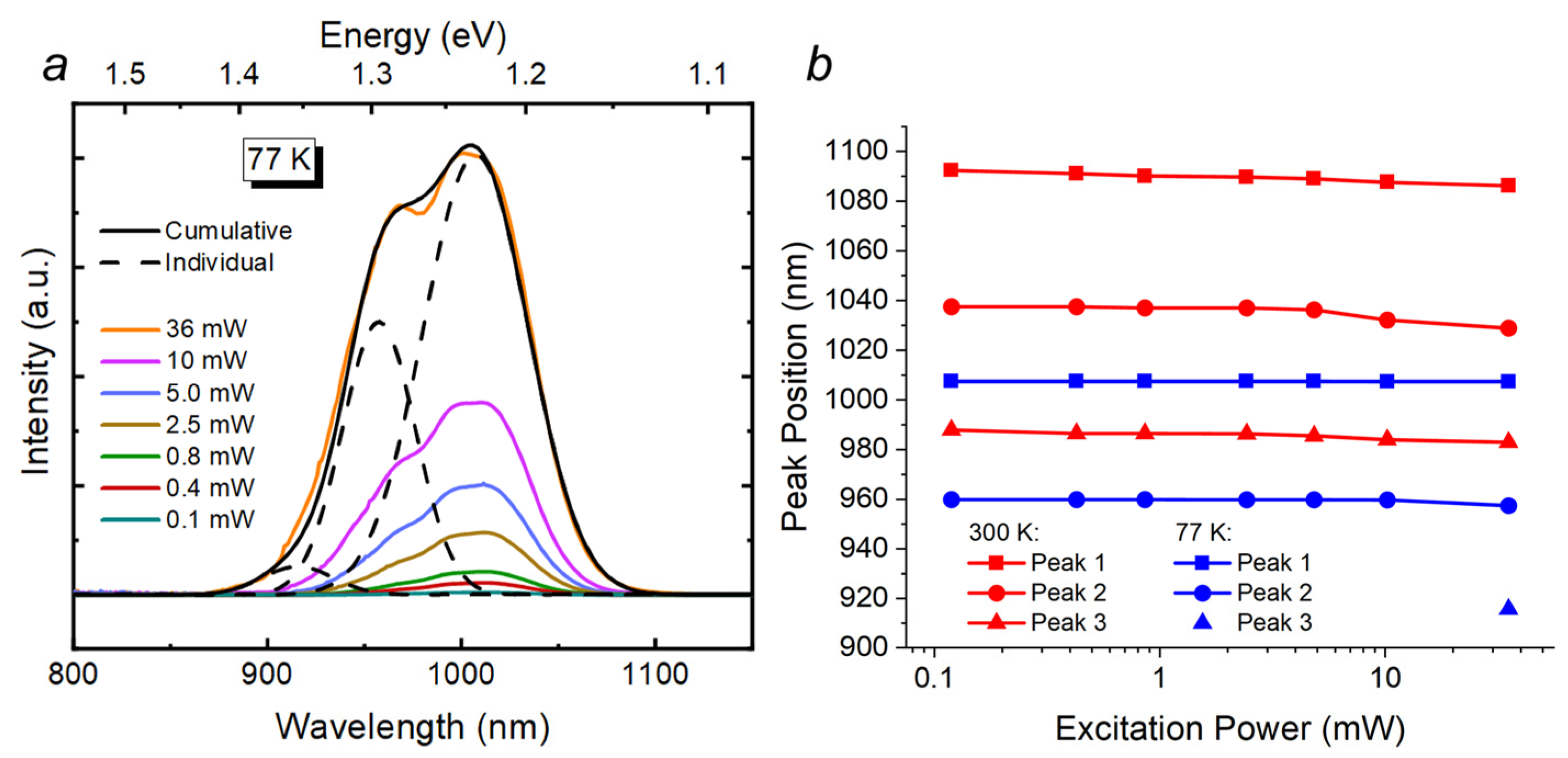
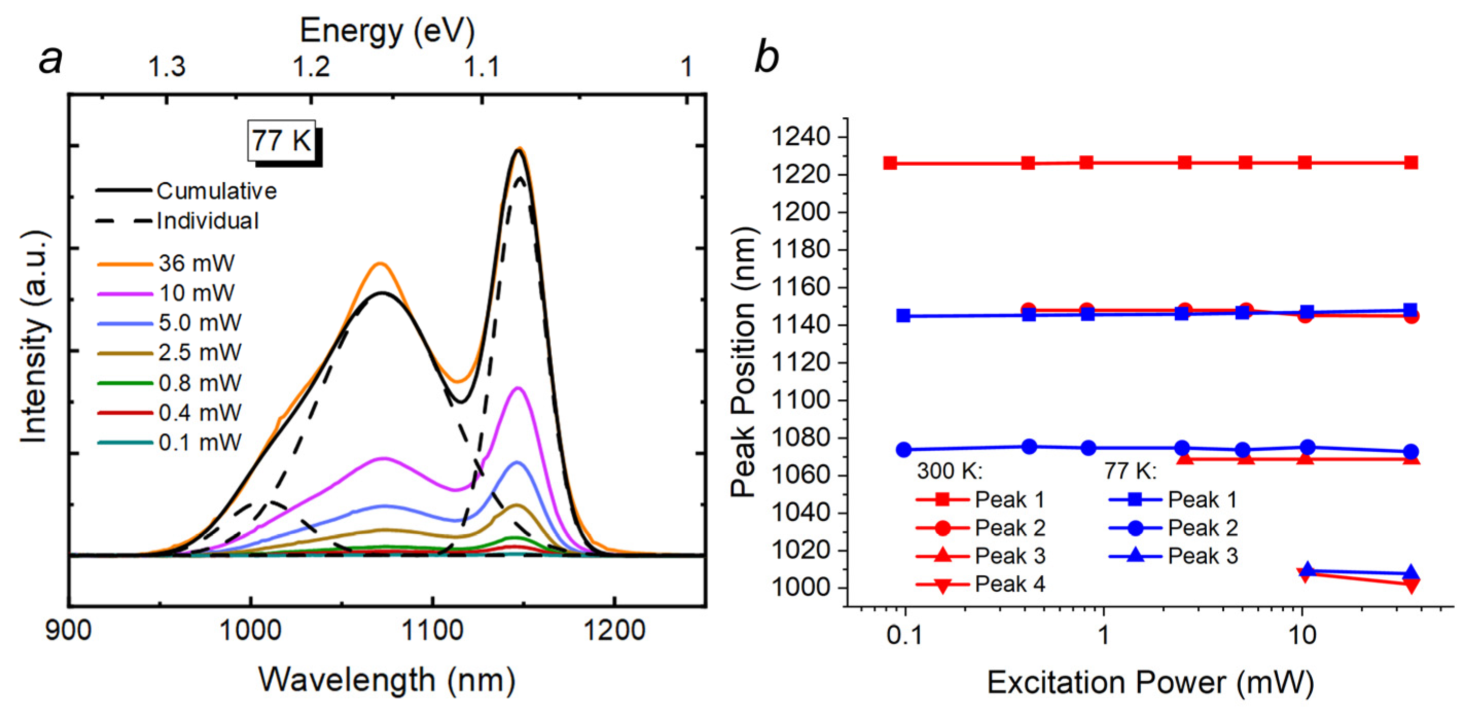
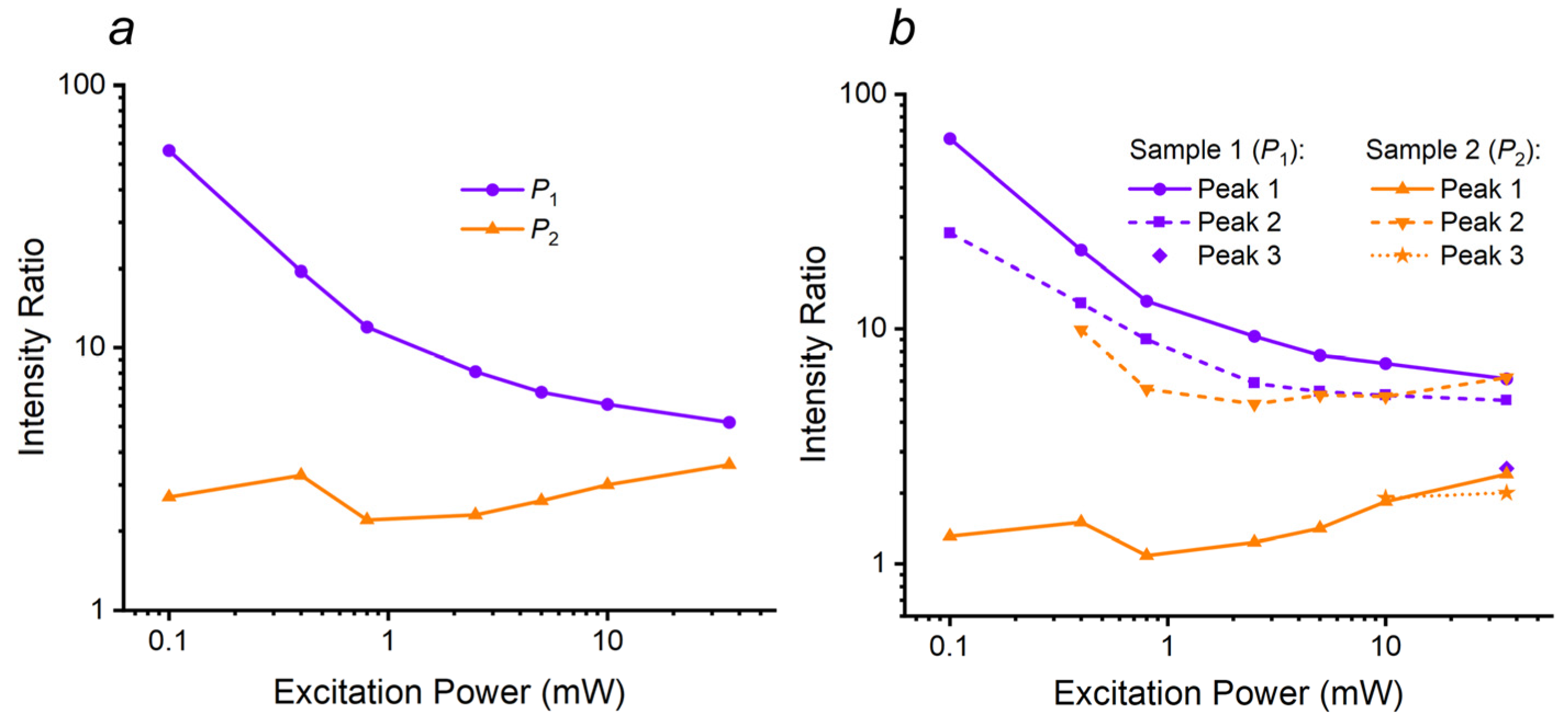
SemiTEq STE 35 molecular beam epitaxy equipment with solid-state (group III and As) sources was used to grow all samples on semi-insulating GaAs(001) epi-ready substrates. After a standard deoxidization procedure at 600 °C under an arsenic pressure of 4 × 10⁻⁵ Pa during 15 min, a 250 nm GaAs buffer layer was grown at 580 °C. QDs were formed after deposition of 2.5 monolayers (ML) InAs on a GaAs surface at a substrate temperature of 500 °C, a growth rate of 0.05 ML/s and an arsenic pressure of 1 × 10⁻⁵ Pa. The 2D–3D transition during QD formation was registered in situ by reflection high-energy electron diffraction. The QDs in sample 0 were grown directly on the buffer layer without subsequent capping for studies using scanning electron microscopy (SEM). QDs were embedded in a heterostructure containing 100 nm-thick inner GaAs layers and 50 nm-thick Al0.33Ga0.67As outer layers for further PL studies. First, 10 nm of the capping GaAs layer was grown at 500 °C and 1 ML/s under different arsenic pressures: P1 = 1 × 10⁻⁵ Pa (sample 1) and P2 = 3 × 10⁻⁵ Pa (sample 2). A 10 nm-thick GaAs capping layer was grown on top of the Al0.33Ga0.67As cladding layer, followed by annealing of the sample at 610 °C to reduce the number of defects. All GaAs and AlGaAs layers were grown at 580 °C and 600 °C, respectively.
PL studies were carried out in a flow Janis ST-500 cryostat, which allowed measurements in the temperature range from 77 to 300 K. A YLF:Nd+3 laser operating in the cw mode (λ = 527 nm) was used to excite PL in the analyzed samples. The excitation power varied in the range 0.1–36 mW. Laser radiation was focused onto the sample surface using a Mitutoyo ×5 objective to a 20 μm-diameter spot. The PL signal was detected with a SOL Instruments MS 5204i monochromator and a single-channel InGaAs detector using synchronous detection (SRS 830 Stanford Research Systems).

3. Results

A SEM image of uncapped QDs and their lateral size distribution is presented in Figure 1a and 1b, respectively. Two representative size groups of QDs with an average diameter of 22 and 40 nm can be seen in Figure 1a. The first one represents regular QDs with a surface density of 4 × 1010 cm−2. The second size group with a density of 3 × 108 cm−2 is associated with QD coalescence, which occurs during the formation and ripening of InAs islands [27,28]. The full width at half maximum (FWHM) of the Gaussian curve approximating the size distribution histogram is 9 nm (Figure 1b), with a standard diameter deviation of 14%.
Next, 77 K PL spectra of the sample 1 with QDs overgrown at a low arsenic pressure are presented in Figure 2a. Despite the fact that the size distribution of uncovered QDs is unimodal (Figure 1b), two peaks are clearly observed in the PL spectra of the overgrown sample (Figure 2a). According to the deconvolution results, two PL peaks at a wavelengths of 1007 and 960 nm can be distinguished for the measurements at 77 K in the entire range of excitation powers (1086 and 1029 nm at 300 K, Figure 2b). The presence of the peak 2 (960 nm) at low excitation powers suggests that this PL line represents a ground state contribution of QDs [29] as well as the peak 1 PL line. However, these PL lines are contributed by QDs belonging to different size groups. A ratio of the integrated intensities of these two PL contributions at 77 K ranges from 14.2 (at an excitation power of 0.1 mW) to 2.3 (at an excitation power of 36 mW). This cannot be addressed to PL contributions of regular and coalescent QDs because the ratio of their surface densities is more than 130. Consequently, QD families with different representative sizes appear after the capping procedure, which was already observed in previous works [10,30].
Figure 2b also demonstrates that a third peak at 916 nm appears in the spectra at an excitation power of 36 mW in the case of PL measurements at 77 K. We believe that this contribution refers to a new branch of QD sizes rather than to an excited state because PL spectra taken at 300 K show that a third peak at 983 nm exists in the entire range of excitation powers (Figure 2b). A FWHM of Gaussian curves approximating PL contributions of the peaks 1, 2 and 3 at 77 K are 71, 66 and 53 meV, respectively, for an excitation power of 36 mW. The energy intervals between the PL peak positions are ~60 meV.
Figure 3a presents 77 K PL spectra of sample 2 with the high-pressure overgrowth of QDs. Again, two PL peaks at 1148 and 1073 nm corresponding to different QD size families are identified. Analysis of the deconvoluted spectra demonstrates that a third peak at a wavelength of 1008 nm appears at 10 mW as an excited state of QDs (Figure 3b). One more excited state can be observed in the spectra taken at 300 K. In this case, four PL peaks are located at wavelengths of 1226, 1145 (starting from 0.4 mW), 1069 (from 2.5 mW) and 1002 nm (from 10 mW). The first longwave line has a FWHM of 31 meV for the 77 K spectrum and 37 meV for the 300 K spectrum at an excitation power of 36 mW, which is in a traditional range of narrow PL linewidths of InAs/GaAs QDs [24,31]. These values may indicate very high uniformity of QD sizes within the branch of large QDs. The next line with a peak at 1073 nm is three times broader, with a FWHM of 90 meV at 77 K (36 mW). In the 300 K spectrum, this line is narrower with a FWHM of 64 meV (36 mW) because recombination of charge carries is assumed to occur through a smaller number of QDs with the most favorable energy states. The energy interval between the first and the second PL peaks of the sample 2 is 75 meV, which is larger than that of the sample 1 and allows better temperature stability of optoelectronic devices based on the sample 2-type QDs.

4. Discussion

Normalized PL spectra of both samples at different PL measurement temperatures are shown in Figure 4. A position of the PL intensity maximum is observed to shift from 1086 to 1226 nm at 300 K (from 1007 to 1148 nm at 77 K) when the overgrowth arsenic pressure is increased from P1 to P2. This is attributed to the strong influence of the arsenic pressure on the atomistic processes occurring in the heteroepitaxial system. Overgrowth of QDs by a layer of lattice-mismatched material leads to QD decomposition induced by intermixing and segregation processes [9,32]. Depending on the overgrowth conditions, QD size and shape can be well-conserved or significantly changed [8,33]. According to the PL spectra analyzed in this study, a decrease in the arsenic pressure during overgrowth leads to a 140 nm blue shift of the PL intensity peak position. This indicates a reduction in the QD size with increasing overgrowth rate due to their more intensive decomposition. When the capping process begins, an equilibrium state established between QDs and the underlying GaAs layer is broken, which leads to the search for a new equilibrium state. The “QD–matrix” system tends to minimize the energy, including the strain energy that arises between lattice mismatched materials. This is most easily achieved by mixing the materials, i.e., depriving initial QDs of a part of indium atoms. At a flux ratio corresponding to a pressure of 3 × 10⁻⁵ Pa, a balance of group-III and group-V species is observed in the system when the diffusion gradient from QDs into the capping layer is not very high. In this case, the size of initial QDs is better preserved. At a pressure of 1 × 10⁻⁵ Pa, the As/Ga flux ratio abruptly decreases so that the QD decomposition becomes more influenced by the Ga flux rather than the As flux. In this case, gallium acts as a drain for arsenic atoms belonging to QDs, leading to a violation of the stoichiometric balance within the QD and to its more intensive decomposition. Furthermore, excess Ga atoms can be more actively incorporated into QDs, replacing larger In atoms, which results in the QD decomposition and a decrease in their emission wavelength.
Besides a reduction in size of a QD as a consequence of the exchange of Ga and In atoms, significant fluctuations in the In fraction occurs in the QD vicinity. According to various studies using transmission electron microscopy with an energy-dispersive X-ray system and cross-sectional scanning tunneling microscopy, intermixing of QDs and a capping layer leads to an increase in the wetting layer thickness from ~1.4 ML up to 5 nm [18,20,34] and to a decrease in the In fraction within an initial QD area from nearly 100% to 33% [32]. Naturally, this leads to blurring of the heterointerface between a QD and the surrounding wide-gap matrix. Numerical calculations for two different shapes of InAs potential wells demonstrated that a difference between energy levels in a parabolic well is larger than in a rectangular well [35], which may be an additional reason why QDs overgrown at a smaller arsenic pressure emit at shorter wavelengths.
Figure 5a shows the dependences of the ratio of integrated PL intensities at 77 K to 300 K against the excitation power. Sample 2 with QDs overgrown at P2 yields an increasing dependence of the 77/300 K PL intensity ratio varying in the range from 1.5 to 3.4. A small difference between the 77 and 300 K PL intensities is an indication of the good quality of the QD structure and strong localization of charge carriers in QDs. Meanwhile, the PL spectra of QDs overgrown at P1 taken at different temperatures vary in intensity much more significantly. The ratios of 77/300 K PL intensities are in the range from 55.3 to 5.7, which is up to 37 times larger than for the P2 counterpart. This behavior may be attributed to two phenomena. The first of them is associated with the ejection of charge carriers into the wide-gap matrix because the energy states in the sample 1 QDs are located closer to the GaAs level than those in sample 2. The second possible reason is a large number of defects in the sample 1 which hinder radiative recombination of charge carriers more intensively at a higher temperature because of their enhanced mobility. These defects may be of a stoichiometric nature due to the As/Ga flux imbalance during the rapid overgrowth.
An analysis of the 77/300 K intensity ratios shows that QDs of various size families in sample 1 make approximately the same contribution to the defectivity of the whole structure because separate PL contributions closely repeat the “intensity ratio—excitation power” dependence of the whole spectra (Figure 5b). At the same time, separate PL peaks of sample 2 demonstrate different behavior depending on the PL measurement temperature. A dependence of peak 1 located at a wavelength of 1226 nm (300 K) runs along the dependence of the whole spectra, whereas a peak 3 dependence lies higher and indicates worse quality of the QD structure. We believe that this is associated with higher defectivity of smaller-sized QDs. This is in good agreement with a larger FWHM of these QDs, implying that a part of them underwent more significant decomposition with the accompanying appearance of stoichiometric defects. A ratio of the integrated intensities of peak 1 to peak 2 both at 77 K and 300 K exceeds one: from 1.9 to 1.4 and from 5.5 to 2.1, respectively, for the excitation power range of 0.4–36 mW. Although it would indicate a larger number of smaller-defective large-sized QDs emitting at a wavelength of 1226 nm at 300 K, a ratio of the integrated intensities leaves this aspect ambiguous because it is less than one at 77 K: from 0.9 to 0.5. Nevertheless, a range of this ratio values from 3.8 to 2.4 at 300 K allows us to hope that sample 2 contains a sufficiently large number of homogeneous high-quality QDs capable of generating laser radiation near the telecommunication O-band.

5. Conclusions

Thus, InAs QDs with initial unimodal size distribution were found to divide into several branches with various characteristics after rapid GaAs capping. Depending on the arsenic pressure during the overgrowth, PL spectra may exhibit short-wave (low-pressure) and long-wave (high-pressure) peaks which indicate the presence of smaller and larger QD families, respectively. We attribute this behavior to different intensities of QD decomposition occurring during the overgrowth under different arsenic pressures. At high pressure, arsenic species bind to the deposited gallium so that a close-to-stoichiometric GaAs capping layer could be formed. When the arsenic pressure is significantly reduced, arsenic deficiency leads to the intensive intermixing caused both by the consumption of QD arsenic atoms for the GaAs capping layer formation and by the abundant incorporation of small Ga atoms into In vacancies in QDs (Ga/In atom exchange). Subsequently, QDs overgrown at the low-arsenic pressure decompose more significantly and emit at 140 nm-shorter wavelengths.
The results of this study highlight the need for careful selection of the arsenic pressure used during rapid capping of InAs/GaAs QDs. We believe that taking this factor into account will significantly advance QD technology, both in terms of understanding the overgrowth processes and in terms of ensuring good reproducibility of the device parameters.

Author Contributions

Conceptualization, S.B. and M.S.; methodology, S.B. and M.S.; validation, S.B., N.K., A.Z. and M.S.; formal analysis, S.B., N.K. and M.S.; investigation, S.B., D.K., N.C., N.S., S.K., A.D., N.K. and M.S.; resources, N.K., A.Z. and M.S.; writing—original draft preparation, S.B. and M.S.; writing—review and editing, S.B., N.K., A.Z. and M.S.; visualization, S.B., D.K. and M.S.; supervision, M.S.; project administration, N.K., A.Z. and M.S.; funding acquisition, N.K., A.Z. and M.S. All authors have read and agreed to the published version of the manuscript.

Funding

This research was funded by the Ministry of Science and Higher Education of the Russian Federation (Grant No. FENW-2022-0034) at the Southern Federal University and by the project “Mirror Laboratories”, HSE University, RF. Optical measurements were carried out on a USI “Complex Optoelectronic Stand”.

Data Availability Statement

Not applicable.

Conflicts of Interest

The authors declare no conflict of interest. The funders had no role in the design of the study; in the collection, analyses, or interpretation of data; in the writing of the manuscript; or in the decision to publish the results.

References

  1. Pryor, C. Geometry and Material Parameter Dependence of InAs/GaAs Quantum Dot Electronic Structure. Phys. Rev. B 1999, 60, 2869–2874. [Google Scholar] [CrossRef]
  2. Johansen, J.; Stobbe, S.; Nikolaev, I.S.; Lund-Hansen, T.; Kristensen, P.T.; Hvam, J.M.; Vos, W.L.; Lodahl, P. Size Dependence of the Wavefunction of Self-Assembled InAs Quantum Dots from Time-Resolved Optical Measurements. Phys. Rev. B-Condens. Matter Mater. Phys. 2008, 77, 073303. [Google Scholar] [CrossRef]
  3. Li, S.Y.; He, L. Recent Progresses of Quantum Confinement in Graphene Quantum Dots. Front. Phys. 2022, 17, 33201. [Google Scholar] [CrossRef]
  4. Bimberg, D.; Ledentsov, N. Quantum Dots: Lasers and Amplifiers. J. Phys. Condens. Matter 2003, 15, R1063–R1076. [Google Scholar] [CrossRef]
  5. Ledentsov, N.N.; Kovsh, A.R.; Zhukov, A.E.; Maleev, N.A.; Mikhrin, S.S.; Vasil’ev, A.P.; Semenova, E.S.; Maximov, M.V.; Shernyakov, Y.M.; Kryzhanovskaya, N.V.; et al. High Performance Quantum Dot Lasers on GaAs Substrates Operating in 1.5 µm Range. Electron. Lett. 2003, 39, 1126. [Google Scholar] [CrossRef]
  6. Zhao, T.M.; Chen, Y.; Yu, Y.; Li, Q.; Davanco, M.; Liu, J. Advanced Technologies for Quantum Photonic Devices Based on Epitaxial Quantum Dots. Adv. Quantum Technol. 2020, 3, 1900034. [Google Scholar] [CrossRef]
  7. García de Arquer, F.P.; Talapin, D.V.; Klimov, V.I.; Arakawa, Y.; Bayer, M.; Sargent, E.H. Semiconductor Quantum Dots: Technological Progress and Future Challenges. Science 2021, 373, eaaz8541. [Google Scholar] [CrossRef]
  8. Costantini, G.; Rastelli, A.; Manzano, C.; Acosta-Diaz, P.; Songmuang, R.; Katsaros, G.; Schmidt, O.G.; Kern, K. Interplay between Thermodynamics and Kinetics in the Capping of InAs/GaAs(001) Quantum Dots. Phys. Rev. Lett. 2006, 96, 226106. [Google Scholar] [CrossRef]
  9. García, J.M.; Medeiros-Ribeiro, G.; Schmidt, K.; Ngo, T.; Feng, J.L.; Lorke, A.; Kotthaus, J.; Petroff, P.M. Intermixing and Shape Changes during the Formation of InAs Self-Assembled Quantum Dots. Appl. Phys. Lett. 1997, 71, 2014–2016. [Google Scholar] [CrossRef]
  10. Ferdos, F.; Wang, S.; Wei, Y.; Larsson, A.; Sadeghi, M.; Zhao, Q. Influence of a Thin GaAs Cap Layer on Structural and Optical Properties of InAs Quantum Dots. Appl. Phys. Lett. 2002, 81, 1195–1197. [Google Scholar] [CrossRef]
  11. Hospodková, A.; Hulicius, E.; Pangrác, J.; Oswald, J.; Vyskočil, J.; Kuldová, K.; Šimeček, T.; Hazdra, P.; Caha, O. InGaAs and GaAsSb Strain Reducing Layers Covering InAs/GaAs Quantum Dots. J. Cryst. Growth 2010, 312, 1383–1387. [Google Scholar] [CrossRef]
  12. Trevisi, G.; Suárez, I.; Seravalli, L.; Rivas, D.; Frigeri, P.; Muñoz-Matutano, G.; Grillo, V.; Nasi, L.; Martínez-Pastor, J. The Effect of High-In Content Capping Layers on Low-Density Bimodal-Sized InAs Quantum Dots. J. Appl. Phys. 2013, 113, 194306. [Google Scholar] [CrossRef]
  13. Okumura, S.; Fujisawa, K.; Naruke, T.; Nishi, K.; Onishi, Y.; Takemasa, K.; Sugawara, M.; Sugiyama, M. Impact of Low-Temperature Cover Layer Growth of InAs/GaAs Quantum Dots on Their Optical Properties. Jpn. J. Appl. Phys. 2022, 61, 085503. [Google Scholar] [CrossRef]
  14. Okumura, S.; Fujisawa, K.; Yamaguchi, M.; Naruke, T.; Nishi, K.; Takemasa, K.; Sugawara, M.; Sugiyama, M. Impact of Dislocations in InAs Quantum Dot with InGaAs Strain-Reducing Layer Structures on Their Optical Properties. Jpn. J. Appl. Phys. 2021, 60, 035507. [Google Scholar] [CrossRef]
  15. Zhang, Z.Y.; Oehler, A.E.H.; Resan, B.; Kurmulis, S.; Zhou, K.J.; Wang, Q.; Mangold, M.; Süedmeyer, T.; Keller, U.; Weingarten, K.J.; et al. 1.55 Μm InAs/GaAs Quantum Dots and High Repetition Rate Quantum Dot SESAM Mode-Locked Laser. Sci. Rep. 2012, 2, 477. [Google Scholar] [CrossRef]
  16. Banyoudeh, S.; Reithmaier, J.P. High-Density 1.54 Μm InAs/InGaAlAs/InP(100) Based Quantum Dots with Reduced Size Inhomogeneity. J. Cryst. Growth 2015, 425, 299–302. [Google Scholar] [CrossRef]
  17. Mikhrin, V.S.; Vasil’ev, A.P.; Semenova, E.S.; Kryzhanovskaya, N.V.; Gladyshev, A.G.; Musikhin, Y.G.; Egorov, A.Y.; Zhukov, A.E.; Ustinov, V.M. InAs/InGaNAs/GaNAs QW and QD Heterostructures Emitting at 1.4–1.8 Μm. Semiconductors 2006, 40, 342–345. [Google Scholar] [CrossRef]
  18. González, D.; Flores, S.; Ruiz-Marín, N.; Reyes, D.F.; Stanojević, L.; Utrilla, A.D.; Gonzalo, A.; Gallego Carro, A.; Ulloa, J.M.; Ben, T. Evaluation of Different Capping Strategies in the InAs/GaAs QD System: Composition, Size and QD Density Features. Appl. Surf. Sci. 2021, 537, 148062. [Google Scholar] [CrossRef]
  19. Balakirev, S.; Chernenko, N.; Kryzhanovskaya, N.; Shandyba, N.; Kirichenko, D.; Dragunova, A.; Komarov, S.; Zhukov, A.; Solodovnik, M. Photoluminescence Properties of InAs Quantum Dots Overgrown by a Low-Temperature GaAs Layer under Different Arsenic Pressures. Electronics 2022, 11, 4062. [Google Scholar] [CrossRef]
  20. Utrilla, A.D.; Grossi, D.F.; Reyes, D.F.; Gonzalo, A.; Braza, V.; Ben, T.; González, D.; Guzman, A.; Hierro, A.; Koenraad, P.M.; et al. Size and Shape Tunability of Self-Assembled InAs/GaAs Nanostructures through the Capping Rate. Appl. Surf. Sci. 2018, 444, 260–266. [Google Scholar] [CrossRef]
  21. Lian, G.D.; Yuan, J.; Brown, L.M.; Kim, G.H.; Ritchie, D.A. Modification of InAs Quantum Dot Structure by the Growth of the Capping Layer. Appl. Phys. Lett. 1998, 73, 49–51. [Google Scholar] [CrossRef]
  22. Ulloa, J.M.; Reyes, D.F.; Utrilla, A.D.; Guzman, A.; Hierro, A.; Ben, T.; González, D. Capping Layer Growth Rate and the Optical and Structural Properties of GaAsSbN-Capped InAs/GaAs Quantum Dots. J. Appl. Phys. 2014, 116, 134301. [Google Scholar] [CrossRef]
  23. Riel, B.; Hinzer, K.; Moisa, S.; Fraser, J.; Finnie, P.; Piercy, P.; Fafard, S.; Wasilewski, Z. InAs/GaAs(100) Self-Assembled Quantum Dots: Arsenic Pressure and Capping Effects. J. Cryst. Growth 2002, 236, 145–154. [Google Scholar] [CrossRef]
  24. Chu, L.; Arzberger, M.; Böhm, G.; Abstreiter, G. Influence of Growth Conditions on the Photoluminescence of Self-Assembled InAs/GaAs Quantum Dots. J. Appl. Phys. 1999, 85, 2355–2362. [Google Scholar] [CrossRef]
  25. Yamaguchi, K.; Saito, Y.; Ohtsubo, R. Size-Shrinkage Effect of InAs Quantum Dots during a GaAs Capping Growth. Appl. Surf. Sci. 2002, 190, 212–217. [Google Scholar] [CrossRef]
  26. Lan, H.; Ding, Y. Ordering, Positioning and Uniformity of Quantum Dot Arrays. Nano Today 2012, 7, 94–123. [Google Scholar] [CrossRef]
  27. Takehana, K.; Pulizzi, F.; Patanè, A.; Henini, M.; Main, P.C.; Eaves, L.; Granados, D.; Garcia, J.M. Controlling the Shape of InAs Self-Assembled Quantum Dots by Thin GaAs Capping Layers. J. Cryst. Growth 2003, 251, 155–160. [Google Scholar] [CrossRef]
  28. Patella, F.; Fanfoni, M.; Arciprete, F.; Nufris, S.; Placidi, E.; Balzarotti, A. Kinetic Aspects of the Morphology of Self-Assembled InAs Quantum Dots on GaAs(001). Appl. Phys. Lett. 2001, 78, 320–322. [Google Scholar] [CrossRef]
  29. Wang, H.; Ning, D.; Feng, S. Temperature Dependence of the Optical Properties of InAs/GaAs Self-Organized Quantum Dots with Bimodal Size Distribution. J. Cryst. Growth 2000, 209, 630–636. [Google Scholar] [CrossRef]
  30. Ruiz-Marín, N.; Reyes, D.F.; Stanojević, L.; Ben, T.; Braza, V.; Gallego-Carro, A.; Bárcena-González, G.; Ulloa, J.M.; González, D. Effect of the AlAs Capping Layer Thickness on the Structure of InAs/GaAs QD. Appl. Surf. Sci. 2022, 573, 151572. [Google Scholar] [CrossRef]
  31. Kiravittaya, S.; Nakamura, Y.; Schmidt, O. Photoluminescence Linewidth Narrowing of InAs/GaAs Self-Assembled Quantum Dots. Phys. E Low-Dimens. Syst. Nanostructures 2002, 13, 224–228. [Google Scholar] [CrossRef]
  32. Rosenauer, A.; Gerthsen, D.; Van Dyck, D.; Arzberger, M.; Böhm, G.; Abstreiter, G. Quantification of Segregation and Mass Transport in InxGa1−xAs/GaAs Stranski-Krastanow Layers. Phys. Rev. B 2001, 64, 245334. [Google Scholar] [CrossRef]
  33. Gong, Q.; Offermans, P.; Nötzel, R.; Koenraad, P.M.; Wolter, J.H. Capping Process of InAs/GaAs Quantum Dots Studied by Cross-Sectional Scanning Tunneling Microscopy. Appl. Phys. Lett. 2004, 85, 5697–5699. [Google Scholar] [CrossRef]
  34. Eisele, H.; Lenz, A.; Heitz, R.; Timm, R.; Dähne, M.; Temko, Y.; Suzuki, T.; Jacobi, K. Change of InAs/GaAs Quantum Dot Shape and Composition during Capping. J. Appl. Phys. 2008, 104, 124301. [Google Scholar] [CrossRef]
  35. Miserev, D.S.; Sushkov, O.P. Dimensional Reduction of the Luttinger Hamiltonian and G-Factors of Holes in Symmetric Two-Dimensional Semiconductor Heterostructures. Phys. Rev. B 2017, 95, 085431. [Google Scholar] [CrossRef]
Figure 1. SEM image (a) and diameter distribution (b) of the uncapped QDs (sample 0).
Crystals 13 01358 g001
Figure 2. PL spectra (a) and peak positions (b) of the sample 1 (P1) depending on the excitation power. The black solid line represents a summative curve approximating the PL spectrum obtained at 36 mW. Dashed lines—individual Gaussian components.
Crystals 13 01358 g002
Figure 3. PL spectra (a) and peak positions (b) of the sample 2 (P2) depending on the excitation power. The black solid line represents a summative curve approximating the PL spectrum obtained at 36 mW. Dashed lines—individual Gaussian components.
Crystals 13 01358 g003
Figure 4. Normalized PL spectra of samples 1 and 2 at an excitation power of 36 mW and different PL measurement temperatures.
Crystals 13 01358 g004
Figure 5. Dependences of the ratio of 77/300 K PL-integrated intensities on the excitation power: whole spectra (a) and individual Gaussian components (b).
Crystals 13 01358 g005
Disclaimer/Publisher’s Note: The statements, opinions and data contained in all publications are solely those of the individual author(s) and contributor(s) and not of MDPI and/or the editor(s). MDPI and/or the editor(s) disclaim responsibility for any injury to people or property resulting from any ideas, methods, instructions or products referred to in the content.

