Article

Indentation Size Effect in Electrodeposited Nickel with Different Grain Size and Crystal Orientation

1
Faculty of Nuclear Sciences and Physical Engineering, Czech Technical University in Prague, Trojanova 13, 120 00 Prague, Czech Republic
2
CEMES/CNRS, 29 rue Jeanne Marvig, 31055 Toulouse CEDEX 04, France
3
Anton Paar TriTec, Les Vernets 6, 2035 Corcelles-Cormondrèche, Switzerland
4
Institute of Materials Engineering, University of Kassel, Mönchebergstraße 3, 34125 Kassel, Germany
*
Author to whom correspondence should be addressed.
Crystals 2023, 13(9), 1385; https://doi.org/10.3390/cryst13091385
Submission received: 23 August 2023 / Revised: 7 September 2023 / Accepted: 11 September 2023 / Published: 18 September 2023
(This article belongs to the Special Issue Crystal Plasticity (Volume III))

Abstract

:
Indentation size effect at shallow indentation depths still remains a challenge as it cannot be correctly described by the Nix–Gao model based on the concept of strain gradient plasticity and geometrically necessary dislocations. The reasons for this discrepancy may be various, and multiple microstructural factors may play a role at the nanoscale. In the present paper, the breakdown of the Nix–Gao model was explored in electrodeposited nickel with different grain size/shape and crystallographic orientation. Crystallographic orientation has no significant effect on the indentation process at shallow depths if plastic deformation has already developed. On the other hand, decreasing the grain size leads to constrained plastic deformation in the grains below the indenter and to an effective plastic zone expansion. Further grain refinement down to the nanograin material leads to a change in the plastic deformation mechanisms to grain boundary-mediated deformation and a more pronounced breakdown of the Nix–Gao model.

1. Introduction

Indentation size effect (ISE), i.e., size-dependent increase in hardness, occurs in many materials due to unique deformation phenomena operating at small scales [1]. In materials such as ceramics, semiconductor materials, and amorphous materials, the mechanisms responsible for ISE may involve cracking, phase transformations, or non-dislocation-based mechanisms of plasticity [2]. In crystalline plastically deformable materials, ISE generally occurs when the size of the indent approaches the average dislocation spacing, so that the plastic deformation under the indenter is controlled by a limited number of existing defects [2]. This makes it very difficult to compare the values of hardness obtained at different (in particular, small) depths. The model most commonly used to describe ISE is that developed by Nix and Gao [3]. This model is based on the evolution of the density of geometrically necessary dislocations introduced by the change of shape during indenter penetration. In the Nix–Gao model, the dependence of hardness on depth is related to the characteristic length h0 through the relation:
H = H 0 1 + h 0 h
where H0 is hardness in the limit of infinite depth (i.e., macroscopic hardness).
The Nix–Gao model predicts the ISE well for indentations at the micrometre scale but breaks down (tends to overestimate the hardness) for very shallow indentation depths (see e.g., [4,5,6]).
There are several phenomena that complicate the understanding of ISE at shallow depths (although they cannot fully explain it), such as imperfect indenter geometry or sample surface preparation (see e.g., [4,5]).
Swadener et al. [6] proposed that the overestimation of the hardness predicted by the Nix–Gao model for very small indentations may probably result from the strong repulsive force between geometrically necessary dislocations which pushes them to spread beyond the hemispherical zone of the contact radius size (leading to the overestimation of the dislocation density at shallow indentation depths). This suggestion was experimentally supported, for example, by the study by Rester et al. [7].
Some modifications of the Nix–Gao model have already been proposed based on the maximum allowable geometrically necessary dislocation density [5] and/or an expansion of the storage volume for geometrically necessary dislocations [8,9,10]. With these models, the Nix–Gao model can be extended to shallow depths. However, the mechanisms responsible for the restriction of maximum allowable dislocation density or the expansion of the effective size of the plastic zone size still remain very partially understood.
The present paper aims to explore the breakdown of the Nix–Gao model for indentation size effect at shallow indentation depths in a model material with different grain sizes and crystal orientation. Particular attention was paid to understanding the role of grain boundaries as insurmountable obstacles for dislocation motion when the grain size is comparable to the indentation depth.

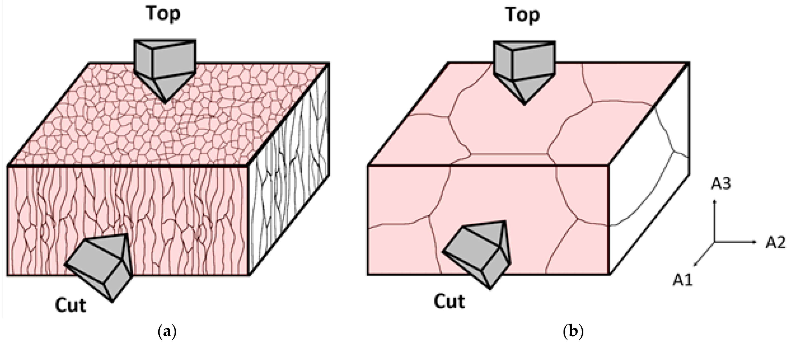
2. Material and Methods

The material chosen for the study was commercially pure nickel (Ni-201) electrolytically plated on the austenitic stainless steel substrate. In pure nickel, plastic deformation is preferentially mediated by dislocation slip, and this material does not show important pile up around the indents (which would complicate the use of the Oliver–Pharr method [11] on load–indentation depth curves).
Nickel plating was performed in a standard industrial coater (Galvanic Engineering Service, Ltd., Sedlnice, Czech Republic) using a nickel sulfamate bath and a current density J of 0.01 and 0.1 A cm−2 to vary the grain size and the preferential crystal growth orientation. The thickness of the deposited layer was about 300 µm.
After electrolytic plating, the sample surfaces were prepared according to the scheme presented in Figure 1 (perpendicular and parallel to the growth direction of the Ni layer) and processed by standard metallographic procedure (mechanical grinding and polishing). The final surface finishing consisted of electrolytic polishing (in 5% perchloric acid solution in ethanol, at 40 V) to remove the surface layer affected by cutting, mechanical grinding, and polishing. One coated sample with [100] fibre texture (see later) was annealed 2 h/1000 °C in air to prepare a coarse-grained reference sample (for the choice of annealing temperature, see e.g., [12,13]). After annealing, the surface was prepared and analysed by the same procedure as for the as-deposited state.
Metallographic analysis was performed for electropolished samples in a scanning electron microscope (SEM) JEOL IT500HR (JEOL Ltd., Tokyo, Japan) equipped with a VelocityTM electron backscatter diffraction (EBSD) camera (EDAX Inc., Warrendale, PA, USA). The samples were inspected at a 70° tilt angle at the positions where nanoindentation tests were performed. The acquired data were evaluated using OIMTM software (version 7.2, EDAX Inc., Mahwah, NJ, USA).
Transmission electron microscopy (TEM) was performed on the samples in the as-deposited state. The samples for TEM were prepared by cutting the surface layer of the substrate with the Ni deposit using a diamond wafering blade. Subsequently, the surface roughness of the deposit was removed using P1200 SiC paper to obtain a plane. The sample was then turned over and the steel substrate was ground to obtain a 100 μm thick platelet (close to the surface of the deposit). Standard TEM 3 mm discs, cut out using Gatan Punch, were ground to a thickness of 40 μm. Thin foils were prepared by twin-jet electrolytic polishing (−32 °C, 20 V) in a Tenupol 5 (Struers, Denmark) device filled with a 6% HClO4 solution in methanol. The microstructural investigation was carried out using a JEOL JEM 2000FX (JEOL Ltd., Japan) transmission electron microscope operated at 200 kV.
Nanoindentation measurements were performed on the NHT2 Nanoindentation Tester (Anton Paar, Neuchâtel, Switzerland) with the Berkovich diamond indenter using the instrumented indentation technique [11]. The tip radius of the Berkovich indenter was about 150 nm (the details about the tip radius estimation methods can be found in [14,15]). The area function was calibrated on fused silica using the standard procedure. The (normal) direction of indentation corresponded to the direction of the Ni growth (orientation top—in axis A3) and perpendicular to the direction of growth (orientation cut—in axis A1). In the top direction, the surface layer of defined thickness was ground off before the indentation so that the measurements were performed at the same location as in the cut direction.
To obtain the mechanical response from different depths, the so-called continuous multicycle (CMC) indentation was used with increasing load, varying the maximum load in each cycle from 0.1 mN to 500 mN. The loading time was 10 s per cycle for CMC, followed by a hold of 5 s at maximum load, and the unloading time was 10 s per cycle. The appropriateness of the method was verified by comparing it with single indentation tests. The hardness H and the contact depth hc were evaluated according to the ISO 14577 standard. At least 10 CMC indentation tests were performed on each sample.

3. Results and Discussion
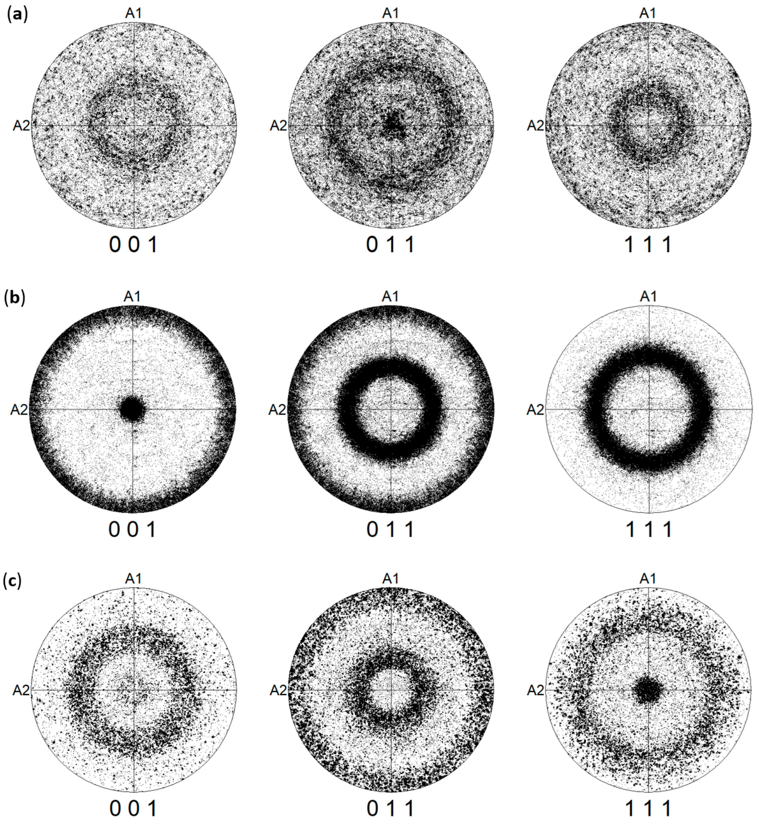
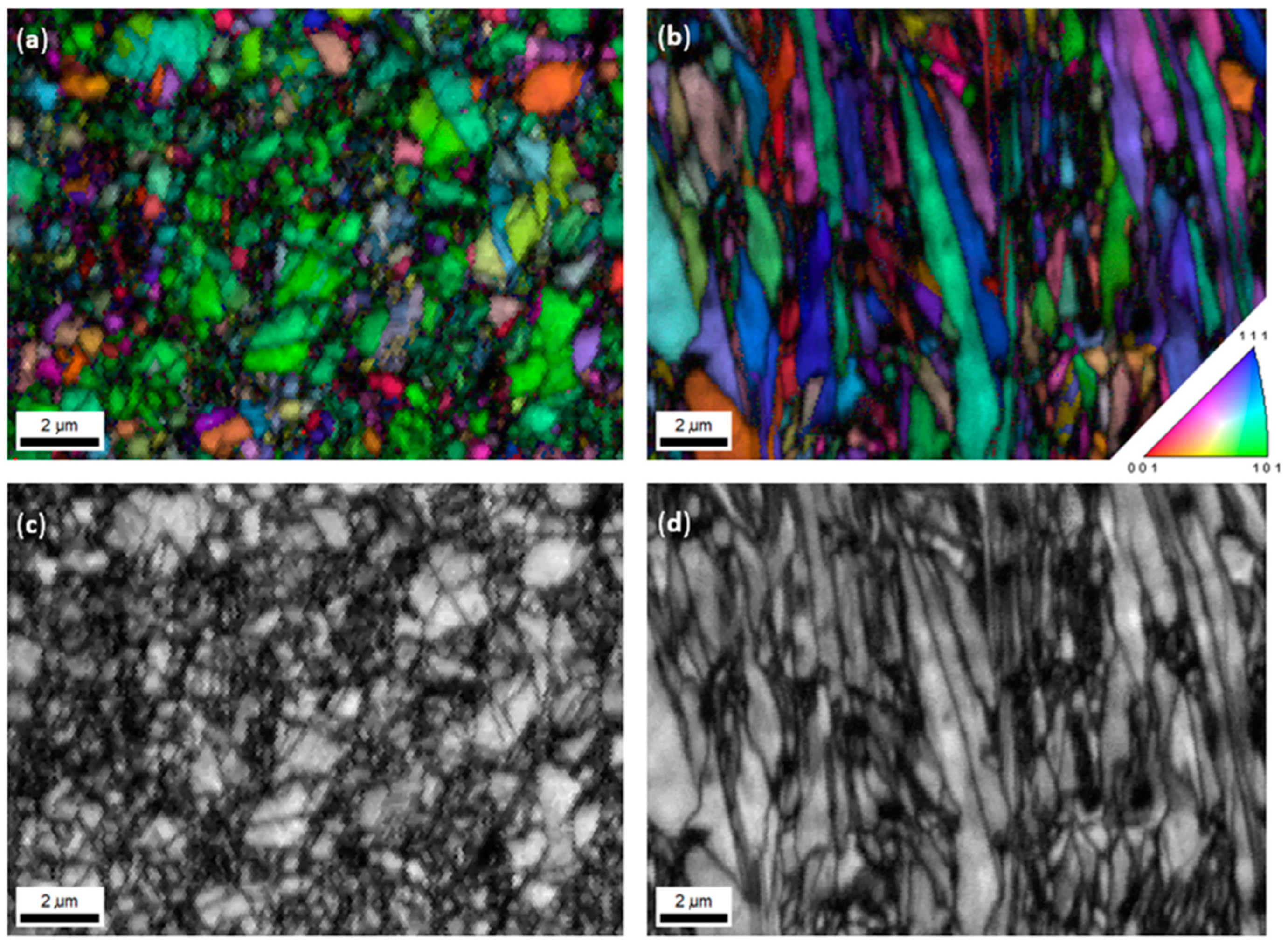
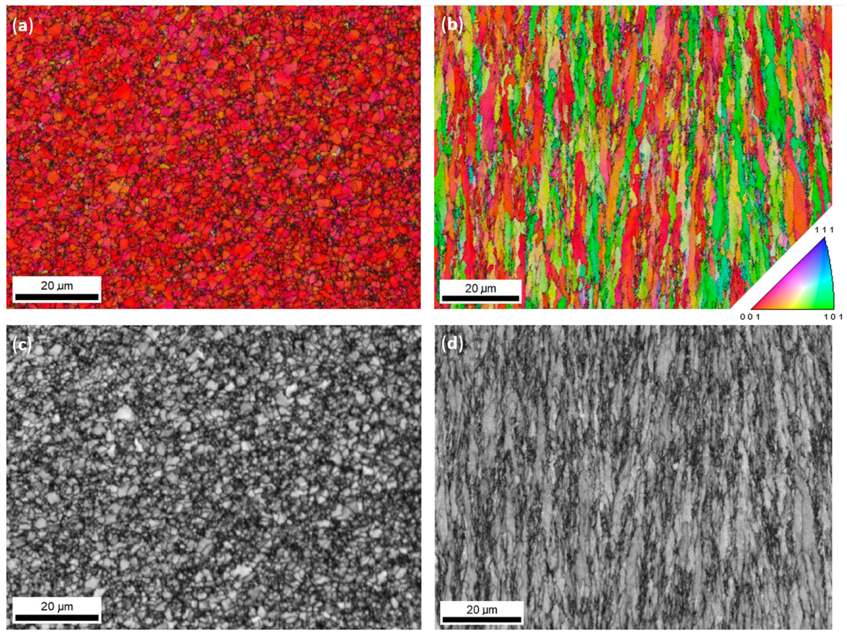
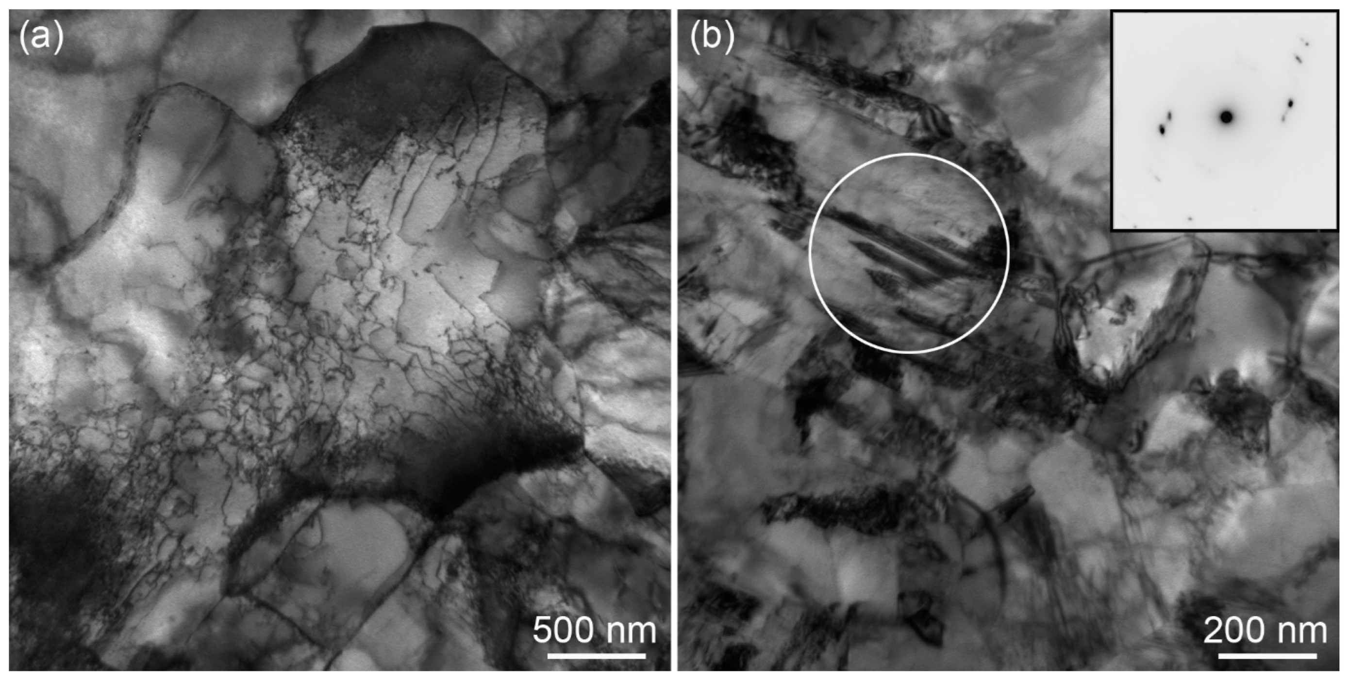
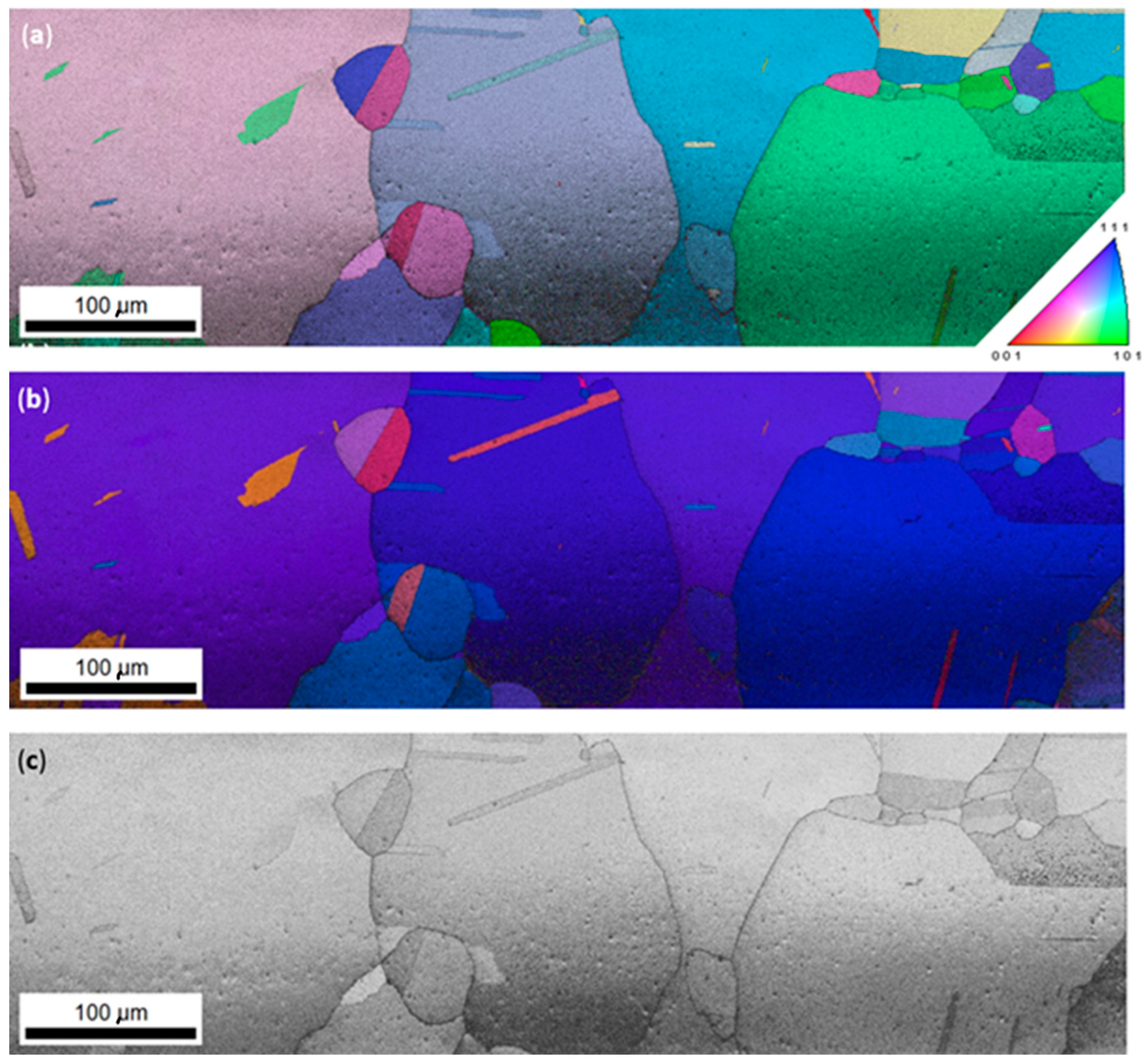
3.1. Microstructure

The grain size and crystal orientation in the electrodeposited layer varied according to the current density. For the lowest current density (0.01 A cm−2), the deposition started with an initial very fine-grained thin layer (thickness less than 20 µm). The grain size was at/below the limit of the EBSD resolution in this layer, so it can be estimated to be less than 100 nm. The crystallographic orientation was “random”; however, as stated before, not all orientations of grains could be identified, especially those of the smaller ones. With increasing distance from the substrate, columnar growth with the [110] fibre texture occurred (see Figure 2a and Figure 3).
The grain sizes ranged from hundreds of nanometres to one or two micrometres perpendicular to the direction of growth and up to approximately ten micrometres in the direction of growth. The average grain/column diameter was evaluated in the cut perpendicular to the direction of growth using EBSD to be 0.66 ± 0.25 µm.
For the current density 0.1 A cm−2, the columnar growth with the [100] fibre texture stabilised very quickly (Figure 2b). The grain sizes ranged from hundreds of nanometres to a few micrometres perpendicular to the direction of growth and to several tens of micrometres in the direction of growth (Figure 4). The average grain/column diameter in the cut perpendicular to the growth direction was evaluated using EBSD to be 1.17 ± 0.22 µm.
These results are in a very good agreement with results of Amblard et al. [16] who found that the grain-oriented growth of Ni coatings changes from [110] to [100] crystal direction, with increasing current density and pointed out that these textures of Ni electrodeposits are attributed to inhibited outgrowth (by hydrogen adsorption) and free-lateral growth, respectively.
TEM observation revealed uneven dislocation substructure (Figure 5a) and numerous nano twins (Figure 5b) in both electrodeposited coatings. Even if nickel has a relatively high stacking fault energy (~120–130 mJ/m2 [17]) which would make it not propitious to form twins, grown-in [18,19] or deformation twins [19] in pure nickel were observed. Some grains contained only a few straight dislocations; in other ones, there were dislocation tangles (Figure 5a). However, the density of dislocations was generally low.
The sample coated with a current density of 0.1 A cm−2 was annealed to prepare a coarse-grained reference sample. After annealing, the grain sizes varied from tens to hundreds of micrometres (some grains grew through the whole thickness of the Ni layer—see Figure 6). The grain size was substantially higher than the size of the indents, so this sample can be considered as a reference (single crystalline). Annealing led to the development of a [111] fibre texture (Figure 2c and Figure 6b).
With respect to these results and according to the scheme of indentation shown in Figure 1, the samples will hereafter be referred to as Ni 111 (annealed) cut/top, Ni 100 cut/top (for layer deposited with the current density of 0.1 A cm−2), Ni 110 cut/top (for layer deposited with the current density of 0.01 A cm−2), and Ni fine grained random (for layer deposited with the current density of 0.01 A cm−2 close to the substrate).

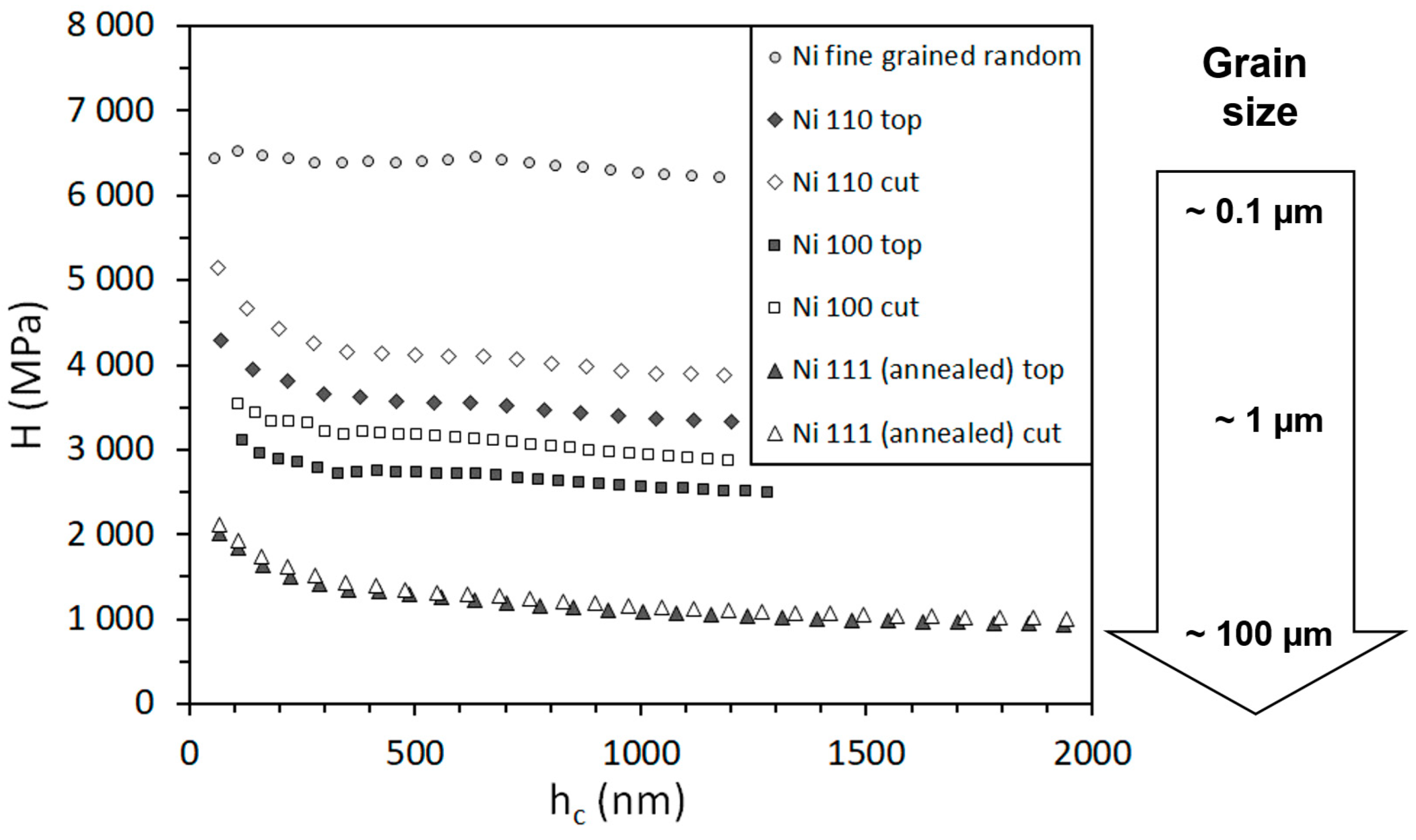
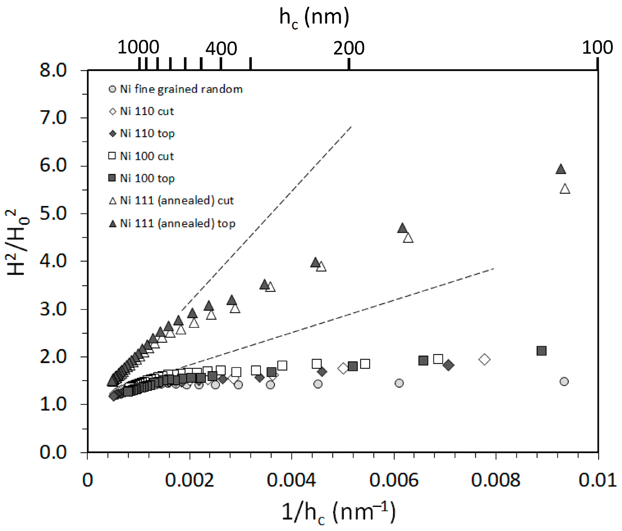
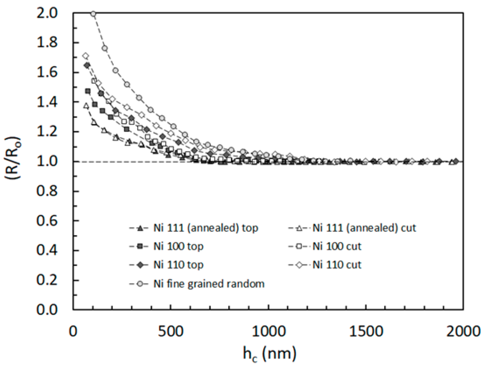
3.2. Nanoindentation

The methodology was first verified by comparing the results of the CMC tests with the results of the single-load indentation tests performed (either at a constant load rate or at a constant strain rate) to different depths. No effect of strain rate, creep during the hold period, or cyclic loading–unloading was observed (as expected); the results of the CMC tests and the single indentations were in very good agreement, confirming the validity of the CMC method.
The evolution of hardness with indentation depth is shown for all characterised samples in Figure 7. Except for the fine-grained, all samples present a significant ISE. In the fine-grained sample, the increase in hardness with decreasing indentation depth is not as pronounced. The hardness increases over all depths with decreasing grain size of the samples. Indeed, the differences in macroscopic hardness (H0) as well as hardness profile cannot be attributed to crystallographic orientation, as the lowest values were obtained in the annealed sample with the [111] fibre texture. The [111] crystal direction is known to be the hardest in nickel; however, the triaxial stress field under the indenter makes the effect of crystallographic orientation on hardness negligible (see e.g., [20,21]). In this case, the lower hardness can certainly be attributed to a larger grain size and a lower dislocation density after annealing.
The hardness measured on the cut is systematically higher than the hardness measured in the top direction, although for annealed (coarse-grained) samples this difference is very small. This increase is therefore probably due to the columnar shape of the grains, which creates a shorter free path for dislocation movement in the cut direction.
The depth dependence of the hardness in the form of normalised H2 vs. 1/h plots is shown in Figure 8. The Nix–Gao model (dashed lines) according to Equation (1) fits the data well for depths higher than around 1 µm, then it deviates. It is also worth noting that after normalisation, the samples with a columnar grain structure show very similar curves regardless of the texture fibre ([100] or [110]) or the indentation direction (top or cut).
On the other hand, the annealed sample, with its coarse grains and lower dislocation density, has a substantially lower hardness H0 and therefore shows distinctly different curves, although very similar in the top or cut indentation directions. Similarly, the fine-grained sample shows a distinctly different curve as it has a substantially higher hardness H0.
To explore this deviation in more detail, we analysed the hardness values at shallow indentation depths using the model considering the limitation of the increase in dislocation density due to the spread out of geometrically necessary dislocations [10].
The modification of the Nix–Gao model developed in previous research [10] consists in the hardness dependence on penetration depth which can be expressed as:
H = H 0 1 + h 0 h 1 e h n h 1
where characteristic depth h1 and shape exponent n are fitting parameters.
As the dependence of hardness on the h/h0 is connected to the density of geometrically necessary dislocations, this equation can be rewritten in the following form:
H = H 0 1 + h 0 h R 0 R 3
where the inverted value of the term in brackets, (R/R0), corresponds to the ratio of effective plastic zone expansion and can be extracted from the experimental results obtained for shallow penetration depth as:
R 0 R h = H 2 H 0 2 1 h h 0 3
The ratio of effective plastic zone expansion is shown in Figure 9. It can be seen that the deviation from the Nix–Gao model becomes larger with decreasing grain size. It is also evident that the deviation from the Nix–Gao model starts earlier with decreasing grain size. This trend is apparent from the identified parameters of the modified Nix–Gao model (Table 1).
In the annealed (coarse-grained) sample, the shape exponent n is around 0.7, which is a value comparable with values obtained for pure metals in previous research [10]. In the same way, the parameter h1 is substantially smaller than the characteristic length h0 from the Nix–Gao model. The deviation from the Nix–Gao model can therefore be attributed to the spread out of geometrically necessary dislocations as the result of the strong repulsive force between them in the constrained volume under the indenter as originally proposed by Swadener et al. [6].
Generally, the most important factor that affects the deviation of the measured hardness from the values predicted by the Nix–Gao model is the lattice friction stress [10]. In the coarse-grained sample, the plastic deformation is realised for both the top and the cut orientations by the same slip systems (with the same lattice friction stress) and cannot be substantially affected by distant grain boundaries.
In samples with columnar grains, the shape exponent n is still in the range 0.7–0.8, but the identified parameters h1 start to approach the characteristic length h0. No effect can be expected from the back-stress induced by existing (statistically stored) dislocations, as the density of dislocations after electrodeposition was very low. In this case, the increase in the effective plastic zone size is probably a consequence of the constraint on the free path for dislocation movement by grain boundaries, resulting in a limited dislocation density inside the grains and a transfer of plastic deformation to adjacent plastically undeformed grains. The spreading of the plastic zone out of the indented single grains caused by the pile up of dislocations was proposed as direct evidence of the activation of new dislocation sources in the neighbouring grains in [22,23].
For the fine-grained sample, the situation is completely different. The deviation from the Nix–Gao model starts earlier (for the depths higher than 1 µm) and is very pronounced. The identified shape parameter n is greater than 1, and the parameter h1 is greater than the characteristic length h0. In other words, although the hardness is very high and for greater indentation depths, it more or less follows the Nix–Gao models, the ISE is very limited at shallow indentation depths. For very shallow indentation depths (<50 nm) and ultrafine grained or nanocrystalline materials, even inverse ISE has been observed in the literature (see e.g., [22,24,25]). However, depths lower than 50 nm were not explored in our paper as the results would inevitably be affected by the change in indenter shape (from pyramidal to rounded) and the onset of plasticity (before first massive pop in).
It is therefore hypothesised that the mechanisms of plastic deformation are different from the previous cases and involve a predominant role of grain boundary-controlled mechanisms such as boundary sliding, grain rotation, and/or grain boundary migration [26]. The change in the deformation mechanism from dislocation-controlled deformation to grain boundary-mediated deformation can make the use of the concept of an extended (effective) plastic zone problematic, and the (modified) Nix–Gao model originally based on geometrically necessary dislocations should be used with care in this case.

4. Conclusions

The breakdown of the Nix–Gao model for indentation size effect at shallow indentation depths was explored in model material with different grain sizes and crystal orientation.
It was confirmed that crystallographic orientation plays a minor role even in deviations from the Nix–Gao model at shallow depths if plastic deformation is already developed under the indenter.
In contrast, decreasing grain size leads to constrained plastic deformation in the grains below the indenter and a progressive deviation from the Nix–Gao model. The evolution of the identified parameters of the modified Nix–Gao model is consistent with the assumed expansion of the plastic zone and the activation of new dislocation sources in adjacent grains.
Further grain refinement down to the nanograin material leads to a probable change in the plastic deformation mechanisms from dislocation-based to grain boundary-mediated deformation and results in an earlier and more pronounced breakdown of the Nix–Gao model for the indentation size effect.

Author Contributions

Conceptualisation, P.H. and B.M.; methodology, P.H. and J.Č.; investigation, P.H., J.Č., J.N. and M.K.; writing—original draft preparation, P.H., J.Č., J.N. and M.K.; writing—review and editing, M.L. and B.M. All authors have read and agreed to the published version of the manuscript.

Funding

This article is based upon work from COST Action CA21121 MecaNano, supported by COST (European Cooperation in Science and Technology–www.cost.eu) and is part of the project Centre of Advanced Applied Sciences (CAAS) No. CZ.02.1.01/0.0/0.0/16_019/0000778 co-financed by the European Union.).

Data Availability Statement

Raw data are available upon reasonable request.

Conflicts of Interest

The authors declare no conflict of interest. The funders had no role in the design of the study; in the collection, analyses, or interpretation of data; in the writing of the manuscript; or in the decision to publish the results.

References

  1. Manika, I.; Maniks, J. Size effects in micro- and nanoscale indentation. Acta Mater. 2006, 54, 2049–2056. [Google Scholar] [CrossRef]
  2. Pharr, G.M.; Herbert, E.G.; Gao, Y. The indentation size effect: A critical examination of experimental observations and mechanistic interpretations. Annu. Rev. Mater. Res. 2010, 40, 271–292. [Google Scholar] [CrossRef]
  3. Nix, W.D.; Gao, H. Indentation size effects in crystalline materials: A law for strain gradient plasticity. J. Mech. Phys. Solids 1998, 46, 411–425. [Google Scholar] [CrossRef]
  4. Durst, K.; Backes, B.; Göken, M. Indentation size effect in metallic materials: Correcting for the size of the plastic zone. Scr. Mater. 2005, 52, 1093–1097. [Google Scholar] [CrossRef]
  5. Huang, Y.; Zhang, F.; Hwang, K.C.; Nix, W.D.; Pharr, G.M.; Feng, G. A model of size effects in nano-indentation. J. Mech. Phys. Solids 2006, 54, 1668–1686. [Google Scholar] [CrossRef]
  6. Swadener, J.G.; George, E.P.; Pharr, G.M. The correlation of the indentation size effect measured with indenters of various shapes. J. Mech. Phys. Solids 2002, 50, 681–694. [Google Scholar] [CrossRef]
  7. Rester, M.; Motz, C.; Pippan, R. Where are the geometrically necessary dislocations accommodating small imprints? J. Mater. Res. 2009, 24, 647–651. [Google Scholar] [CrossRef]
  8. Durst, K.; Backes, B.; Franke, O.; Göken, M. Indentation size effect in metallic materials: Modeling strength from pop-in to macroscopic hardness using geometrically necessary dislocations. Acta Mater. 2006, 54, 2547–2555. [Google Scholar] [CrossRef]
  9. Feng, G.; Nix, W.D. Indentation size effect in MgO. Scr. Mater. 2004, 51, 599–603. [Google Scholar] [CrossRef]
  10. Haušild, P. On the breakdown of the Nix-Gao model for indentation size effect. Philos. Mag. 2021, 101, 420–434. [Google Scholar] [CrossRef]
  11. Oliver, W.C.; Pharr, G.M. An improved technique for determining hardness and elastic modulus using load and displacement sensing indentation experiments. J. Mater. Res. 1992, 7, 1564–1583. [Google Scholar] [CrossRef]
  12. Randle, V.; Rios, P.R.; Hu, Y. Grain growth and twinning in nickel. Scr. Mater. 2008, 58, 130–133. [Google Scholar] [CrossRef]
  13. De Reca, N.W.; Pampillo, C.A. Grain boundary diffusivity via bulk diffusion measurements during grain growth. Scr. Metall. 1975, 9, 1355–1361. [Google Scholar] [CrossRef]
  14. Čech, J.; Haušild, P.; Materna, A.; Kovářík, O. Examination of Berkovich indenter tip bluntness. Mater. Des. 2016, 109, 347–353. [Google Scholar] [CrossRef]
  15. Chicot, D.; N’Jock, M.Y.; Puchi-Cabrera, E.S.; Iost, A.; Staia, M.H.; Louis, G.; Bouscarrat, G.; Aumaitre, R. A contact area function for Berkovich nanoindentation: Application to hardness determination of a TiHfCN thin film. Thin Solid Film. 2014, 558, 259–266. [Google Scholar] [CrossRef]
  16. Amblard, J.; Froment, M.; Maurin, G.; Spyrellis, N.; Trevisan-Souteyrand, E. Nickel electrocrystallization-from nucleation to textures. Electrochim. Acta 1983, 28, 909–915. [Google Scholar] [CrossRef]
  17. Carter, C.B.; Holmes, S.M. The stacking-fault energy of nickel. Philos. Mag. A 1977, 35, 1161–1172. [Google Scholar] [CrossRef]
  18. Vander Voort, G.F. Metallography: Principles and Practice; McGraw-Hill: New York, NY, USA, 1984; ISBN 0070669708. [Google Scholar]
  19. Qiang, J.; Jiang, B.; Dong, Y.; Yang, L.; Drummer, D.; Zhang, L. Tuning residual stress in electrodeposited nickel films via pulse current. Surf. Interfaces 2023, 40, 103038. [Google Scholar] [CrossRef]
  20. Stinville, J.C.; Tromas, C.; Villechaise, P.; Templier, C. Anisotropy changes in hardness and indentation modulus induced by plasma nitriding of 316L polycrystalline stainless steel. Scr. Mater. 2011, 64, 37–40. [Google Scholar] [CrossRef]
  21. Haušild, P.; Materna, A.; Nohava, J. Characterization of anisotropy in hardness and indentation modulus by nanoindentation. Metallogr. Microstruct. Anal. 2014, 3, 5–10. [Google Scholar] [CrossRef]
  22. Yang, B.; Vehoff, H. Dependence of nanohardness upon indentation size and grain size—A local examination of the interaction between dislocations and grain boundaries. Acta Mater. 2007, 55, 849–856. [Google Scholar] [CrossRef]
  23. Jung, B.B.; Lee, H.K.; Park, H.C. Effect of grain size on the indentation hardness for polycrystalline materials by the modified strain gradient theory. Int. J. Solids Struct. 2013, 50, 2719–2724. [Google Scholar] [CrossRef]
  24. Jang, D.; Greer, J.R. Size-induced weakening and grain boundary-assisted deformation in 60 nm grained Ni nanopillars. Scr. Mater. 2011, 64, 77–80. [Google Scholar] [CrossRef]
  25. Ma, X.K.; Chen, Z.; Lu, W.J.; Xiao, L. Continuous multi-cycle nanoindentation behavior of a gradient nanostructured metastable β titanium alloy fabricated by rotationally accelerated shot peening. Mater. Sci. Eng. A 2021, 799, 140370. [Google Scholar] [CrossRef]
  26. Yu, Q.; Legros, M.; Minor, A.M. In situ TEM nanomechanics. MRS Bull. 2015, 40, 62–70. [Google Scholar] [CrossRef]
Figure 1. Sample coordinate system and indentation scheme in the electrodeposited layer (a), and after grain coarsening (b). The directions of indentation are denoted Top and Cut.
Crystals 13 01385 g001
Figure 2. Summary of pole figures in nickel layers obtained by electrodeposition with a current density of 0.01 A cm−2 (a), a current density of 0.1 A cm−2 (b), and after electrodeposition with a current density of 0.1 A cm−2 and annealing 2 h/1000 °C (c). The direction of growth corresponds to the A3 (normal) axis. Clearly developed [110], [100], and [111] fibres can be observed.
Crystals 13 01385 g002
Figure 3. EBSD maps of electrodeposited Ni layer obtained with a current density of 0.01 A cm−2. Image quality maps (visualisation of microstructure) with superimposed inverse pole figures showing the crystallographic orientation on the top (a) and in the cut (b) of the sample. Morphology of grains (depicted using image quality maps) on the top (c), and in the cut (d) in the same position.
Crystals 13 01385 g003
Figure 4. EBSD maps of Ni layer obtained by electrodeposition with a current density of 0.1 A cm−2. Image quality maps with superimposed inverse pole figures showing the crystallographic orientation on the top (a), and in the cut (b) of the sample. Visualisation of microstructure (using image quality maps) on the top (c), and in the cut (d) in the same position. Note the columnar growth and a distinctive [100] fibre texture.
Crystals 13 01385 g004
Figure 5. Bright-field TEM micrographs of the fine microstructure of the nickel layer electrolytically deposited with a current density of 0.1 A cm−2: (a) Dislocation substructure, (b) Very small grains and grown-in nano twins (the circle shows the size and position of the selective area aperture, the diffraction pattern with twin double diffraction spots is in the inset).
Crystals 13 01385 g005
Figure 6. EBSD maps showing the microstructure in the Ni layer after annealing 2 h/1000 °C. Image quality maps with superimposed inverse pole figure showing distribution of the crystallographic orientation in the cut direction—in axis A1 (a), and in the direction perpendicular to the surface—in axis A3 (b)—clear [111] fibre texture in the top orientation can be seen. Image quality map showing the coarse-grained microstructure (c).
Crystals 13 01385 g006
Figure 7. Hardness as a function of contact depth for Ni electrodeposited layers with different grain size and crystallographic orientation.
Crystals 13 01385 g007
Figure 8. Normalised Nix–Gao plot (H2 vs. 1/hc) showing the deviation from the Nix–Gao model (dashed lines) fitted for greater depths.
Crystals 13 01385 g008
Figure 9. Increase in effective plastic zone size for shallow indentation depths. Note that the deviation from the Nix–Gao model (R/R0 = 1) becomes larger with decreasing grain size.
Crystals 13 01385 g009
Table 1. Parameters of the modified Nix–Gao model identified on samples with different grain size (obtained with different current densities).
J (A cm−2)D (nm)H0 (MPa)h0 (nm)h1 (nm)n
Ni 111 (annealed) top0.1~1057521077370.68
Ni 111 (annealed) cut0.1 818990370.68
Ni 100 top0.1~1032205356850.78
Ni 100 cut0.1 24614271450.73
Ni 110 top0.01~50029223681280.80
Ni 110 cut0.01 33434361100.75
Ni fine grained random0.01~100536340822601.20
Disclaimer/Publisher’s Note: The statements, opinions and data contained in all publications are solely those of the individual author(s) and contributor(s) and not of MDPI and/or the editor(s). MDPI and/or the editor(s) disclaim responsibility for any injury to people or property resulting from any ideas, methods, instructions or products referred to in the content.

