Article

Research on Crystal Structure Evolution and Failure Mechanism during TSV-Metal Line Electromigration Process

1
School of Material Science and Engineering, Xiamen University of Technology, Xiamen 361024, China
2
Science and Technology on Reliability Physics and Application of Electronic Component Laboratory, The 5th Electronics Research Institute of the Ministry of Industry and Information Technology, Guangzhou 511370, China
*
Authors to whom correspondence should be addressed.
Crystals 2024, 14(1), 37; https://doi.org/10.3390/cryst14010037
Submission received: 14 November 2023 / Revised: 19 December 2023 / Accepted: 22 December 2023 / Published: 27 December 2023
(This article belongs to the Section Inorganic Crystalline Materials)

Abstract

:
The combined use of Through Silicon Via (TSV) and metal lines, referred to as TSV-metal lines, is an essential structure in three-dimensional integrated circuits. In-depth research into the electromigration failure mechanism of TSV and the microstructure evolution can serve as theoretical guidance for optimizing three-dimensional stacking. This article conducted electromigration experiments on TSV-metal line structural samples at current densities of 1.0 × 10⁵ A/cm2, 5 × 10⁵ A/cm2, and 1 × 10⁶ A/cm2. Additionally, Electron Back Scattered Diffraction (EBSD) technology was employed to systematically investigate the microstructural evolution of the TSV-metal line structure profiles before and after the application of electrical testing. The results indicate that the current induces a change in the crystal orientation at the TSV-metal interface (TSV/metal interface) and the bottom metal line. This phenomenon notably depends on the initial angle between the grain orientation and the current flow direction. When the angle between the current direction and the grain orientations [001] and [010] is relatively large, the crystals are more likely to deviate in the direction where the angle between the grain orientation and the current is smaller. This is because, at this point, the current direction is precisely perpendicular to the <100> crystal plane family, where the atomic density is lowest, and the energy required for electron transport is minimal. Therefore, the current readily rotates in the direction of this crystal orientation. Before the electromigration tests, areas with a high level of misorientation were primarily concentrated at the TSV/metal interface and the corners of the TSV-metal line. However, these areas were found to be more prone to developing voids after the tests. It is conjectured that the high misorientation level leads to elevated stress gradients, which are the primary cause of cracking failures in the TSV-metal line. As the current density increases from 5 × 10⁵ A/cm2 to 1 × 10⁶ A/cm2, the electromigration failure phenomena in the TSV become even more severe.

1. Introduction

The Through Silicon Via (TSV) technology utilizes the shortest vertical interconnections to establish electrical connections between chips, significantly enhancing the data transfer speed and packaging density between chips. It is a core technology in 3D packaging and provides a viable pathway for 3D integration [1,2,3,4,5,6]. In recent years, with the continuous increase in chip interconnect density, research on the reliability issues of TSV-metal lines has also deepened. Among these issues, thermal stress, thermal migration, and electromigration are key factors that have made TSV reliability problems increasingly severe [7,8,9]. During the TSV electromigration process, changes in material microstructure and temperature can lead to the accumulation of vacancies, which, in turn, can give rise to voids. The formation and growth of voids result in an increase in resistance at the interconnect location and may ultimately lead to open circuits, causing electromigration failures. To gain a deeper understanding and enhance the reliability of TSV interconnect structures, researchers employ various methods to conduct failure analysis, simulate calculations, and investigate microscale mechanisms of TSV electromigration.
Ma Rui et al. [10] established a three-dimensional finite element model of TSV interconnect structures and conducted electro-thermal coupled analysis. Their research findings indicate that, within a certain range, current density and ambient temperature are the primary factors influencing the electromigration lifetime of TSV interconnect structures. This provides important insights for understanding and optimizing the electromigration performance of TSV interconnect structures. Chen et al. [11] investigated the failure locations of TSV electromigration and used finite element methods to predict the failure locations of individual TSVs. This approach provides a robust tool for identifying potential failure points. Gousseau et al. [12] conducted research using electron backscattered diffraction and in situ scanning electron microscopy to investigate the impact of the microstructure of TSV-Cu on the formation and growth of electromigration-induced voids. Chen Zhaohui [13], through the establishment of an electromigration simulation model, conducted a comprehensive and systematic study on the reliability of silicon TSV electromigration. By conducting accelerated experiments, detailed data on factors such as current density and temperature gradients were obtained, along with calculations for relative atomic concentration distribution. The results reveal that silicon TSV electromigration issues primarily occur at the connection points between the solder pad and copper pillar, or in the vicinity of the edges of the former. Further research suggests that this is mainly caused by stress gradients triggering atomic migration. Jiwoo Pak et al. [14] conducted research focused on the electromigration reliability of silicon through-silicon vias (TSVs) and carried out electromigration lifetime simulation studies. They discovered that the stress intensity provided by TSVs has a certain influence on the electromigration process, resulting in an impact on the lifetime of nearby interconnects. Thomas Frank et al. [15] conducted a study on the electromigration characteristics of TSVs within three-dimensional integrated circuits, analyzing the impact of TSV dimensions on electromigration lifetime and metal thickness. The research findings indicate that the metal interface position of TSV directly affects electromigration performance, while metal thickness does not have any influence on the electromigration process. W. H. Zisser et al. [16] conducted an in-depth study on the electromigration reliability of silicon TSVs through multiple sets of simulation experiments. They investigated the stress distribution and evolution within TSV structures without voids and examined the positioning patterns of void formation. Furthermore, they introduced voids into the original structures to enhance impedance effects and tracked the subsequent evolution of voids. The research results demonstrate that impedance exhibits non-linear dynamic changes over time, primarily due to the occurrence of open circuit failures. The study also focused on analyzing the influence of different current densities, highlighting the high adaptability of the Shockley equation. Marco Rovitto et al. [17] conducted research on the electromigration failure time issue of silicon TSVs using the Shockley equation. Leveraging conditional parameters, they successfully established a model for electromigration void nucleation. By combining this model with the equation, they found that when conditional parameters vary, the final results closely align with the Shockley equation. Ni Hao [18] conducted research on finite element simulation techniques and failure mechanisms of TSV structures under three different single stress fields: electrical, thermal, and vibrational. He performed qualitative analysis of the simulation results based on failure physics and made lifetime predictions using a failure physics model.
Many of the studies mentioned above are heavily based on the data from accelerated TSV electromigration tests for reliability research or the fitting of their failure physics models. However, even with the same TSV-metal liner structural parameters, notable differences in electromigration behavior can be observed when different fabrication processes are used. The impact of the microstructure of the TSV-metal liner on its failure should not be underestimated.
In this paper, a study on the electromigration failure mechanisms of TSV-metal lines under different electrical stresses is conducted. Firstly, electromigration tests were performed under an electrical stress of 1.0 × 10⁵ A/cm2, and the impact of the current on the Cu grain orientation in the TSV-metal line is discussed. Subsequently, electromigration tests were conducted under electrical stresses of 5 × 10⁵ A/cm2 and 1 × 10⁶ A/cm2. By comparing the differences in crystal orientation and grain boundary misorientation of the TSV-metal line before and after electromigration, the formation mechanism of voids during the electromigration process is discussed.

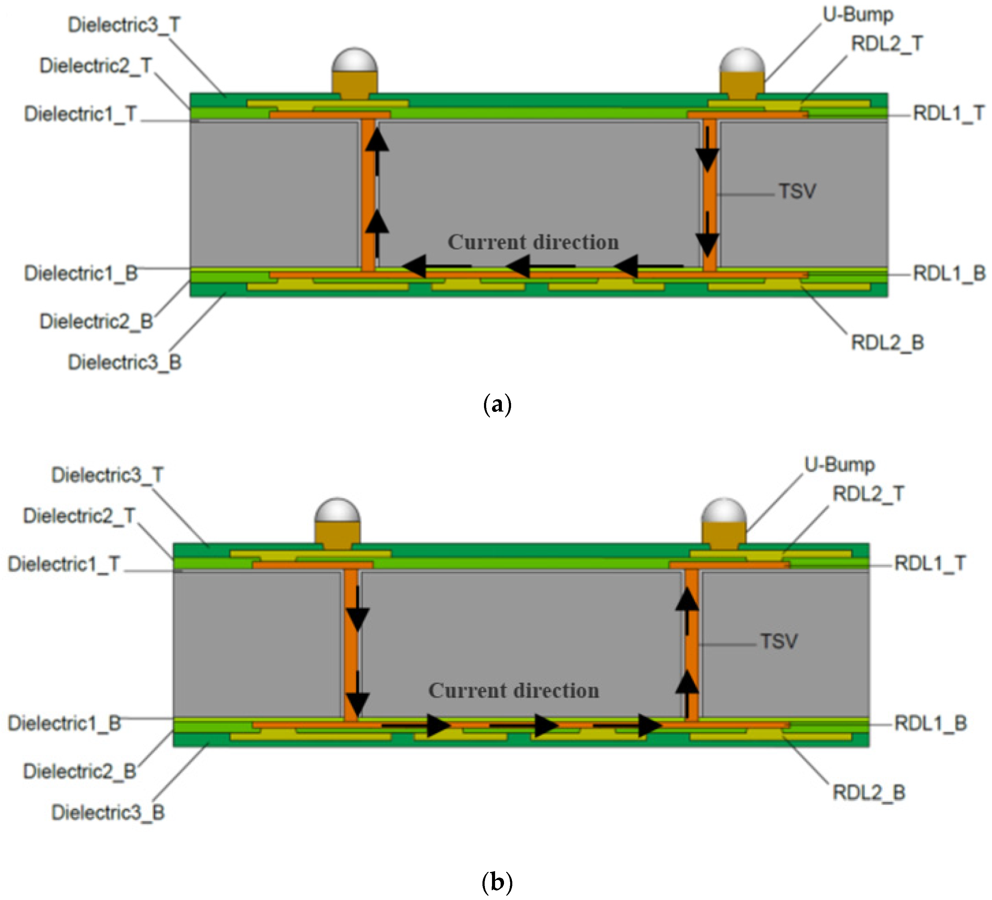
2. TSV Electromigration Experiment
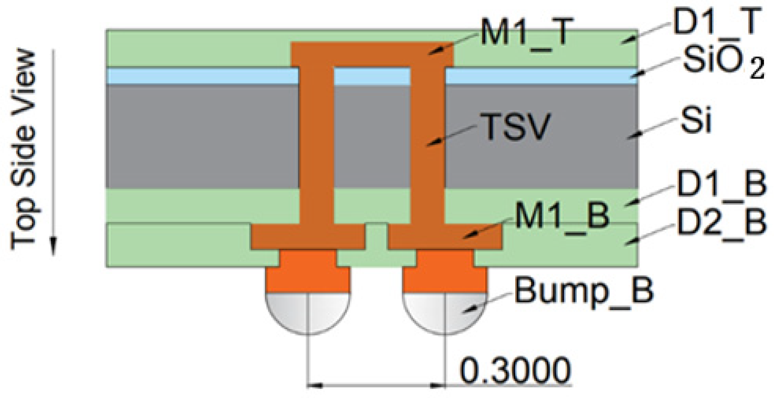
2.1. Test Samples

The sample structure of the TSV-metal line with a diameter of 20 μm and a thickness of 100 μm used for the experiment is shown in Figure 1, and the specific dimensional values of the cross-section are provided in Table 1. The cross-sectional diagram of the TSV sample, from top to bottom, consists of D1_T (photoresist insulating layer), M1_T (redistribution layer), silicon dioxide layer, TSV and silicon layer, D1_B and D2_B (photoresist insulating layers), M1_B (redistribution layer), and bumps. Electrical migration tests were conducted by applying current load to two bumps on the sample surface. The specific test conditions for the four cases are outlined in Table 2, and the current direction is illustrated in Figure 2.

2.2. Electromigration Test Platform

The electromigration experiments were conducted using the Lake Shore CRX-6.5K probe station, as shown in the experimental setup in Figure 3a. This setup includes a cooling compressor, temperature controller, LCD display, illumination lamp, vacuum pump assembly, ultra-low-temperature four-point probe station (Figure 3b), cooling circulation water system, and a DC current source.
The cooling compressor is used to lower the temperature inside the probe station chamber, while the temperature controller is employed to regulate the temperature of the sample stage inside the chamber. Their combined use ensures the desired test temperature for the samples.

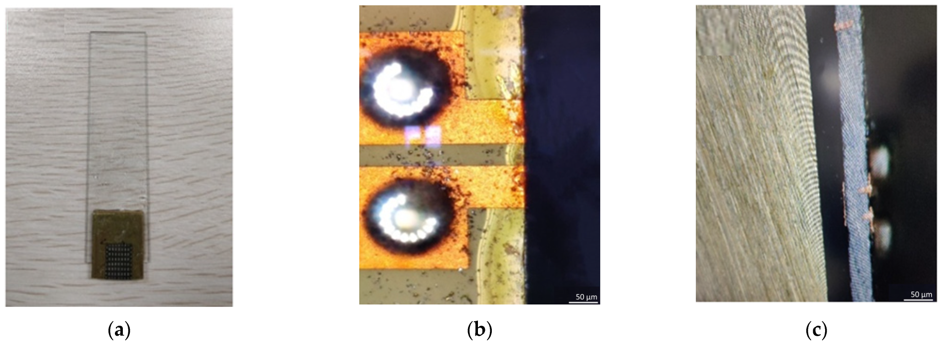
2.3. Microstructure Analysis

The microstructure of the TSV-metal line sample profile was analyzed before and after electromigration experiments. First, the slides, copper sheets, and TSV-metal line samples were bonded together using hot melt adhesive on a heating table, the overall size of the samples was 1 × 1 cm for the bare chips, and the specimens after bonding are shown in Figure 4a. Then, the MP-2B metallographic grinder (Shanghai Metallographic Machinery Equipment Co., Ltd., Shanghai, China) was used to grind the profile of the bonded TSV-metal line sample, and the VHX-7000 metallographic microscope (VHX-7000 Metallographic Microscope–Keyence, Osaka, Japan) was used to observe the grinding cross-section until the grinding was close to the edge position of the TSV. Figure 4b,c show the surface morphology and cross-section morphology of the milled samples, respectively. The cross sections of the samples after the electromigration experiments were trimmed by FIB using a Helios G4 CX Focused Ion Beam (FIB) (Helios G4 CX Focused Ion Beam–Thermo Scientific, Brno, Czech Republic) at 30 KV/9.3 nA, and then the cross sections of the samples after the electromigration experiments were trimmed by an Oxford Instruments Symmetry EBSD system (Electron Backscattered Diffraction), an FEI Symmetry EBSD system (Electronic Backscattered Battery Diffraction), and an FEI Helios G3 CX Scanning Electron Microscopy (SEM) (FEI Helios G3 CX Scanning Electron Microscope–FEI, Omaha, NE, USA) to obtain microstructural information of the TSV-metal line profile.

3. Results Discussion and Analysis

3.1. Effect of Cu Crystal Orientation on TSV-Metal Liner Electromigration

Figure 5a–d show SEM images of various locations on sample A before electromigration. The sample was subjected to a current of 0.159 A (current density of 105 A/cm2) at 100 °C for 210 h, with the current flowing in from the right-side anode and out from the left-side cathode. Figure 6a–d display SEM images of sample A after the electromigration test. Upon comparing Figure 5 and Figure 6, it can be observed that there is no significant damage or void formation in the TSV-metal line structure profile before and after the electromigration test.
In order to further analyze the effect of electromigration on the microstructural evolution of the TSV-metal line, the TSV-metal line profile was analyzed by EBSD in conjunction with the positional relationship of the crystal orientation coordinate system with respect to the sample coordinate system [19,20,21,22,23]. The sample coordinate axis in this study is plotted against the TSV sample and the orientation of the current in the test in Figure 7.
Considering that the three crystal axes of the sample crystals have no obvious characteristic differences, in order to facilitate the numerical calculation, the angle between the orientation direction of the sample crystal [001] and the electric current is specified as θ. The HKL Channel 5 software is used to obtain the three Euler angles (Φ, φ1, φ2) of the grains of the upper cathodes No. 1–10 in the TSV-metal line, and then the angle between the orientation direction of the upper cathode crystal [001] and the coordinate axis ND in the sample cathode is calculated in the direction of ND. The angle between the orientation direction of the upper cathode crystal [001] and the coordinate axis ND is calculated in the ND direction, combined with the fact that the current direction is the same as that of ND in Figure 7, so the angle between the orientation direction of the upper cathode crystal [001] and the coordinate axis ND is the angle θ between the orientation direction of the sample crystal [001] and the current direction; similarly, in the TD direction, the angle between the orientation direction of the sample crystal [010] and the coordinate axis TD is calculated, and this is the angle θ between the orientation direction of the sample crystal [010] and the current direction [24,25,26].
The microstructural evolution of the top and bottom regions of the TSV-metal line before and after electromigration is shown in Figure 8 and Figure 9.
Comparison of the top of the anode before and after electromigration (Figure 9) reveals that the angle between grain orientation [010] and current direction decreases by 2.3° and 3.1° for grains 1–2 in the left corner, and the angle between grain orientation [001] and current direction decreases by 1.1°,1.2°,0.6°,1.6°, and 1.3° for grains 3–7 in the middle region.
The angle between the current flow direction of the anode upper 3–7 grains and the grain [001] orientation is larger, crystal orientation of the 3–7 grains and the angle between the current are shown to decrease after the test. The change rule between current direction and grain [010] orientation is the same as the former. For example, in the upper part of the anode (Figure 9a), the direction of the current of grains 1–2 has a large angle with the grain [010] orientation axis, and from the above it can be seen that the angle of their currents with respect to the orientation presents a decrease after the test. In fact, this current direction correlation of grain orientation deflection has been reported in a large number of studies [27,28,29,30,31], and grain orientation is one of the key factors dominating the electromigration behavior during the electromigration process.
During TSV electromigration, the current induces a change in crystal orientation at the top of the TSV-metal line and at the bottom of the metal line. The phenomenon of grain orientation change during electromigration significantly depends on the angle between grain orientation and current flow direction in the initial state. Thus, it can be concluded that when the angle between the current direction and grain orientation [001] and grain orientation [010] is large, the crystal is more likely to be deflected in the direction where the angle between the grain orientation and the current decreases. This is due to the fact that this current direction is exactly perpendicular to the <100> crystal plane family, where the atomic concentration is the sparsest and the jump energy required for electron gas propagation is lowest. As a result, the crystal is prone to crystallographic deflection in that direction.
In grains 1–10 in Figure 8a, the degree of change in the angle between orientation and current after the test is overall greater than that of grains 1–9 in Figure 9a, presumably due to the greater electronic wind force on the grains at the upper TSV-metal line of the cathode relative to that at the anode. In addition, overall, the region with the largest grain orientation shift is located in the region near the lower TSV-metal line at the anode.

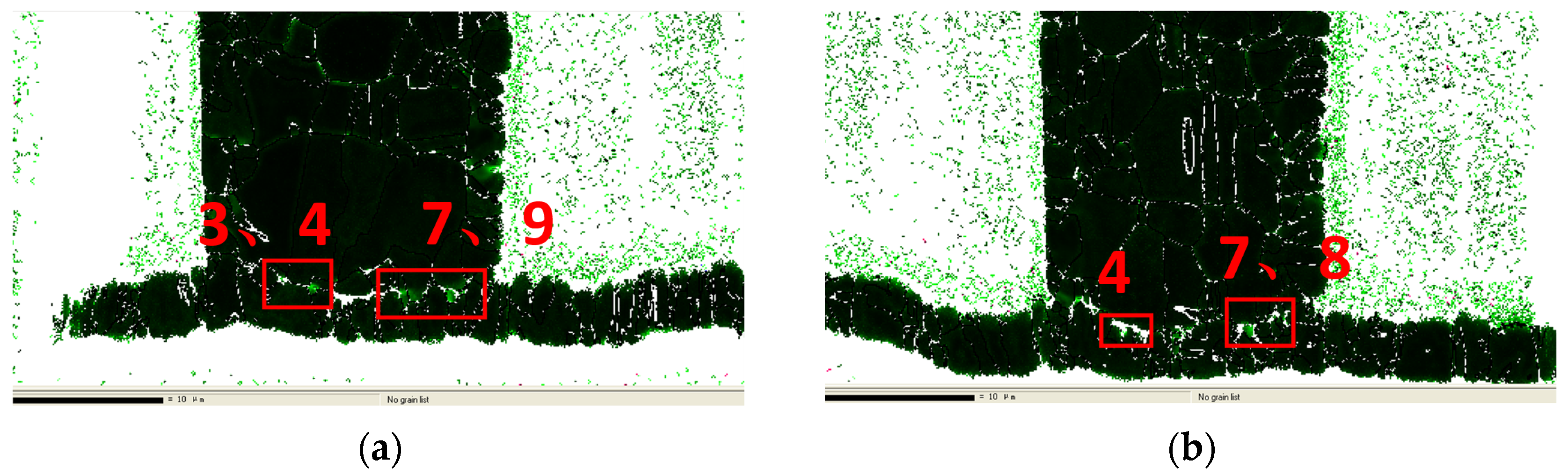
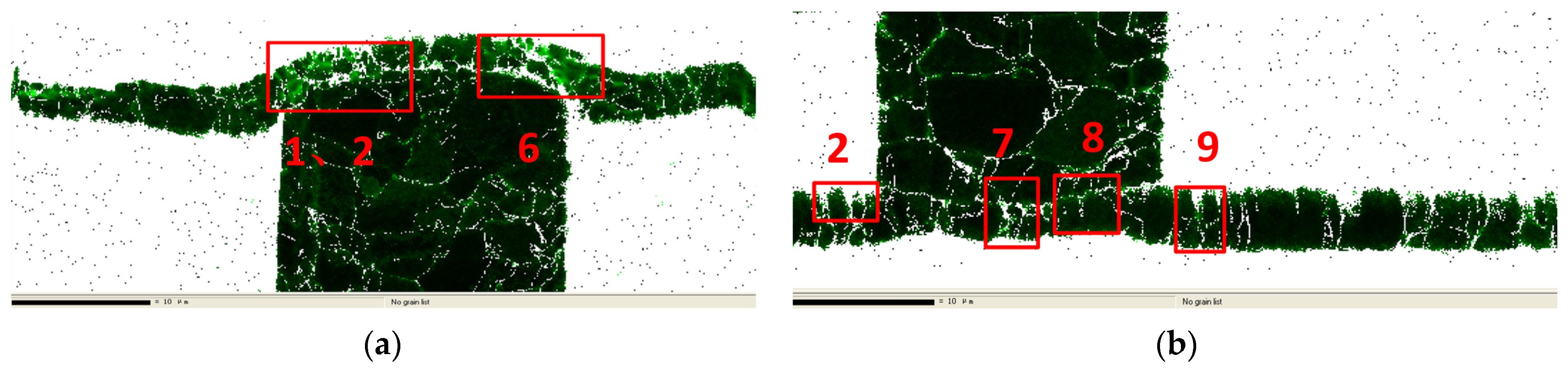
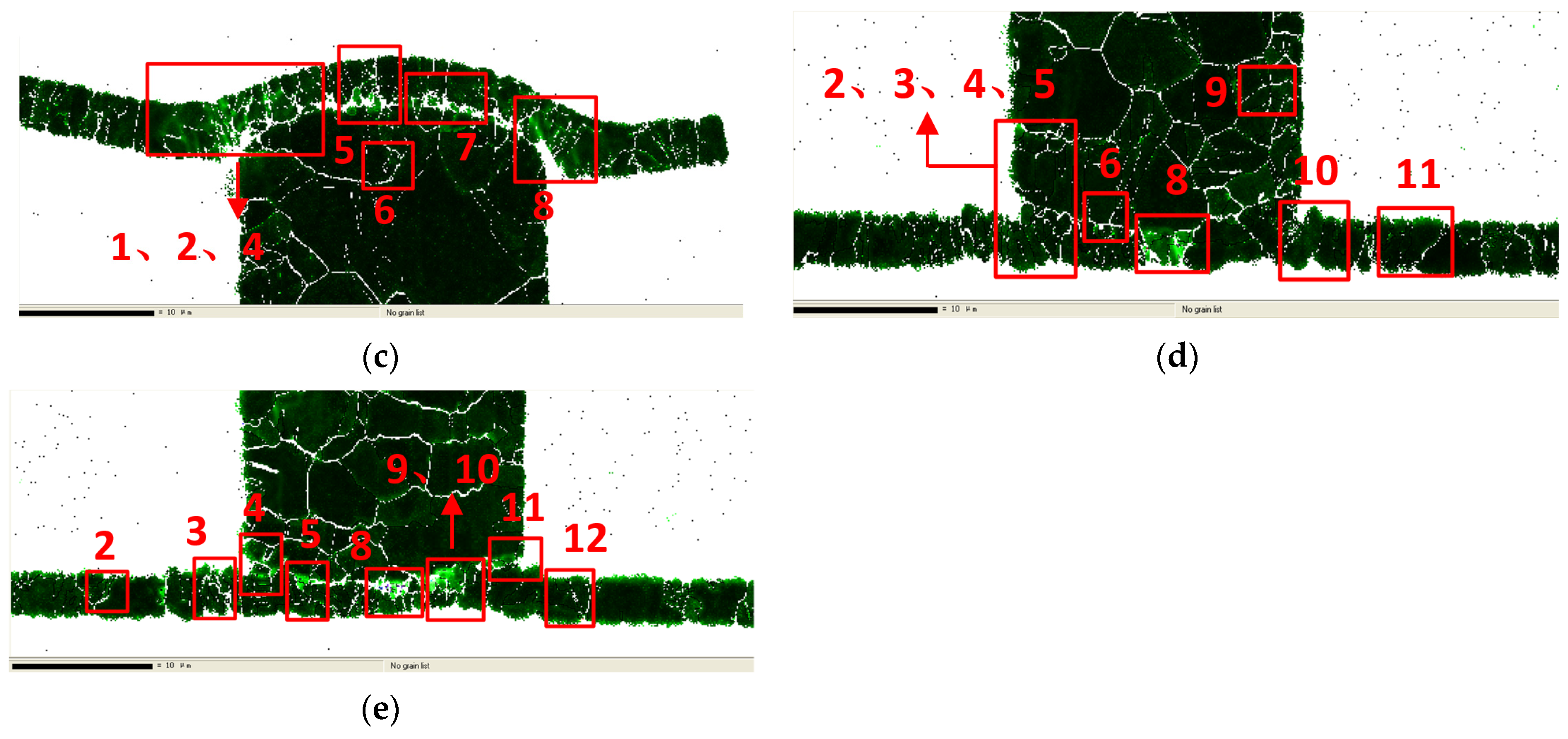
3.2. The Influence of Inter-Grain Misorientation on TSV-Metal Line Electromigration

3.2.1. Conditions of 5 × 10⁵ A/cm2 Current Density

Figure 10 and Figure 11 depict SEM images of the lower parts of the TSVs under the cathode and anode, respectively, before and after electromigration. From Figure 10a and Figure 11a, it is evident that the surfaces of the lower parts of the TSVs under both the cathode and anode in sample B were smooth and defect-free before the experiment. After the experiment, holes formed at the TSV-metal line locations under the cathode (Figure 10b) and anode (Figure 11b), with noticeable expansion of gaps. Relevant studies suggest that interfacial diffusion of atoms is the primary mechanism for Cu interconnect electromigration, and this interfacial diffusion easily leads to the formation of voids at interfaces. Voids, in turn, experience surface diffusion, accelerating the formation of voids [32].
Misorientation is a key parameter to measure the internal micro-strains in the material [33,34,35] and can be used to study the internal micro-strains in the TSV before and after the test. As shown in Figure 12a,b, the EBSD plots of the lower part of the cathode and anode before the test are shown, respectively, while Figure 12c,d show the EBSD plots of the lower part of the cathode and anode after the test.
The magnitude of grain boundary misorientation at positions 1–10 in Figure 12a,b is shown in Table 3 below.
According to Figure 10 and Figure 11, it can be observed that the lower surfaces of both the TSV cathode and anode were smooth and defect-free before the experiment. After the experiment, perforations in the form of holes were present in the TSV-metal lines in the lower parts of both the cathode and anode. However, the number of holes formed in the lower part of the anode was relatively less, and the gaps in its TSV-metal lines noticeably widened. Following the experiment, Figure 12a transformed into the configuration depicted in Figure 12c. Combining SEM images Figure 10b–d, it is evident that positions 3, 4, 7, and 9 in Figure 12a correspond to the regions where holes formed after the experiment.
After the experiment, the lower part of the anode TSV is illustrated in Figure 12d, and combining SEM images Figure 11b–e reveals that holes formed after the experiment at positions 4, 7, and 8 in Figure 12b.
It can be observed that positions with significant misorientation in the crystal grain boundaries are 3, 4, 7, and 9 in Figure 12a, with misorientation angles of 59.88°, 59.96°, 55.59°, and 59.61°, respectively. In Figure 12b, positions with notable misorientation are 4, 7, and 8, with misorientation angles of 59.96°, 51.66°, and 59.94°, respectively.
The occurrence of holes exhibits a strong dependence on misorientation intensity. Positions 3, 4, 7, and 9 in Figure 12a have significant misorientation, making them the main locations for hole formation. Similarly, positions 4, 7, and 8 in Figure 12b exhibit notable misorientation, designating them as the primary sites for hole formation [33,34,35].
The misorientation cloud map of the lower section of the TSV cross-section before electromigration is depicted in Figure 13. Bright regions in the misorientation cloud map typically signify areas with a high level of misorientation. In Figure 13a, positions 3, 4, 7, and 9, and in Figure 13b, position 4, 7, and 8 all correspond to areas with a high level of misorientation. Combining this information with Figure 10 and Figure 11, it is evident that these positions coincide with the locations where holes form. Moreover, angle data indicate that the misorientation values at hole formation locations are generally higher than in other regions. Therefore, it can be inferred that regions with a high level of misorientation are prone to hole formation or defects after electromigration.

3.2.2. Conditions of 1 × 10⁶ A/cm2 Current Density

SEM images of sample C before and after electromigration are presented in Figure 14. In Figure 14a,c, the TSV-metal liner cathode profile is dense, and the TSV-metal interface is well-bonded before electromigration. After electromigration, significant holes appear at the TSV-metal interface and within the metal liner, as indicated in Figure 14a,c. To elucidate the pattern of hole formation more precisely, electron backscatter diffraction (EBSD) observations were conducted on the cathode TSV-metal line of sample C before and after electromigration, as shown in Figure 15. Table 4 displays the misorientation values of grain boundaries at positions 1, 2, and 6 in Figure 15a,c. Among them, the misorientation values between grains at positions 1, 2, and 6 in Figure 15a are relatively high. After electromigration, the upper EBSD image in Figure 15b corresponds to positions 1, 2, and 6 in Figure 15a. Combining this with the SEM image in Figure 14b, it is evident that holes form at positions 1, 2, and 6 after the experiment. In Figure 15c, the misorientation values at positions 2, 7, 8, and 9 are relatively high. In the lower part of the cathode, before and after electromigration (Figure 15c,d), holes also form in regions with high misorientation levels. Combining this with SEM image 14d, it is observable that after the experiment, holes of varying sizes form at positions 2, 7, 8, and 9.
In contrast to sample C, sample D has the anode on the left side and the cathode on the right side of the TSV. Figure 16 illustrates SEM images of various regions of sample D before and after the experiment. The results reveal that there were some holes present in the upper part of the anode TSV before the experiment (Figure 16a), which is related to the fabrication process of the sample. After the experiment, a significant number of holes formed in this area (Figure 16b). In the lower part of the anode TSV, holes formed at the TSV-metal line locations (Figure 16d). However, compared to the lower part of the cathode TSV (Figure 16f), the degree of electromigration was somewhat mitigated, likely due to the greater electron wind force on the cathode. The surface of the cathode TSV lower part had no apparent defects before the experiment (Figure 16e), but numerous holes formed at the TSV-metal line locations after the experiment (Figure 16f). Although the current flow was consistent in the cathode TSV lower parts of both samples C and D, the locations of hole formation differed. This suggests that different TSV grains may be affected differently by the electric current.
Figure 17 displays EBSD images of various cross-sectional locations of sample D before and after electromigration, with the misorientation of grain boundaries at positions Figure 17a,c,e provided in Table 5.
Examining the misorientation data in Figure 17a and correlating it with the SEM image in Figure 16b, it is evident that holes formed at positions 1, 2, 4, 5, 6, 7, and 8 after the experiment. Notably, the misorientation values at these positions are relatively higher compared to other locations. Figure 17b illustrates the grain morphology after the formation of holes at positions 1, 2, 4, 5, 6, 7, and 8.
Similarly, by combining the misorientation data in Figure 17c and the SEM image in Figure 16d, it is observed that positions 2, 3, 4, 5, 6, 8, 9, 10, and 11, where the misorientation values are relatively high, exhibit hole formation after the experiment. Figure 17e,f respectively depict EBSD images of the lower part of the cathode TSV in sample D before and after the experiment. Analyzing the misorientation data in Figure 17e and the SEM image in Figure 16f reveals that holes formed after the experiment at positions 2, 3, 4, 5, 8, 9, 10, 11, and 12, with the morphology of the formed holes indicated in Figure 17f. Similar to sample C, the hole formation locations in sample D are consistently in regions with higher misorientation values, particularly around the TSV-metal line and its corners, with the upper part of the anode TSV experiencing the most severe failures.
By utilizing Channel 5 software, misorientation cloud maps were further extracted separately for the pre-electromigration conditions in Figure 15a,c and Figure 17a,c,e, as depicted in Figure 18. In Figure 18a, it is observed that the upper part of the cathode TSV-metal line in sample C before the electromigration experiment appears as a bright region, indicating a high level of misorientation in this area. Furthermore, based on Figure 15a, it is evident that specific misorientation values at the grain boundaries, particularly at positions 1, 2, and 6 in Figure 18a, are relatively higher than at other locations. As previously indicated by Figure 14b and Figure 15b, the regions where holes formed after the experiment in sample C are located within positions 1, 2, and 6 in Figure 18a. This reflects that holes are prone to form in areas with higher misorientation levels, specifically in proximity to regions with larger misorientation values at the grain boundaries.
Figure 18b illustrates the misorientation cloud map of the lower part of the cathode TSV in sample C before the electromigration experiment. It can be observed that the cloud maps at positions 2, 7, 8, and 9 are brighter, indicating higher misorientation levels in these areas. The misorientation values between grain boundaries at positions 2, 7, 8, and 9 were obtained from Figure 15c and are higher compared to other regions. Further comparison between Figure 18a,b reveals that the bright regions are predominantly located in the middle section or near the corners of the TSV-metal line. The bright regions in the upper part of the cathode TSV are more widely distributed than in the lower part, indicating that the middle section and corners of the TSV-metal line are areas with higher misorientation levels. Additionally, the upper part exhibits a more extensive region with high misorientation levels compared to the lower part.
Figure 18c,d,e respectively depict the misorientation cloud maps for the upper part of the anode, lower part of the anode, and lower part of the cathode TSV in sample D before the experiment. From the figures, it is evident that the bright regions in the cloud maps, indicative of areas with a high level of misorientation, are also located in the middle section and near the corners of the TSV-metal line. Additionally, the bright regions in the upper part of the anode TSV are more extensive than those in the lower part. Similarly, based on the misorientation data obtained from Figure 17a,c, positions 1–2 and 4–8 in Figure 18c, as well as positions 2–6 and 8–11 in Figure 18d, exhibit relatively high misorientation values. All of these positions are within the brighter regions, signifying areas with a high level of misorientation. As revealed by Figure 17e, positions 2–5 and 8–12 in Figure 18e have higher misorientation values compared to other locations. After the electromigration experiment, holes form at the positions shown in Figure 18c–e, consistent with the results observed in sample C. These findings reaffirm that regions with a high level of misorientation contribute to the formation of holes after electromigration experiments. Furthermore, the locations where holes form after the experiment align with regions where grain boundary misorientation values were higher before the experiment.

4. Conclusions

(a)
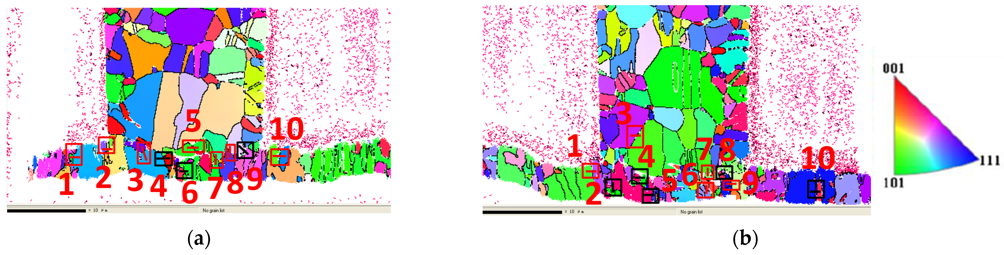
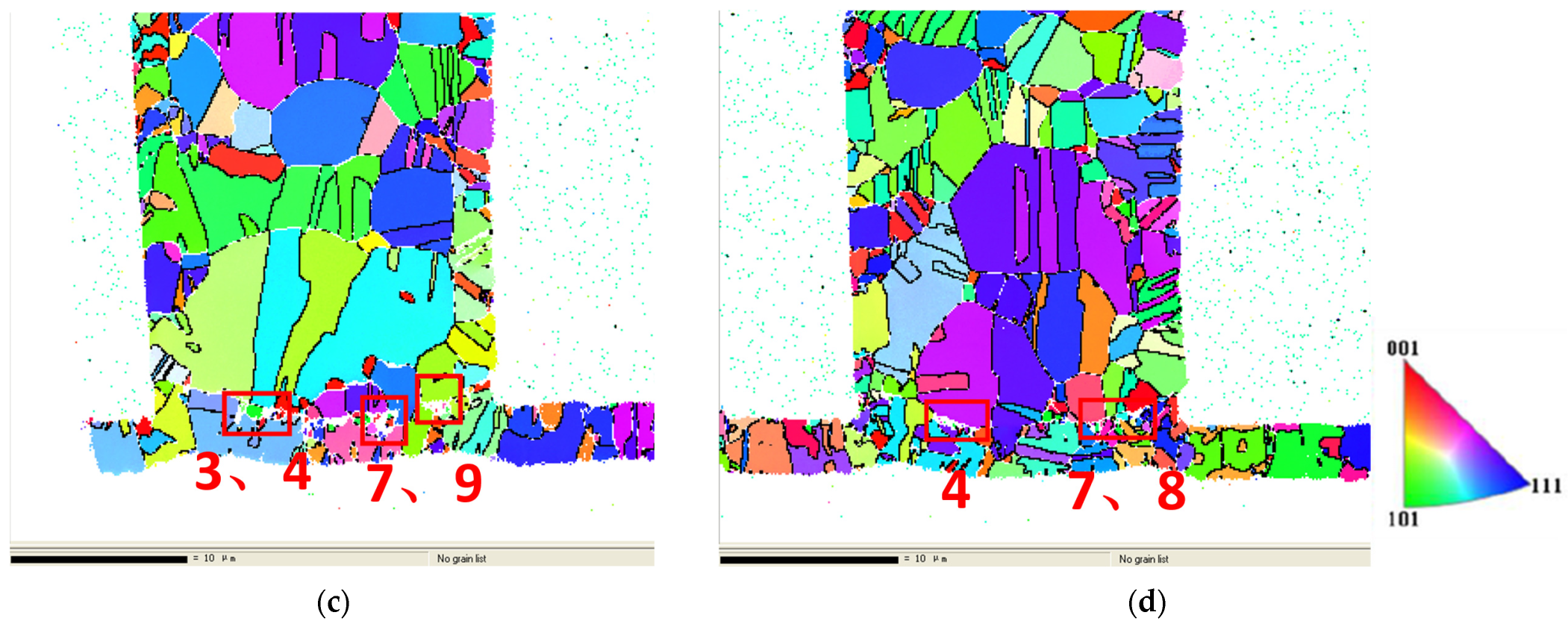
During the process of electromigration, the flow of current induces current density gradients and localized heating effects, leading to lattice distortions. These distortions result in changes to the microstructure within the grains of the TSV-metal line and the bottom metal line, consequently influencing grain orientation alterations. Such alterations exhibit a significant dependency on the angle between crystal orientation and the direction of the current. When the angle between the current direction and grain orientations [001] or [010] is larger, crystals are more prone to deviate towards directions with a smaller angle between the grain orientation and the current. This propensity arises because the current direction is precisely perpendicular to the <100> crystal plane, and within this crystal plane family, the atomic density is at its lowest, minimizing the energy required for electron migration. Hence, crystals tend to rotate toward the direction with the lowest energy requirement for electron migration.
(b)
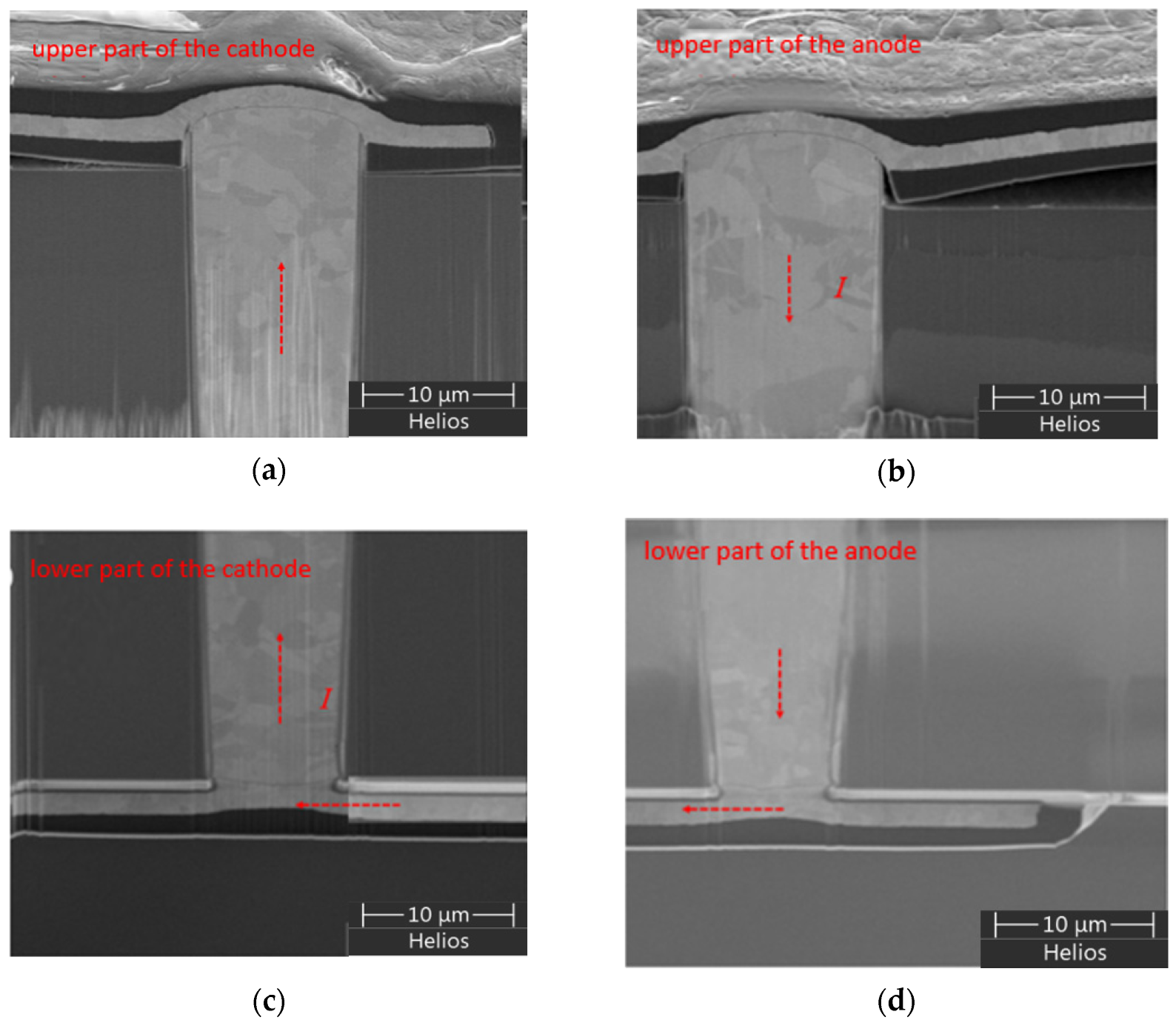
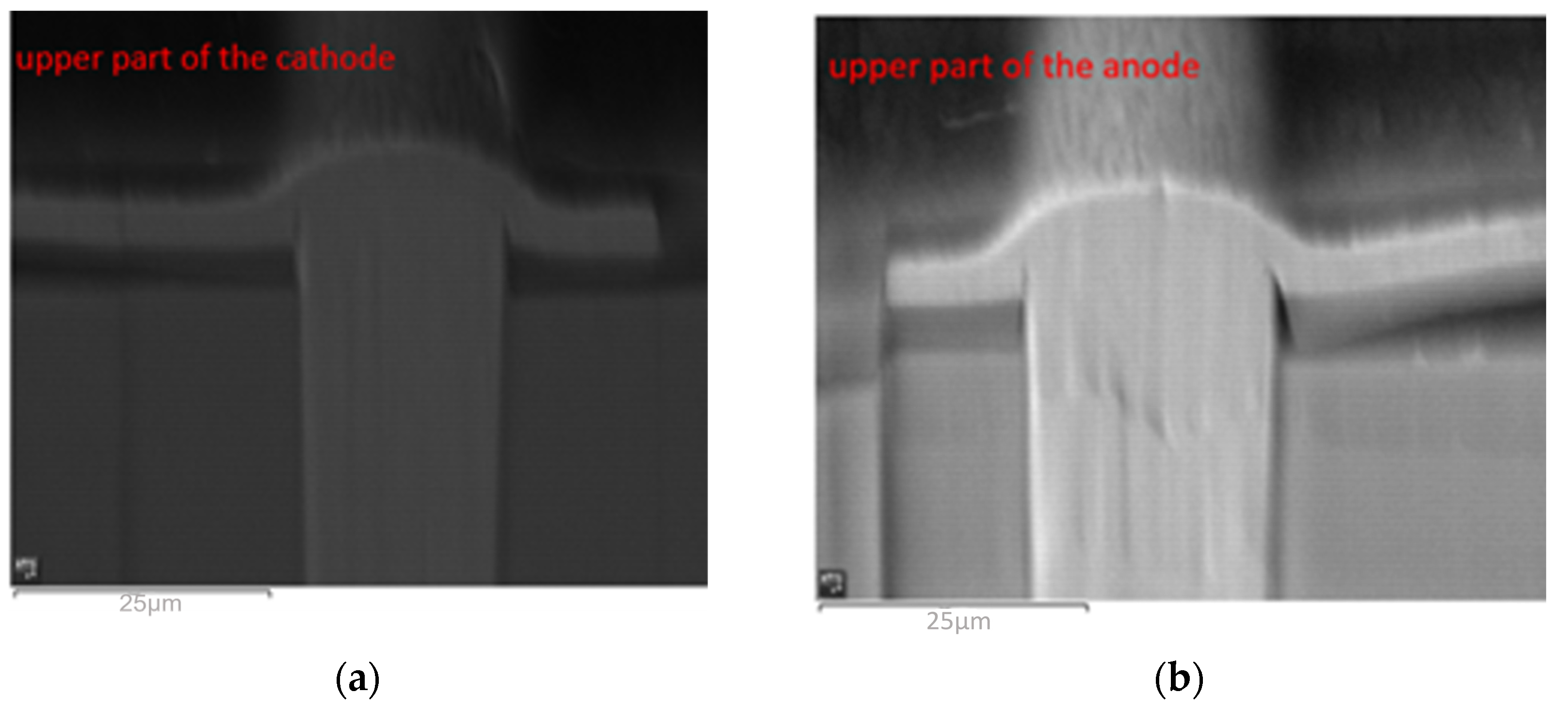
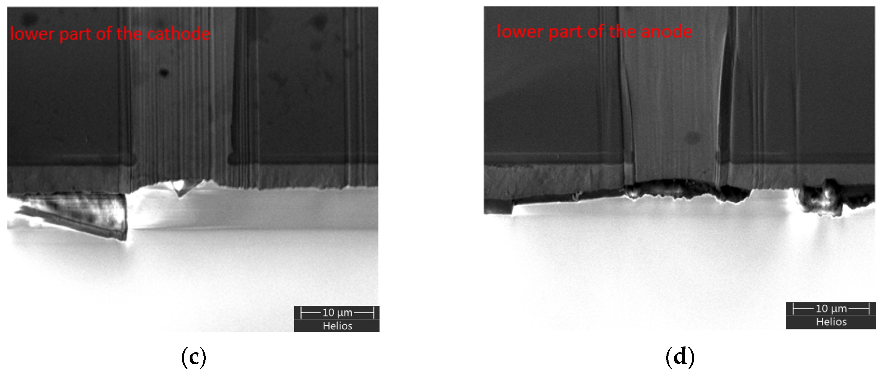
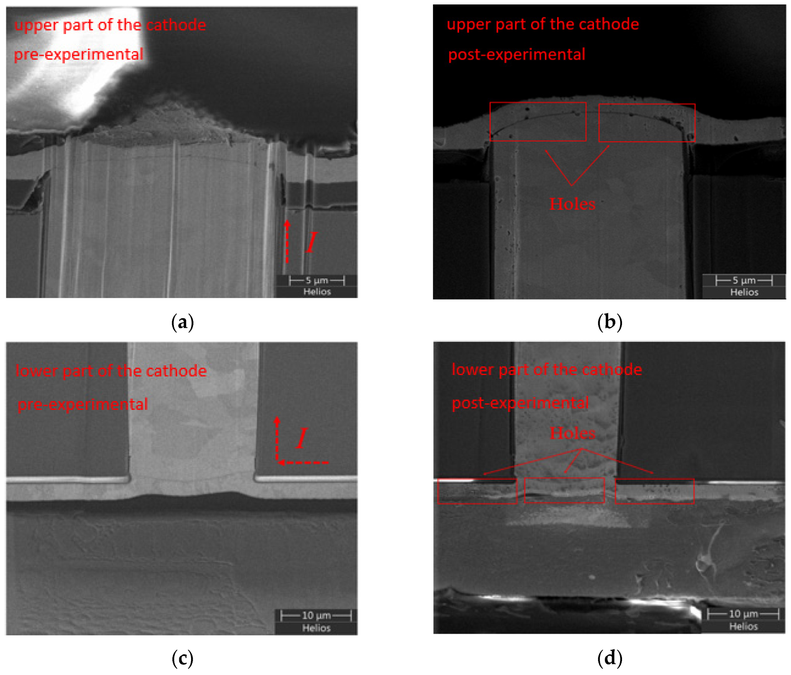
During the electromigration process in TSV samples, the regions where voids are more likely to form are typically located at the TSV-metal line and near its corners, especially in the upper section of the anode TSV, where a significant number of voids tend to develop. This phenomenon is influenced by the flow direction of grains and misorientation. The TSV-metal line area is typically characterized by high misorientation levels, and void formation tends to occur in regions with higher misorientation levels, particularly in areas where the grain boundary misorientation values were relatively larger before the experiment.

5. Comparative Discussion of Other Studies

A comparative analysis of [36,37] (Table 6) was conducted.
In summary, [36] provides an analysis of the microstructural evolution of TSV structures under different thermal loading conditions, investigates the mechanism of void generation in TSVs under thermal loading, and explores the electromigration mechanism of TSV-metal line structures through ex situ and in situ observations. It analyzes the causes of electromigration hillocks and voids in TSV-metal line structures, revealing the failure modes and mechanisms of TSV structures under different thermal and electromigration conditions. Ref. [37], through an electric-thermal-mechanical coupled analysis, elucidates the electromigration failure mechanism in TSV structures, with a focus on the influences of current crowding, stress concentration, and temperature and stress gradients on atomic flux divergence [36,37].
This paper: In comparison with other literature, this paper possesses the following advantages:
  • In-depth electromigration study: this paper extensively investigates the crystal orientation changes and electromigration failure in TSV-metal line structures induced by electrical currents, providing a deeper insight into the understanding of the failure mechanisms.
  • Exploration of the angle’s impact on crystal deviation: it emphasizes the significance of the angle between the direction of current flow and grain orientation in influencing crystal deviation, enhancing a detailed understanding of the failure mechanism.
  • Focus on the impact of high misorientation: it highlights the contribution of stress gradients induced by high misorientation to failure, providing valuable information for practical engineering applications.

Author Contributions

Conceptualization, T.G. and S.C.; methodology, L.X., X.L. and S.C.; software, T.G., X.L. and M.Z.; validation, L.X., J.Z.,S.C. and X.L.; formal analysis, T.G. and M.Z.; investigation, Z.W. and S.C.; resources, S.C. and X.L.; data curation, T.G., J.Z. and X.Y.; writing—original draft preparation, T.G., L.X. and S.C.; writing—review and editing, T.G., S.C. and X.L.; visualization, L.X., S.C. and M.Z.; supervision, S.C., X.L., X.Y. and Z.W.; project administration, S.C.; funding acquisition, S.C. and X.L. All authors have read and agreed to the published version of the manuscript.

Funding

This research received support from the National Natural Science Foundation of China (NSFC) under Grant No. 61804032; the Innovation and Entrepreneurship Leading Team Zengcheng under Grant No. 202102001; and the Natural Science Foundation of Fujian Province, China (Grant No. 2022J011264).

Data Availability Statement

Data are contained within the article.

Conflicts of Interest

The authors declare no conflict of interest.

References

  1. Lau, J.H. Overview and outlook of through-silicon via (TSV) and 3D integrations. Microelectron. Int. 2011, 62, 437–449. [Google Scholar] [CrossRef]
  2. Tu, K.N. Reliability challenges in 3D IC packaging technology. Microelectron. Reliab. 2011, 51, 517–523. [Google Scholar] [CrossRef]
  3. Xu, Z.; Lu, J.Q. High-speed design and broadband modeling of through-strata-vias (TSVs) in 3D integration. IEEE Trans. Compon. Packag. Manuf. Technol. 2011, 1, 154–162. [Google Scholar] [CrossRef]
  4. Jang, Y.J.; Sharma, A.; Jung, J.P. Advanced 3D Through-Si-Via and Solder Bumping Technology: A Review. Materials 2023, 16, 7652. [Google Scholar] [CrossRef] [PubMed]
  5. Wang, J.; Duan, F.; Lv, Z.; Chen, S.; Yang, X.; Chen, H.; Liu, J. A Short Review of Through-Silicon via (TSV) Interconnects: Metrology and Analysis. Appl. Sci. 2023, 13, 8301. [Google Scholar] [CrossRef]
  6. Tian, W.; Wu, S.; Li, W. Research of Vertical via Based on Silicon, Ceramic and Glass. Micromachines 2023, 14, 1391. [Google Scholar] [CrossRef] [PubMed]
  7. Chang, Y.-J.; Ko, C.-T.; Yu, T.-H.; Chiang, C.-H.; Chen, K.-N. Backside-process-induced junction leakage and process improvement of cu TSV based on Cu/Sn and BCB hybrid bonding. IEEE Electron. Device Lett. 2013, 34, 435–437. [Google Scholar] [CrossRef]
  8. Nakamura, T.; Kitada, H.; Mizushima, Y.; Maeda, N.; Fujimoto, K.; Ohba, T. Comparative study of side-wall roughness effects on leakage currents in through-silicon via interconnects. In Proceedings of the IEEE International 3D Systems Integration Conference (3D IC), Osaka, Japan, 31 January–2 February 2012; pp. 1–4. [Google Scholar]
  9. De Wolf, I.; Jacobs, K.J.; Orozco, A. Magnetic field imaging and light induced capacitance alteration for failure analysis of cu-TSV interconnects. Microelectron. Reliab. 2020, 114, 113780. [Google Scholar] [CrossRef]
  10. Rui, M.; Meiying, S.; Xiaofang, L. Finite Element Analysis of Influencing Factors on TSV Electromigration. Electron. Compon. Mater. 2019, 38, 93–97. [Google Scholar]
  11. Chen, S.; Jian, X.; Li, K. Effect of temperature cycling on the leakage mechanism of TSV liner. Microelectron. Reliab. 2023, 141, 114889. [Google Scholar] [CrossRef]
  12. Gousseau, S.; Bouchu, D.; Farcy, A.; Montmitonnet, P.; Inal, K.; Bay, F.; Zelsmann, M.; Picard, E.; Salaun, M. Electromigration-induced failure in operando characterization of 3D interconnects: Microstructure influence. Microelectron. Reliab. 2015, 55, 1205–1213. [Google Scholar] [CrossRef]
  13. Zhaohui, C. High-Power LED Packaging and Silicon Through-Silicon via (TSV) Three-Dimensional Packaging Process and Reliability Numerical Simulation and Experimental Study; Shanghai Jiao Tong University: Shanghai, China, 2012. [Google Scholar]
  14. Pak, J.; Pathak, M.; Lim, S.K.; Pan, D.Z. Modeling of electromigration in through-silicon-via based 3D IC. In Proceedings of the IEEE Electronic Components & Technology Conference, Buena Vista, FL, USA, 31 May–3 June 2011; pp. 1420–1427. [Google Scholar]
  15. Frank, T.; Moreau, S.; Chappaz, C.; Arnaud, L.; Leduc, P.; Thuaire, A.; Anghel, L. Electromigration behavior of 3D-IC TSV interconnects. In Proceedings of the IEEE Electronic Components and Technology Conference, San Diego, CA, USA, 29 May–1 June 2012; pp. 326–330. [Google Scholar]
  16. Zisser, W.; Ceric, H.; Weinbub, J.; Selberherr, S. Electromigration reliability of open TSV structures. Microelectron. Reliab. 2014, 54, 2133–2137. [Google Scholar] [CrossRef]
  17. Rovitto, M.; Zisser, W.H.; Ceric, H.; Grasser, T. Electromigration modelling of void nucleation in open Cu-TSVs. In Proceedings of the IEEE 16th International Conference on Thermal, Mechanical and Multi-Physics Simulation and Experiments in Microelectronics and Microsystems, Virtual, 19–22 April 2015; pp. 1–5. [Google Scholar]
  18. Hao, N. Reliability Simulation and Lifetime Prediction of TSV Structures under Multi-Stress Coupling; Xidian University: Xi’an, China, 2022. [Google Scholar]
  19. Bing, L. Research on the Nanomachining Mechanism Based on Scanning Electron Microscopy; Tianjin University: Tianjin, China, 2015. [Google Scholar]
  20. Yongmei, Y. Study on the Microstructure and Texture Evolution of Fe-3%Si Steel Strip in TSCR Process; Northeastern University: Shenyang, China, 2008. [Google Scholar]
  21. Fan, P. Research on Phase Identification and Orientation Analysis Methods Using Electron Backscatter Diffraction (EBSD); University of Chinese Academy of Sciences: Beijing, China, 2021. [Google Scholar]
  22. Ping, Y. Electron Backscatter Diffraction Technology and Its Applications; Metallurgical Industry Press: Beijing, China, 2007; pp. 51–53. [Google Scholar]
  23. Yulong, L. Research on the Plane Strain Plastic Deformation Mechanism and Microstructure Evolution of Ni-Ti-Fe Shape Memory Alloy; Harbin Engineering University: Harbin, China, 2017. [Google Scholar]
  24. Yanling, Y. Preparation of Nickel and Nickel-Iron Nanomaterials and Research on Cold Rolling-Annealing Textures; Northeastern University: Shenyang, China, 2009. [Google Scholar]
  25. Yu, T. The Influence of Grain Number and Intermetallic Compounds on the Electromigration Behavior of Sn-Based Solder Joints; Beijing University of Technology: Beijing, China, 2020. [Google Scholar]
  26. Shihua, Y. Micro-Mechanical Behavior of SnAgCu/Cu Solder Joints with Limited Grains; Harbin Institute of Technology: Harbin, China, 2010. [Google Scholar]
  27. Zhao, J.; Huang, M.; Zhao, N.; Zhang, Z. Effect of Sn grain orientation on Cu diffusion in SnAgCu solder interconnect undergoing electromigration. In Proceedings of the 16th International Conference on Electronic Packaging Technology, Changsha, China, 11–14 August 2015; pp. 1275–1278. [Google Scholar]
  28. Chen, J.Q.; Liu, K.L.; Guo, J.D.; Ma, H.C.; Wei, S.; Shang, J.K. Electromigration anisotropy introduced by tin orientation in solder joints. J. Alloys Compd. 2017, 703, 264–271. [Google Scholar] [CrossRef]
  29. Shen, Y.A.; Chen, C. Effect of Sn grain orientation on formation of Cu6Sn5 intermetallic compounds during electromigration. Scr. Mater. 2017, 128, 6–9. [Google Scholar] [CrossRef]
  30. Lu, M.; Shih, D.Y.; Lauro, P.; Goldsmith, C.; Henderson, D.W. Effect of Sn grain orientation on electromigration degradation mechanism in high Sn-based Pb-free solders. Appl. Phys. Lett. 2008, 92, 211909. [Google Scholar] [CrossRef]
  31. Deng, S.; Li, R.; Yuan, T. The preferential growth behaviors of the intermetallics at the W/Co interface during spark plasma sintering. Appl. Phys. Lett. 2020, 117, 194102. [Google Scholar] [CrossRef]
  32. Baolin, G. Research on Electromigration Effects in Copper Interconnects with Lateral Redundancy; Dalian University of Technology: Dalian, China, 2016. [Google Scholar]
  33. Si, C. Research on the TSV-Cu Extrusion Behavior in Key Structures of Three-Dimensional Electronic Packaging; Beijing University of Technology: Beijing, China, 2017. [Google Scholar]
  34. Zhilyaev, A.P.; Sergeev, S.N.; Langdon, T.G. Electron backscatter diffraction (EBSD) microstructure evolution in HPT copper annealed at a low temperature. J. Mater. Res. Technol. 2014, 3, 338–343. [Google Scholar] [CrossRef]
  35. Jasionowski, R.; Zasada, D.; Polkowski, W. EBSD strain analysis of CuZn10 alloy in as-cast state and after plastic working and annealing during cavitational wear. Arch. Foundry Eng. 2013, 13, 53–60. [Google Scholar]
  36. Wei, Z.X. Microstructure Evolution and Mechanism Study of Copper-Filled Silicon Vias under Thermal and Electrical Conditions; Beijing University of Technology: Beijing, China, 2019. [Google Scholar]
  37. Zhang, Y.; Yu, S.; Su, D.; Shen, Z. Finite element modeling on electromigration of TSV interconnect in 3D package. In Proceedings of the IEEE 20th Electronics Packaging Technology Conference (EPTC), Singapore, 4–7 December 2018. [Google Scholar]
Figure 1. Schematic diagram of the TSV-metal line sample structure.
Crystals 14 00037 g001
Figure 2. TSV-metal line electromigration current direction: (a) samples A, B, and C; (b) sample D.
Crystals 14 00037 g002
Figure 3. TSV electromigration test platform: (a) Overall Diagram of TSV Electron Migration Test Platform; (b) Lake Shore CRX-6.5K Probe Station Sample Stage.
Crystals 14 00037 g003
Figure 4. TSV-metal line sample after bonding (a), surface morphology after grinding (b), and cross-sectional morphology (c).
Crystals 14 00037 g004
Figure 5. SEM Images of sample A before electromigration: (a,b) upper regions of the cathode and anode; (c,d) lower regions of the cathode and anode.
Crystals 14 00037 g005
Figure 6. SEM images of sample A after electromigration: (a,b) upper regions of the cathode and anode; (c,d) lower regions of the cathode and anode.
Crystals 14 00037 g006aCrystals 14 00037 g006b
Figure 7. Relationship between sample coordinate axes and current direction in TSV.
Crystals 14 00037 g007
Figure 8. EBSD plots before and after electromigration of the upper part of the cathode of sample A: (a,b) before and after electromigration of the upper part of the cathode.
Crystals 14 00037 g008
Figure 9. EBSD plots before and after electromigration at the upper anode of sample A: (a,b) before and after electromigration at the upper anode.
Crystals 14 00037 g009
Figure 10. SEM images of the lower part of the cathode TSV in sample B before and after electromigration: (a) before electromigration, (b) after electromigration, (c) left side after electromigration, and (d) middle after electromigration.
Crystals 14 00037 g010
Figure 11. SEM images of the lower part of the anode TSV in sample B before and after electromigration: (a) before electromigration, (b) after electromigration, (c) left side after electromigration, (d) middle after electromigration, and (e) right side after electromigration.
Crystals 14 00037 g011
Figure 12. EBSD images of the lower sections of TSV for Sample B: (a) cathode before the experiment, (b) anode before the experiment, (c) cathode after the experiment, and (d) anode after the experiment.
Crystals 14 00037 g012aCrystals 14 00037 g012b
Figure 13. Misorientation maps of the lower sections of TSV under the cathode (a) and anode (b) before electromigration.
Crystals 14 00037 g013
Figure 14. SEM images of the cathode TSV in sample C before and after electromigration: (a) upper part before electromigration and (b) after electromigration, (c) lower part before electromigration and (d) after electromigration.
Crystals 14 00037 g014
Figure 15. EBSD images of the cathode TSV in sample C before and after electromigration: (a) upper part before electromigration, (b) upper part after electromigration, (c) lower part before electromigration, and (d) lower part after electromigration.
Crystals 14 00037 g015
Figure 16. SEM images of sample D at various locations before and after electromigration: (a) upper part of the anode before electromigration, (b) upper part of the anode after electromigration, (c) lower part of the anode before electromigration, (d) lower part of the anode after electromigration, (e) lower part of the cathode before electromigration, and (f) lower part of the cathode after electromigration.
Crystals 14 00037 g016aCrystals 14 00037 g016b
Figure 17. EBSD images of various sections of sample D before and after electromigration: (a) anode upper portion before, (b) anode upper portion after, (c) anode lower portion before, (d) anode lower portion after, (e) cathode lower portion before, and (f) cathode lower portion after.
Crystals 14 00037 g017
Figure 18. Misorientation maps of the cross-sections for samples C and D before electromigration are as follows: the upper section of the cathode for sample C (a), the lower section of the cathode for sample C (b), the upper section of the anode for sample D (c), the lower section of the anode for sample D (d), and the lower section of the cathode for sample D (e).
Crystals 14 00037 g018aCrystals 14 00037 g018b
Table 1. Cross-sectional dimensions of TSV-metal line.
LayerMaterialThickness (μm)Tolerance (μm)
D1_TJSR51005±1.5
M1_TCu3±1
SiO2SiO22±10%
TSVCu100±10
D1_BJSR51003.5±1.5
M1_BCu3±1
D2_BJSR51005±1.5
BumpCu50±5
Ni3±1
SnAg27±3
Table 2. Four test conditions.
SampleCurrentTemperatureTime
A0.159 A (current density 1.0 × 10⁵ A/cm2)100 °C210 h
B0.785 A (current density 5.0 × 10⁵ A/cm2)100 °C210 h
C1.59 A (current density 1.0 × 10⁶ A/cm2)100 °C210 h
D1.59 A (current density 1.0 × 10⁶ A/cm2)100 °C210 h
Table 3. Misorientation of grain boundaries at positions 1–10 in Figure 12a,b.
PlacementFigure 12a Misorientation of
Grain Boundaries (°)
Figure 12b Misorientation of
Grain Boundaries (°)
127.6340.13
238.9438.80
359.8837.57
459.9659.96
539.0531.36
639.1338.43
755.5951.66
825.4059.94
959.6144.25
1038.7735.59
Table 4. The misorientation of grain boundaries in Figure 15a,c.
PlacementFigure 15a Misorientation of
Grain Boundaries (°)
Figure 15c Misorientation of
Grain Boundaries (°)
152.8229.04
259.9338.91
338.9631.42
425.8934.51
525.4428.95
648.524.24
736.5948.02
837.0540
9\39
Table 5. The misorientation of grain boundaries in Figure 17a,c,e.
PlacementFigure 17a Misorientation of Grain Boundaries (°)Figure 17c Misorientation of Grain Boundaries (°)Figure 17e Misorientation of Grain Boundaries (°)
159.2731.7731.73
259.6159.8950
335.916059.63
459.8959.8658.63
558.3659.8858.95
639.1659.7941.85
759.8337.9614.26
858.8559.7853.12
932.5459.9256.64
10\59.8759.98
11\59.9259.83
12\31.3159.89
13\\30.83
Table 6. Comparison table between this paper and other references.
LiteratureFailure ModeFailure Mechanism
1. Microstructure Evolution and Mechanism Study of Copper-Filled Silicon Through-Silicon Vias under Thermal and Electrical Conditions.1. Overall and local extrusion of TSV-Cu.
2. Formation of voids.
1. Mechanism of TSV-Cu extrusion: related to thermal stress, stress relaxation, surface grain boundary characteristics, and grain morphology.
2. Mechanism of void generation: greater stress concentration and grain boundary energy reduce the nucleation barrier, increasing the probability of void formation in the corresponding locations.
2. Finite element modeling on electromigration of TSV interconnect in 3D package.Electromigration failure.1. Current crowding and stress concentration.
2. Temperature gradient.
3. Stress gradient.
3. Research on Crystal Structure Evolution and Failure Mechanism during TSV-metal line Electromigration Process (this article).1. Current induces a change in crystal grain orientation.
2. Regions with high misorientation are prone to forming voids.
1. Current-induced crystal orientation change.
2. Crystal deviation mechanism.
3. High misorientation causing stress gradient.
4. Aggravation of failure with increasing current density.
Disclaimer/Publisher’s Note: The statements, opinions and data contained in all publications are solely those of the individual author(s) and contributor(s) and not of MDPI and/or the editor(s). MDPI and/or the editor(s) disclaim responsibility for any injury to people or property resulting from any ideas, methods, instructions or products referred to in the content.

