Article

3D Optical Wedge and Movable Optical Axis LC Lens

1
School of Precision Instrument and Opto-Electronics Engineering, Ministry of Education, Tianjin University, Tianjin 300072, China
2
Key Laboratory of Optoelectronic Information Technical Science, Ministry of Education, Tianjin University, Tianjin 300072, China
*
Author to whom correspondence should be addressed.
Crystals 2024, 14(10), 843; https://doi.org/10.3390/cryst14100843
Submission received: 9 September 2024 / Revised: 26 September 2024 / Accepted: 26 September 2024 / Published: 27 September 2024
(This article belongs to the Collection Liquid Crystals and Their Applications)

Abstract

:
Current liquid crystal (LC) lenses cannot achieve lossless arbitrary movement of the optical axis without mechanical movement. This article designs a novel bottom electrode through simulation and optimization, which forms a special LC lens with an Archimedean spiral electrode, realizing a 3D LC wedge and an arbitrarily movable LC lens. When only the bottom electrode is controlled, it achieves a maximum beam steering angle of 0.164°, which is nearly an order of magnitude larger than the current design. When the top and bottom electrodes are controlled jointly, a 0.164° movement of the lens optical axis is achieved. With focal length varies, the movement of the optical axis ranges from zero to infinity, and the lens surface remains unchanged during movement. The focus can move in a 3D conical area. When the thickness of the LC layer is 30 μm, the fastest response time reaches only 0.635 s, much faster than now.

1. Introduction

Nowadays, tunable optical wedges and optical axis motion (OAM) lenses are capable of achieving optical image stabilization (OIS) [1,2,3,4], auto-focus [5], super-resolution imaging [6,7,8], 3D reconstruction [9,10,11], and optical tweezers [12,13], etc. Meanwhile, the movement of traditional solid lenses needs mechanical movement, thereby increasing power consumption, occupying space, and presenting low tuning efficiency [14].
Traditional adaptive optics—a technology aimed at improving the performance of optical systems—can indeed achieve beam steering [15] and focusing [16,17,18], but it requires the control of multiple mirrors to construct a deformable mirror surface, resulting in high costs and complex structure. A comprehensive system is also indispensable for real-time feedback, including a wavefront detector, wavefront controller, and wavefront corrector [19], which leads to a large size. Therefore, it is usually used in fields such as astronomy, which requires high precision and multi-discipline. However, LC lenses have significant advantages in terms of miniaturization, are lightweight, and have a low cost when applied voltage of less than 10 V [20]. The millimeter-level dimensions and micron-level thickness render the LC lens portable and suitable for mobile phones and other small devices, making it perfectly convenient in life.
LC devices are the typical representative of novel adaptive optics and function as a phase modulation element. The researches encompass LC beam deflectors [21,22] and LC zoom lenses [23,24]. The beam deflectors are classified into refractive wedges and diffraction gratings [22]. The former generates a small refractive angle yet incurs a relatively small loss of light energy, while the latter exhibits a large angle but has multiple diffraction orders, resulting in a more significant light loss. The research on refractive LC wedges is gradually becoming more comprehensive. Love [25] and Hands [26] have achieved beam steering in 1D with a 0.01° steering angle and in 2D with a 0.024° steering angle. Kotova [27] employed a modal four-electrode device to observe the 3D continuous optical deflection experimentally. Nevertheless, the deflection theory was not improved until Xu [28], accomplishing 0.048° beam deflection.
The LC zoom lens, initially proposed by Sato and Ye [20,23,29,30,31], is capable of adjusting the focal length and optical axis without mechanical movement. Nevertheless, the OAM lens exhibits poor performance and significant aberrations, and it has difficulty maintaining shape during movement. Meanwhile, the modal electrodes produce an uneven and unstable voltage distribution. With the advancement of LC pattern electrodes with micro-structured [32,33,34,35,36], the voltage across the aperture can be precisely characterized by the expression. However, independent research on LC devices has resulted in low utilization efficiency of layer electrodes.
Therefore, through multi-simulations and optimizations, this paper proposes a novel LC lens with a movable optical axis that can achieve the movement of focus in 3D space without mechanical movement. It possesses the merits of adjustable focal length, lightweight, compact structure, no mechanical movement, and low power consumption. This paper elaborates on the design principle, working principle, and driving method of the electrodes and fabricates a liquid crystal lens with a liquid crystal layer of 30 μm. The interference fringes and positions during the movement process were recorded, and they were compared with the theoretical values.

2. Principle

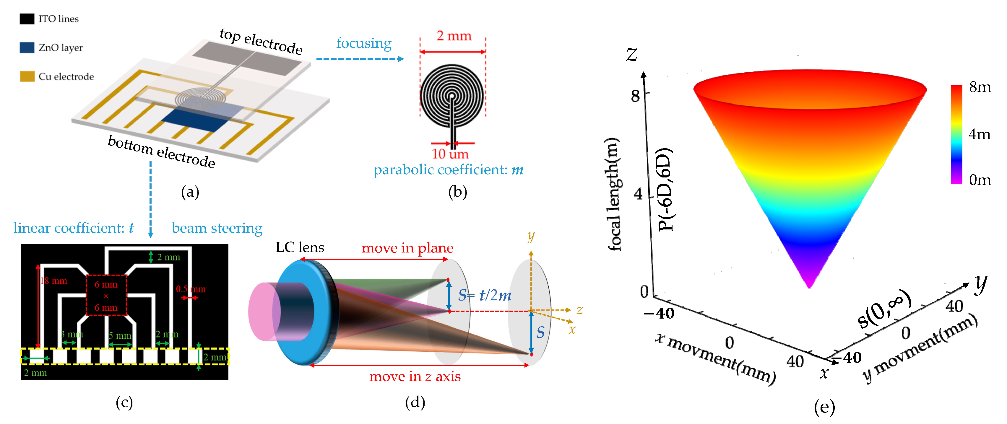
2.1. Electrode Structure and Process

For the OAM-LC lens, the device structure is presented in Figure 1a, comprising five parts: glass, top electrode, LC layer, bottom electrode, and glass. The top electrode, as shown in Figure 1b, is an Archimedean spiral with equal spacing, which is designed based on the patterned electrode theory to achieve low aberration focusing [37]. The bottom electrode is designed based on vector synthesis and modal electrode theory [38], generating a planar phase difference to achieve beam steering and focus movement. The bottom electrode structure is shown in Figure 1c. When the top and bottom electrodes are jointly controlled, as depicted in Figure 1d, the focus can move within the 3D space, and its movement range lies within the conical area presented in Figure 1e. The dioptre power is within ±6D, the vibration of the l optical axis ranges from 0.164°, and the movement of the optical axis can reach infinity.
It is worth noting that the bottom electrode is composed of copper (Copper) and zinc oxide (Zinc Oxide); hence, the size and brief manufacturing process of the electrode must be explained. The size of the glass is 25 mm × 20 mm. Since there is an extremely negligible voltage drop across the copper wires, it is sufficient to ensure that they can be connected. The current design of copper wires features a width of 0.5 mm, with the central Zinc Oxide region being 6 mm×6 mm. The total radius of the top electrode is 1 mm, as depicted in Figure 1b, with electrode widths and gaps both 10 μm.
We simulated the voltage distribution by COMSOL, and a perfect oblique planar phase difference was generated in the central 2 mm × 2 mm region within the ZnO area, as shown in Figure 2a,b. This implies that the top electrode generates a parabolic voltage distribution while the bottom electrode generates a planar voltage distribution, as shown in Figure 2c. The voltage difference within the LC cell is determined by the top and bottom electrodes.
The bottom electrode is developed using two photolithographic steps for the deposition of high-resistance copper and zinc oxide films. The rotating speed of the spin-coated photoresist is 6000 RPM. The deposition duration for copper and zinc oxide high-resistance films is approximately 30 min and 35 min, respectively. The thickness of the zinc oxide film is approximately 25 nm. The resistance εrcu of the copper electrode is approximately 300 Ω, and the εrZnO of the zinc oxide region is approximately 1 MΩ. The resistance ratio between the two is approximately 103. In accordance with the simulation in Figure 2d, when the sheet resistance ratio (εr) between the two exceeds 103, the copper will scarcely generate a voltage drop.

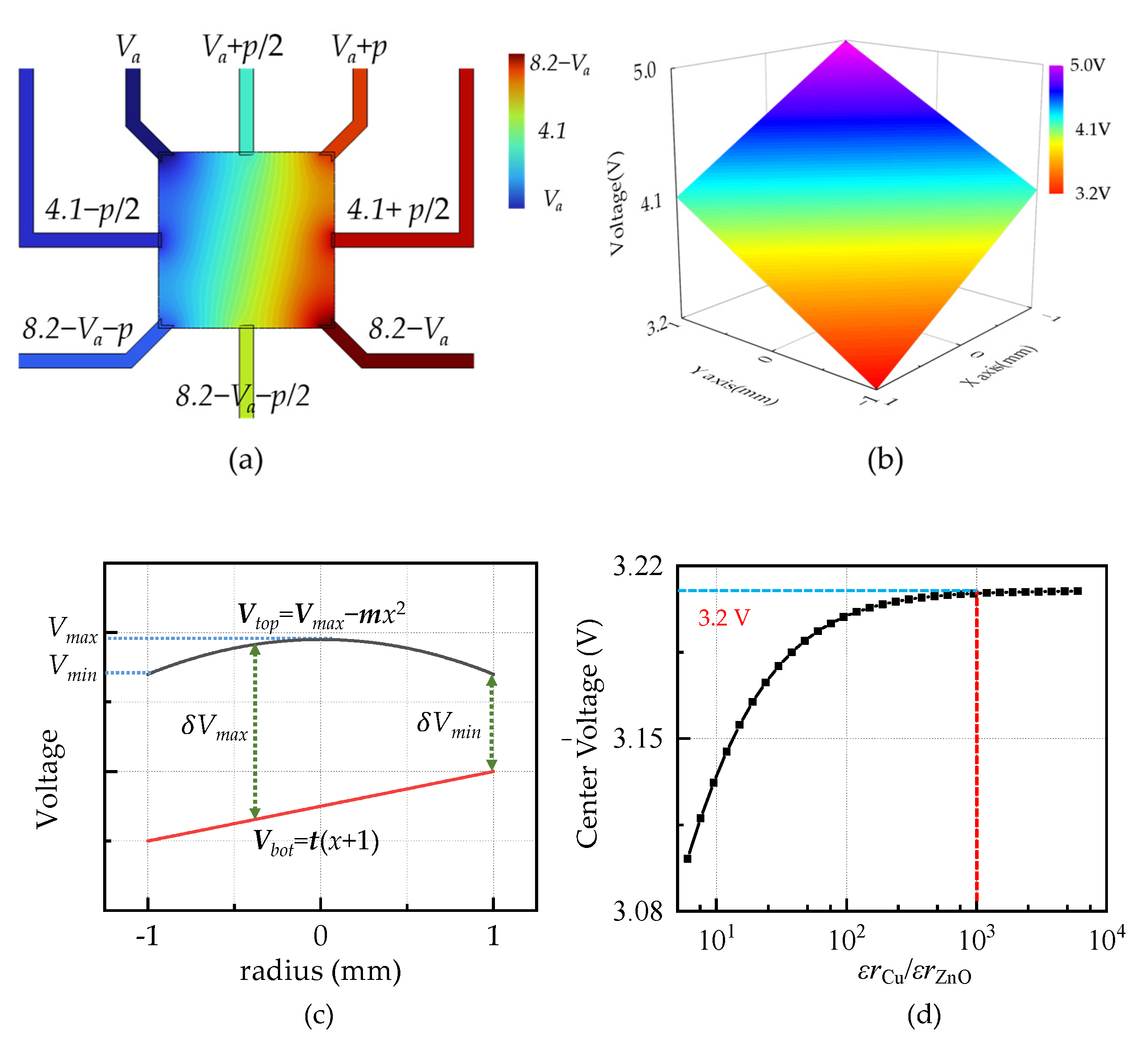
2.2. Function and Working Principle

This structure can realize an optical-axis-movable LC lens (OAM LC lens), which is a highly significant function. OAM lenses can improve the imaging performance of the optical system through adaptive zooming and simultaneously eliminate image shifts induced by the optical axis shift and tilt of the camera. Hence, the system holds potential applications in optical image stabilization (OIS). Thus, the system can realize multiple functions, and the specific functions and theoretical derivations will be expounded in detail in the subsequent sections.
3D Optical wedge: According to the simulation in Figure 2b, the center of the bottom electrode can generate a planar phase profile, which means an optical wedge can be made. Moreover, the steering angle θw and azimuth angle θa are controlled by two parameters, Va and p. The θw and θa are expressed as:
θ a = arctan ( N λ D i a m e t e r ) = arctan ( Δ n h L C D i a m e t e r )
θ a = arctan ( Δ n x / Δ n y )
N: the number of stripes, λ: laser wavelength; Δn: refractive index difference; hLC: LC layer thickness.
Zoom imaging: The voltage distribution of the top electrode and bottom electrode are parabolic and planar, respectively, as we can see in Figure 2c.
The voltage difference within the aperture can be expressed as Equation (2):
v = V m a x m x 2 t ( x + 1 )
m: the parabolic coefficient (V·mm−2); t: the linear coefficient (V·mm−1); Vmax: the maximum voltage on the top electrode; Vmin: the minimum voltage on the top electrode; x (mm) is the position of a point within the aperture. To generate parabolic and planar phase profiles, all voltage difference values within the aperture must fall within the linear response region of the LC material [39]. If t = 0, the voltage difference within the aperture is a parabolic distribution to be a lens with a small wavefront RMS error (<0.05 λ).
OAM lens: by transforming the Equation (3), the voltage difference can be expressed as Equation (4):
v = ( V m a x t + t 2 4 m ) m ( x + t 2 m ) 2
From Equation (4), the axis of the parabolic function has shifted, but its shape has not changed with parabolic coefficient m remains. This implies that when the top and bottom electrodes are jointly controlled, they can be OAM LC lenses and remain unchanged during the movement of the optical axis. The movement of the optical axis is obtained.
s = t 2 m
s: the movement of the optical axis of the OAM lens. From Equation (5), the optical axis of the lens can move to any position, but if it is too far away, it is meaningless for the 2 mm × 2 mm lens. Therefore, achieving movement within the 2 mm × 2 mm aperture is sufficient.
Offset image shifts caused by optical axis vibration: When photographing images of distant objects, minor shifts in the imaging system induced by external forces will give rise to the vibration of the lens. If the conventional solid lens is still employed, the imaging position will undergo displacement. The prevailing OIS technology is cropping the image. Nevertheless, by utilizing the aforementioned OAM lens, optical image stabilization can be accomplished without any information loss and mechanical movement through the lens moving in the opposite direction. Its working principle is shown in Figure 3a.
The offset of the image can also be explained by the following expression. The image movement is equal to the steering angle multiplied by the focal length. The focal length of the LC lens is expressed as:
f = r 2 2 d × Δ n
The offset of the image is:
Δ h = f tan θ = t 2 m = s
By combining Equations (5) and (7), the offset of the image is exactly equal to the shift of the lens optical axis, and they compensate for each other.
Overall, this is why the lens can be used for OIS. It can eliminate parallel movement of the optical axis and compensate for image offset caused by optical axis vibration. This shows the multifunctionality of the OAM lens.

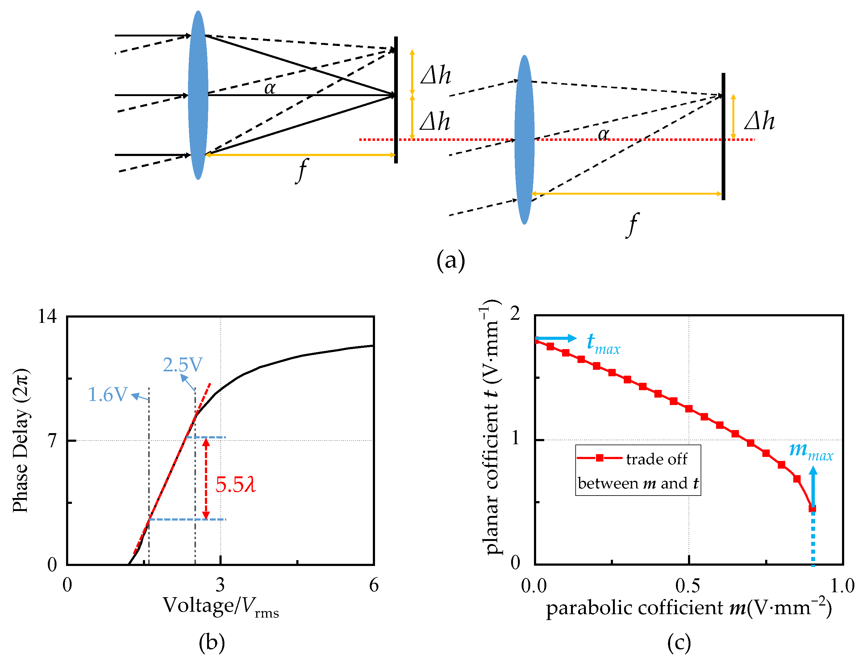
2.3. Driving Voltage Condition

Within the aperture, the voltage difference must fall within the linear response region (1.6~2.5 V) of the LC material depicted in Figure 3b. Therefore, it is necessary to satisfy the condition that δVmaxδVmin≤ 5 V–3.2 V. Moreover, the driving voltages require rigorous calculations.
δ V m a x = V m a x m ( t 2 m ) 2 t ( t 2 m + 1 ) = V max + t 2 4 m t 5
δ V m i n = V m a x m r 2 ( r + 1 ) t 3.2
δVmax: the maximum voltage difference in the 2 mm × 2 mm aperture; δVmin: the minimum voltage difference in the 2 mm × 2 mm aperture; r is the radius of the LC lens. Combining Equations (8) and (9), we can obtain the trade-off between m and t as shown in Equation (10):
4 m 2 + ( 4 t r 7.2 ) m + ( t r ) 2 0
Thus, the driving voltage range is expressed as follows:
V m i n 3.2 + 2 t r
m - ( 4 t r 7.2 ) + 7.2 × ( 7.2 8 t r ) 8
In this article, the radius of the OAM LC lens is 1 mm. The trade-off between m and t is depicted in Figure 3c.

3. Experiment and Result

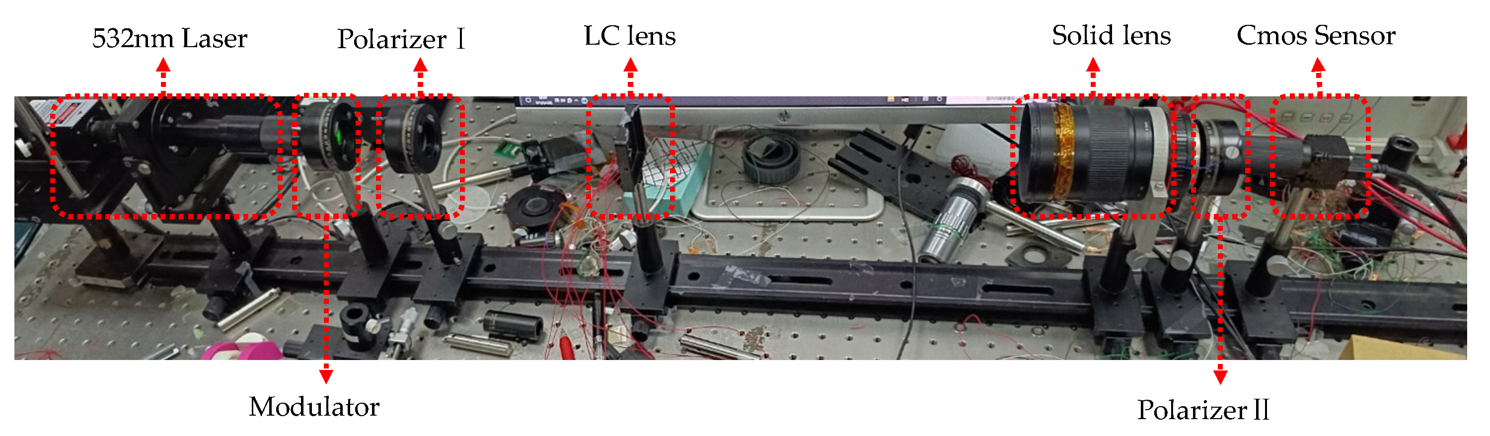
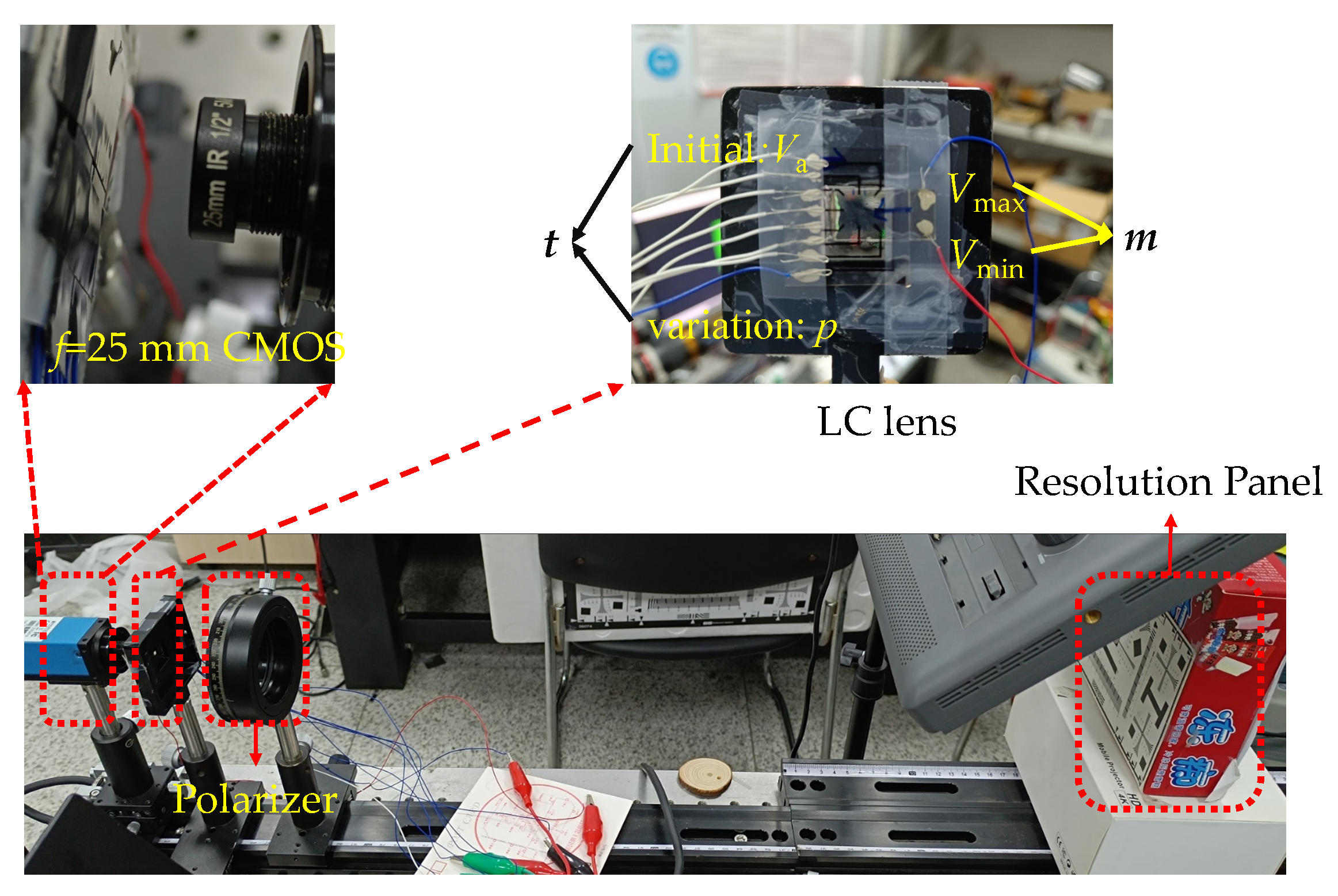
3.1. Experimental Setup

We designed two interference optical paths in Figure 4 and Figure 5 for the experiment. The device in Figure 4 was used to record the fringes to verify the feasibility of the OAM lens. The laser wavelength is 532 nm, and the modulator is used to adjust the intensity of the laser. When the laser passes through the polarizer I, it is decomposed into two orthogonal components. The first one sees the LC ordinary refractive index, which is uniform. However, the second one shows the LC’s extraordinary refractive index, which is affected by the applied voltages. The two components have phase differences; as they pass through the polarizer II, the interference fringes are captured by the CMOS camera.
The setup in Figure 5 was used to capture the image shifts caused by the OAM lens in the imaging system. We place the OAM lens in the imaging system, and the optical wedge will deflect the incident light, causing an image shift.
The prepared LC lens is shown in Figure 5. The left electrodes control the bottom voltage to achieve the OAM. The two left electrodes control the upper voltage and the focusing effect of the LC. The positive nematic LC material used in the experiment is HTW 148700-100, produced by Hecheng Display Technology Co., Ltd. from Yangzhong, Jiangsu China, whose optical birefringence Δn = 0.259. The linear response range of this LC material is measured using the method reported in [40], which is 1.6~2.5 Vrms. Then, the driving voltage difference falls within this range to generate a specific phase profile. The driving voltages are square waves. Therefore, 1.6–2.5 Vrms is equivalent to 3.2–5.0 Vpp, and the voltage mentioned below in the article is the Vpp. The frequency of the driving voltage is all 1 kHz in this work.

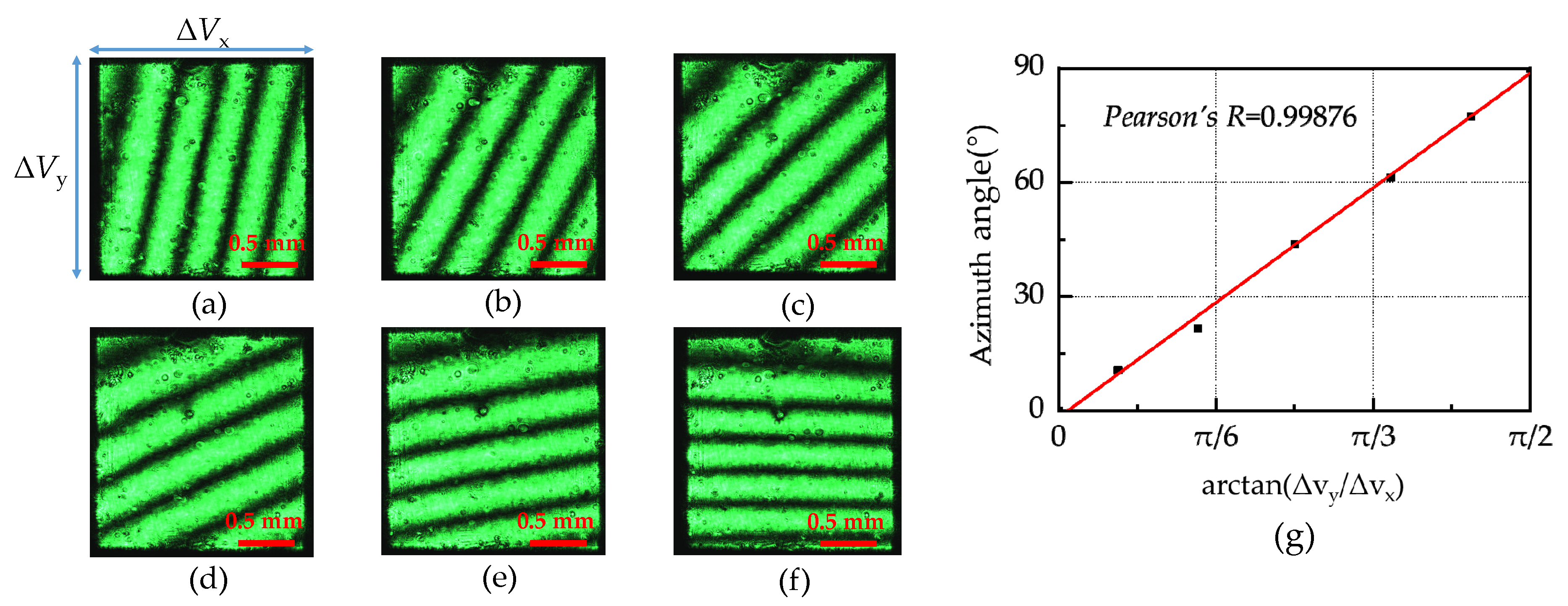
3.2. Analysis of Light Deflection Experiment

The driving voltage is related to two parameters, Va and p. Va determines the azimuth angle θa, and p determines the steering angle θw. The interference fringes of the 3D optical wedge are recorded in Figure 6a–f with different driving voltages listed in Table 1.
The results shown in Figure 6 demonstrated that the LC optical wedge adjusts from 0–90° as the fringes with different tilt angles. There are approximately 5.5 λ variations within the aperture, which means the wedge angle is 0.0838° from Equation (1).
According to the voltage from Table 1, the ratio of voltage drops across the XVx) and YVy) axis is related to the slope of the fringes. Due to the slope of the tilt fringes and the fact that the ratio may be infinite, they were processed by means of the inverse tangent function. A relationship between the azimuth angle and the ratio is plotted in Figure 6g, demonstrating a linear relationship in the form of a proportional function.
The proportional relationship means that the structure has the advantage of controlling the azimuth angle of the beam steering by applying voltage ΔVy and ΔVx across the electrode. The linear fit is as high as 0.999, nearly to 1.
The LC optical wedge is placed into the imaging system in Figure 5, and the practicability of the LC optical wedge is verified by the imaging resolution plate in the experiment. Figure 7e is the original state; the surrounding images are shifted by the wedge. The movement in Figure 7a–i is depicted in Figure 7j.
In the optical imaging system shown in Figure 5, the object distance is 700 mm, with a 25 mm lens employed, giving rise to a maximum image shift of 1 mm. According to geometric calculations, the maximum angular deviation in one direction can reach 0.164°.

3.3. Analysis of Off-Axis Focusing Experiment

It should be noted that when applying the voltage to the OAM lens, the trade-off between the m and t needs to be considered according to Equation (12), as shown in Figure 3c.
According to Equations (4) and (5), m determines the dioptre power, and m and t jointly determine the movement of the lens s, which means that the trade-off between the m and t leads a trade-off between the movement s and the dioptre power as depicted in Figure 8. The maximum dioptre power of the lens is ±6D. Once the OAM lens moves to infinity, the dioptre power is nearly 0, the movement can be calculated by Equation (6), and the fringes are parallel.
Four experiments were proposed with different values of m and t to demonstrate the OAM lens. Here, we define Sfigure as the real movement of the OAM lens in figures.

3.3.1. m and t at the Critical Condition

When the voltage differences within the aperture entirely fall within the linear response range of the LC material (1.6–2.5 Vrms), the LC lens can achieve the specific function. Hence, the critical conditions of m and n addressed in this article occur when δVmax = 2.5 Vrms and δVmin = 1.6 Vrms, as Equation (12) met the condition of equality. The values of m and t within the critical conditions are a must to guarantee that the voltage difference lies within the linear response range of the LC material. The critical condition of m and t is listed in Table 2, and the linear response region of the LC material is fully used (δVmax = 5.0 V, δVmin = 3.2 V), ensuring that at least five fringes can be observed in Figure 9.
From Figure 9a–i, the lens shifts from the aperture center. The movement of the OAM lens Sfigure is recorded by pixels, compared with the theoretical value s. The aberrations of the OAM lens were recorded to verify its feasibility as a lens in Figure 9j, and the aberrations were all less than 0.1 λ, which demonstrates the good imaging performance of the proposed OAM LC lens. Therefore, when the OAM lens moves unidirectionally at critical conditions, the RMS error is no longer recorded.

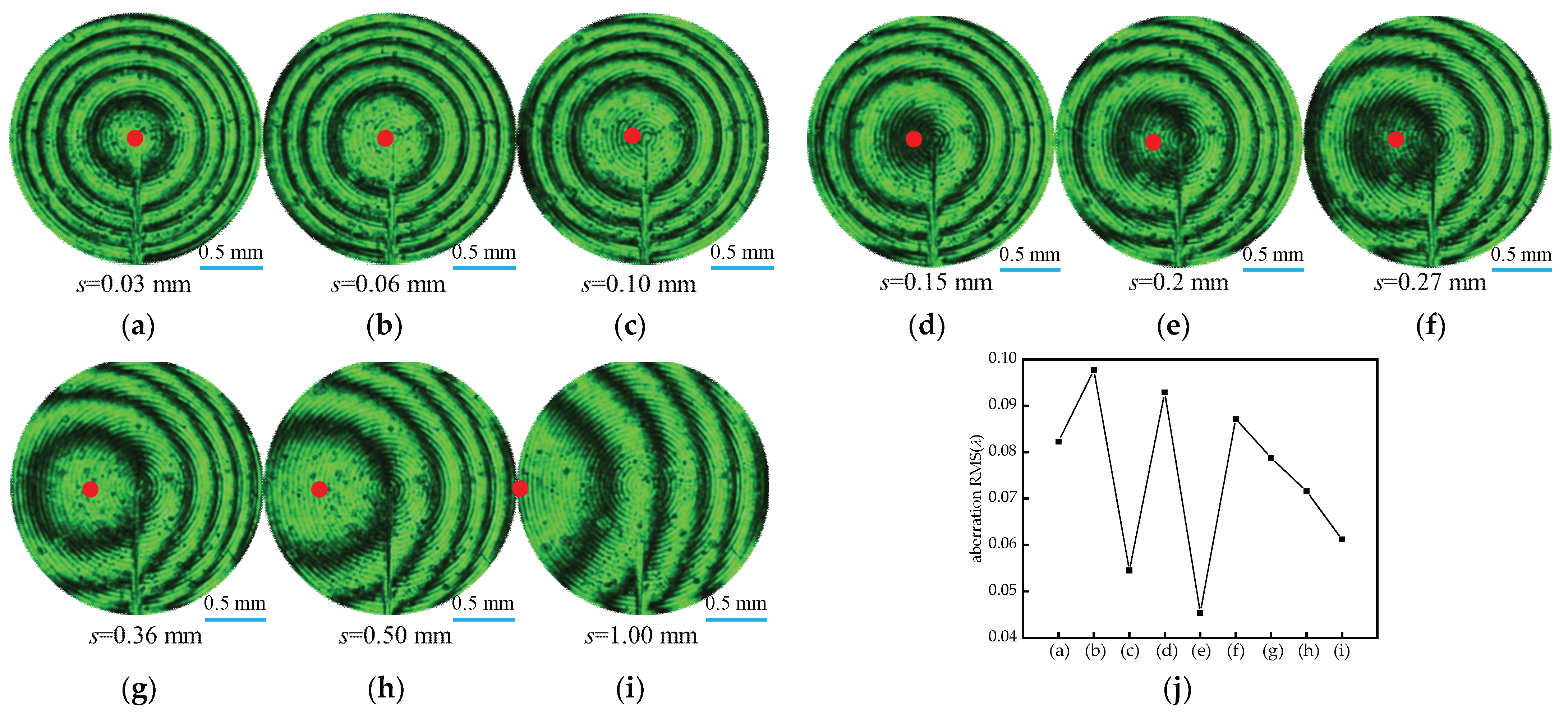
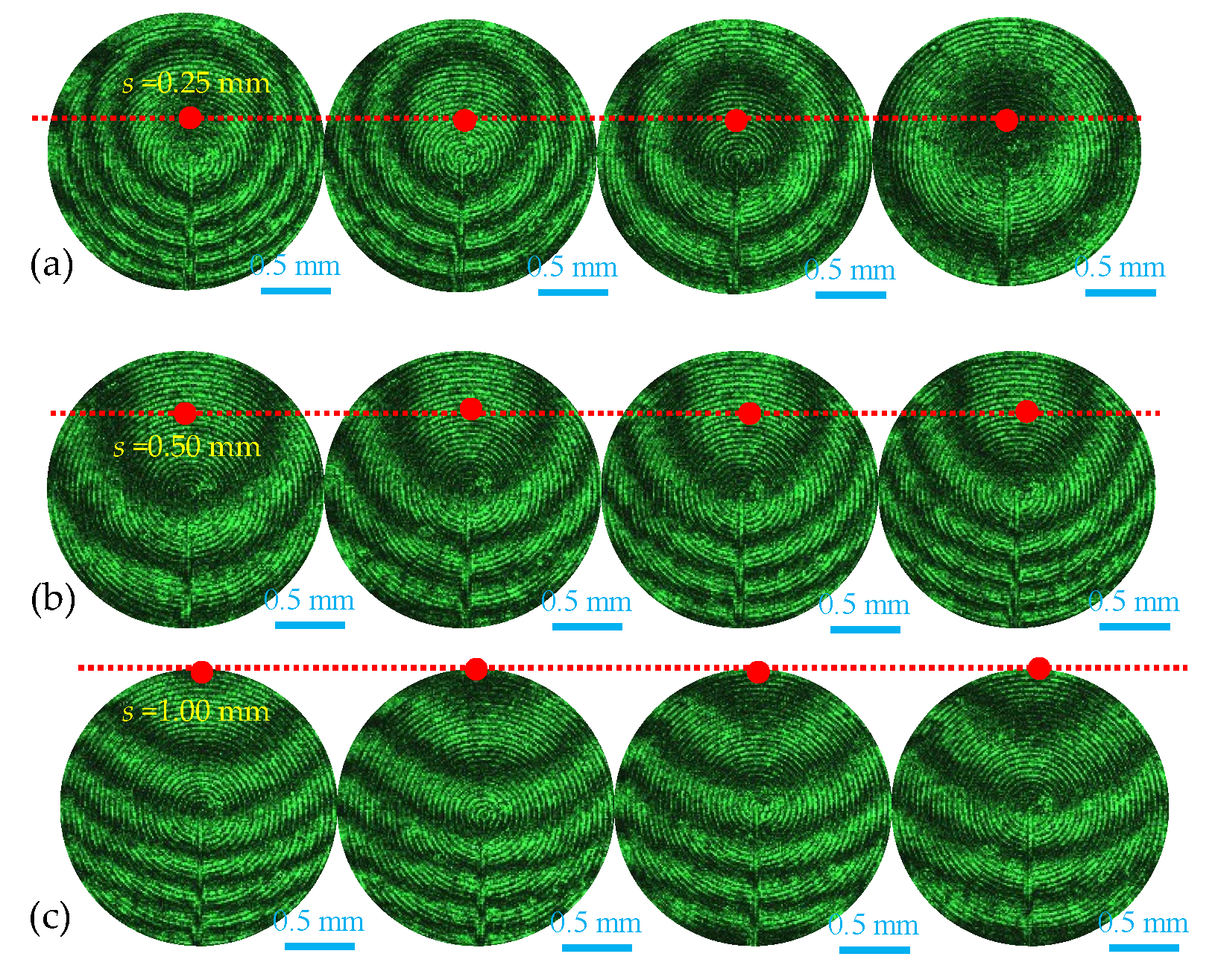
3.3.2. Fixed m, Gradual t, Fixed Focal Length OAM Lens with Equal Movement

Fixed m at 0.8, the maximum value of t was 0.8 from the Table 1. According to Equations (4) and (5), fixed m means fixed focal length and a gradual change in t means a gradual change in the movement of the OAM lens. s. t is gradually changed in increments of 0.2. These m and t are listed in Table 3. The interference fringes of the lens are measured by the setup in Figure 4. Accordingly, the interference fringes of the lens only exhibit movement in Figure 10a–e.

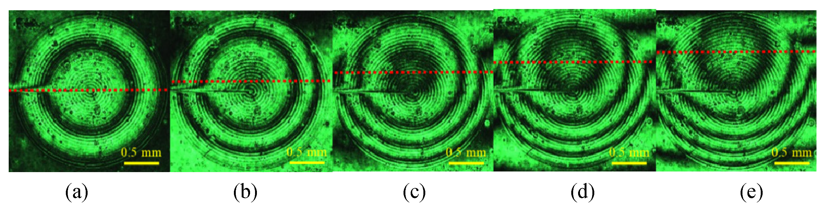
3.3.3. Changing m and t, Fixed OAM Lens with Changed Focal Length

According to Equations (4) and (5), if the optical axis of the OAM lens is to be fixed, both m and t should be adjusted simultaneously to ensure that the position of the optical axis s remains constant. In this part, three fixed optical axis OAMs were recorded in Figure 11. The movements of the OAM lens are s = 0.25 mm, s = 0.5 mm, and s = 1.00 mm. The concrete values of m and t are listed in Table 4
When the optical axis of the OAM lens is fixed, we can observe that the m and t increase simultaneously, which means the number of fringes within the aperture increases. The red dashed line refers to the position of the center of the lens. A series of fringes demonstrated that once the optical axis of the OAM lens is fixed away from the center, the changes in the m and t can only influence the focal length of the lens from Equation (5); it can achieve zoom at a position away from the center of the lens.

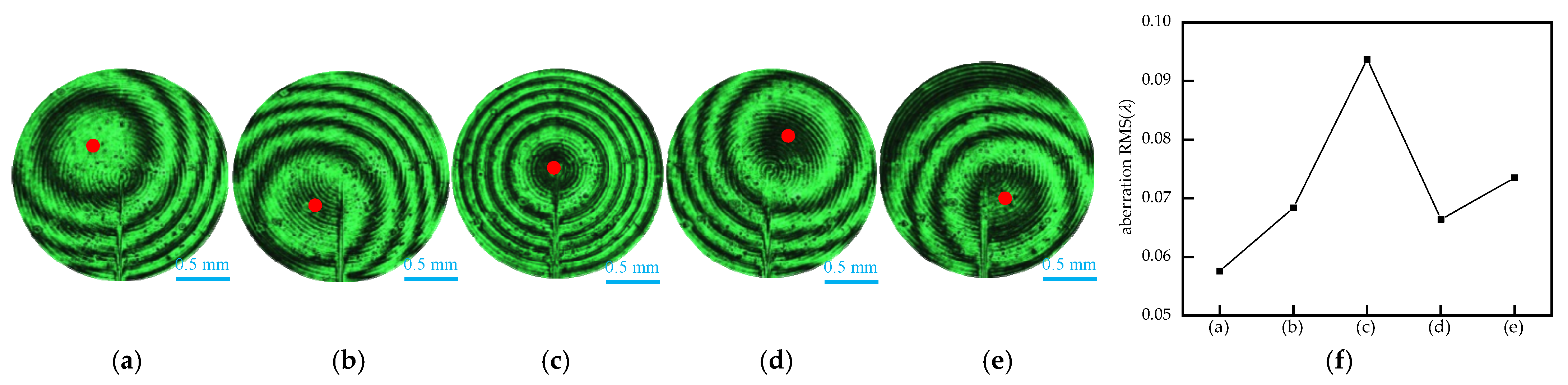
3.3.4. Fixed m and t, the OMA Lens Moves within the Aperture in Multiple Directions

Finally, we demonstrated the multi-directional movement of the OAM lens within the aperture. In order to record fringes clearly, the m and t are fixed at 1.0 and 0.6, respectively. The constant movement of the optical axis is s = 0.3 mm. The interference fringes are captured during the optical axis shift in Figure 12a–e.
Unlike the previous unidirectional movement, the applying voltage Va and p of the eight electrodes remained, but the applying positions needed to be changed. Assuming the driving voltage at the top left corner position is Vleftup, Vleftup was listed in Table 5. The total root-mean-square (RMS) errors of the wavefront are then extracted and are shown in Figure 12f. It can be seen that OAM lenses have a small RMS error during multi-directional movement.
In summary, through the selection of various m and t, we have verified the feasibility of equidistant OAM LC lenses, constant optical axis offset LC lenses, and arbitrary range OAM LC lenses. The theoretical movement amount was compared with the actual OAM, and the consistency of the two datasets verified the effectiveness of the simulation for the actual voltage application situation. The lens can be moved to infinity, which is the horizontal stripe. The maximum optical power is ±6D, and the minimum focal length is 16.7 cm.

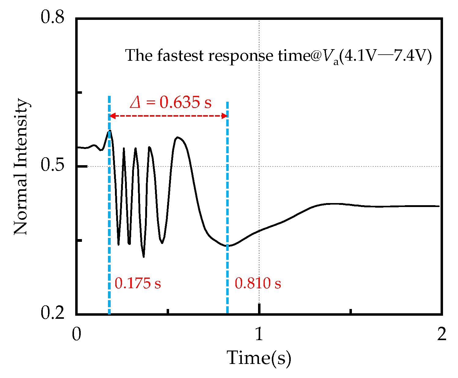
3.4. Phase Delay Response Time

When no phase difference is generated, the eight electrodes of the OAM lens can be applied with the same voltages at 0 V and 4.1 V, but under the condition of 0 V, the response time of the OAM lens is too long to take 2–3 s, which will limit its application. However, when applying the voltage at 4.1 V, the response time of the OAM lens is significantly shortened for the LC, which is driven by pre-voltage. In this paper, the thickness of the LC is 30 μm, and response times can reach 0.635 s in Figure 13, which is regularly 2–3 s [21].
The response time is measured based on the intensity changes during the variations of the fringes. The response time of the nematic LC lens is expressed as [41]
τ r = γ d 2 Δ ε ( V 2 V t h 2 )
γ: the visco-elastic coefficient, d: the thickness of the LC layer, V: driving voltage, Vth: threshold voltage. In practical applications, it is possible to use a low-viscosity LC material or reduce the thickness of the LC layer to increase the response speed. Moreover, the overdrive voltage method and undershoot effect can be used to reduce the response time [42].

4. Conclusions and Discussion

In conclusion, an LC lens with a movable optical axis is proposed and experimentally demonstrated firstly without mechanical movement. It can also function as a 3D wedge with a 0.164° steering angle. Experimentally, the vibration of the optical axis ranges from 0.164°, and the movement of the optical axis can reach infinity and remain unchanged during the movement, but there is a trade-off between movement and dioptre power of the OAM LC lens. In addition to the extremely shortened response time, it can be used for OIS. The comparison is listed in Table 6.
For an LC with normal dispersion, the refractive index difference Δn is a function of wavelength.
Δ n = n e n o = a + b λ 2 + c λ 4
a, b, and c are Cauchy dispersion coefficients related to the liquid crystal material. The maximum dioptre power (OPmax) of the LC lens can be expressed as
O P m a x = 2 d r 2 ( a + b λ 2 + c λ 4 )
It can be seen that even if the thickness of the LC layer, the size of the aperture, and the birefringence difference of the LC lens are determined, its dioptre power will still be affected by wavelength. When polychromatic light passes through the LC lens and becomes a converging/diverging spherical wave, it will still be affected by the chromatic dispersion of the LC layer. This causes the focal point of different wavelengths to be separated in different image planes, resulting in the difference in retardation at different wavelengths of the liquid crystal lens. This effect will become more severe as the thickness of the liquid crystal layer and the difference in the birefringence of the liquid crystal lens increase.

Supplementary Materials

The following supporting information can be downloaded at https://www.mdpi.com/article/10.3390/cryst14100843/s1; Video S1: OAM LC lens.

Author Contributions

Conceptualization, Q.W. and H.Z.; methodology, Q.W. and H.Z.; validation, Q.W., H.Z., D.J. and T.L.; investigation, Q.W.; data curation, Q.W., H.Z., D.J. and T.L.; writing—original draft preparation, Q.W.; writing—review and editing, H.Z., D.J. and T.L.; supervision, D.J. and T.L.; project administration, H.Z., D.J. and T.L. All authors have read and agreed to the published version of the manuscript.

Funding

This work was funded by the National Natural Science Foundation of China (42175097).

Institutional Review Board Statement

Not applicable.

Informed Consent Statement

Not applicable.

Data Availability Statement

Data are provided within the manuscript or Supplementary Information files. The author confirms that all data generated or analysed during this study are included in this published article. Furthermore, primary and secondary sources and data supporting the findings of this study were all publicly available at the time of submission.

Conflicts of Interest

The authors declare no conflicts of interest.

References

  1. Sun, M.; Feng, Y.; Wang, Y.; Huang, W.; Su, S. Design, Analysis and Experiment of a Bridge-Type Piezoelectric Actuator for Infrared Image Stabilization. Micromachines 2021, 12, 1197. [Google Scholar] [CrossRef] [PubMed]
  2. Bleier, B.J.; Yezer, B.A.; Freireich, B.J.; Anna, S.L.; Walker, L.M. Droplet-Based Characterization of Surfactant Efficacy in Colloidal Stabilization of Carbon Black in Nonpolar Solvents. J. Colloid Interface Sci. 2017, 493, 265–274. [Google Scholar] [CrossRef] [PubMed]
  3. Karasikov, N.; Peled, G.; Yasinov, R.; Feinstein, A. Piezo-Based, High Dynamic Range, Wide Bandwidth Steering System for Optical Applications; Pham, T., Kolodny, M.A., Eds.; SPIE: Anaheim, CA, USA, 2017; p. 101901C. [Google Scholar]
  4. Zheng, Y.; Fu, Y.G.; He, W.J.; Wang, J.K.; Zhang, L. Opto-Mechanical Structure Design of the Image Stabilization Collimator. Key Eng. Mater. 2013, 552, 79–84. [Google Scholar] [CrossRef]
  5. Meng, Z.; Huang, W.; Zhang, L.; Zhou, X.; Zhao, K.; Pu, D.; Chen, L. Large Aperture and Defect-Free Liquid Crystal Planar Optics Enabled by High-Throughput Pulsed Polarization Patterning. Opt. Express 2023, 31, 30435. [Google Scholar] [CrossRef]
  6. Yoshida, S.; Schmid, W.; Vo, N.; Calabrase, W.; Kisley, L. Computationally-Efficient Spatiotemporal Correlation Analysis Super-Resolves Anomalous Diffusion. Opt. Express 2021, 29, 7616. [Google Scholar] [CrossRef]
  7. Sun, Z.; Yuan, Z.; Nikita, A.; Kwok, H.; Srivastava, A.K. Fast-Switchable, High Diffraction-Efficiency Ferroelectric Liquid Crystal Fibonacci Grating. Opt. Express 2021, 29, 13978. [Google Scholar] [CrossRef]
  8. Cheng, K.; Li, Z.; Wu, J.; Hu, Z.-D.; Wang, J. Super-Resolution Imaging Based on Radially Polarized Beam Induced Superoscillation Using an All-Dielectric Metasurface. Opt. Express 2022, 30, 2780. [Google Scholar] [CrossRef]
  9. Chen, H.; Yu, S. A Stereo Camera Tracking Algorithm Used in Glass-Free Stereoscopic Display System. J. Comput. -Aided Des. Comput. Graph. 2017, 29, 436–443. [Google Scholar]
  10. Li, R.; Zhang, H.; Chu, F.; Wang, Q. Compact Integral Imaging 2D/3D Compatible Display Based on Liquid Crystal Micro-Lens Array. Liq. Cryst. 2022, 49, 512–522. [Google Scholar] [CrossRef]
  11. Dong, J.; Li, Z.; Liu, X.; Zhong, W.; Wang, G.; Liu, Q.; Song, X. High-Speed Real 3D Scene Acquisition and 3D Holographic Reconstruction System Based on Ultrafast Optical Axial Scanning. Opt. Express 2023, 31, 21721. [Google Scholar] [CrossRef]
  12. Juodkazis, S.; Shikata, M.; Takahashi, T.; Matsuo, S.; Misawa, H. Fast Optical Switching by a Laser-Manipulated Microdroplet of Liquid Crystal. Appl. Phys. Lett. 1999, 74, 3627–3629. [Google Scholar] [CrossRef]
  13. Kawamura, M.; Ye, M.; Sato, S. Optical Tweezers System by Using a Liquid Crystal Optical Device. Mol. Cryst. Liq. Cryst. 2007, 478, 135–891. [Google Scholar] [CrossRef]
  14. Wu, Q.; Zhang, H.; Jia, D.; Liu, T. Recent Development of Tunable Optical Devices Based on Liquid. Molecules 2022, 27, 8025. [Google Scholar] [CrossRef] [PubMed]
  15. Maksymova, I.; Greiner, P.; Wiesmeier, J.; Darrer, F.M.; Druml, N. A MEMS Mirror Driver ASIC for Beam-Steering in Scanning MEMS-Based LiDAR. In Proceedings of the Laser Beam Shaping XIX, San Diego, CA, USA, 11–12 August 2019; Dudley, A., Laskin, A.V., Eds.; SPIE: San Diego, CA, USA, 2019; p. 11. [Google Scholar]
  16. Galaktionov, I.; Kudryashov, A.; Sheldakova, J.; Nikitin, A. Laser Beam Focusing through the Dense Multiple Scattering Suspension Using Bimorph Mirror. In Proceedings of the Adaptive Optics and Wavefront Control for Biological Systems V, San Diego, CA, USA, 3–4 February 2019; Bifano, T.G., Gigan, S., Ji, N., Eds.; SPIE: San Francisco, CA, USA, 2019; p. 44. [Google Scholar]
  17. Wlodarczyk, K.L.; Bryce, E.; Schwartz, N.; Strachan, M.; Hutson, D.; Maier, R.R.J.; Atkinson, D.; Beard, S.; Baillie, T.; Parr-Burman, P.; et al. Scalable Stacked Array Piezoelectric Deformable Mirror for Astronomy and Laser Processing Applications. Rev. Sci. Instrum. 2014, 85, 024502. [Google Scholar] [CrossRef]
  18. Verpoort, S.; Wittrock, U. Unimorph Deformable Mirror for Telescopes and Laser Applications. In Proceedings of the International Conference on Space Optics—ICSO 2010, Rhodes Island, Greece, 4–8 October 2010; Armandillo, E., Cugny, B., Karafolas, N., Eds.; SPIE: Rhodes Island, Greece, 2019; p. 527. [Google Scholar]
  19. Salter, P.S.; Booth, M.J. Adaptive Optics in Laser Processing. Light Sci. Appl. 2019, 8, 10. [Google Scholar] [CrossRef]
  20. Nose, T.; Sato, S. A Liquid Crystal Microlens Obtained with a Non-Uniform Electric Field. Liq. Cryst. 1989, 5, 1425–1433. [Google Scholar] [CrossRef]
  21. Morris, R.; Jones, C.; Nagaraj, M. Liquid Crystal Devices for Beam Steering Applications. Micromachines 2021, 12, 247. [Google Scholar] [CrossRef]
  22. He, Z.; Gou, F.; Chen, R.; Yin, K.; Zhan, T.; Wu, S.-T. Liquid Crystal Beam Steering Devices: Principles, Recent Advances, and Future Developments. Crystals 2019, 9, 292. [Google Scholar] [CrossRef]
  23. Sato, S. Applications of Liquid Crystals to Variable-Focusing Lenses. Opt. Rev. 1999, 6, 471–485. [Google Scholar] [CrossRef]
  24. Reshetnyak, V.Y.; Sova, O.; Wang, Y.-J.; Lin, Y.-H. Modeling Liquid Crystal Lenses. In Proceedings of the Emerging Liquid Crystal Technologies XV, San Diego, CA, USA, 3–5 February 2020; Chien, L.-C., Broer, D.J., Eds.; SPIE: San Francisco, CA, USA, 2020; p. 3. [Google Scholar]
  25. Love, G.D.; Major, J.V.; Purvis, A. Liquid-Crystal Prisms for Tip-Tilt Adaptive Optics. Opt. Lett. 1994, 19, 1170. [Google Scholar] [CrossRef]
  26. Hands, P.J.W.; Tatarkova, S.A.; Kirby, A.K.; Love, G.D. Modal Liquid Crystal Devices in Optical Tweezing: 3D Control and Oscillating Potential Wells. Opt. Express 2006, 14, 4525. [Google Scholar] [CrossRef] [PubMed]
  27. Kotova, S.P.; Patlan, V.V.; Samagin, S.A. Tunable Liquid-Crystal Focusing Device. 2. Experiment. Quantum Electron. 2011, 41, 65–70. [Google Scholar] [CrossRef]
  28. Xu, L.; Zhang, Y.; Liu, Z.; Ye, M. Driving Method for Adjustable Liquid Crystal Optical Wedge with Four Electrodes. Acta Opt. Sin. 2022, 42, 1323001. [Google Scholar] [CrossRef]
  29. Ye, M.; Sato, S. Liquid Crystal Lens with Focus Movable along and off Axis. Opt. Commun. 2003, 225, 277–280. [Google Scholar] [CrossRef]
  30. Ye, M.; Wang, B.; Sato, S. Liquid Crystal Lens with Focus Movable in Focal Plane. Opt. Commun. 2006, 259, 710–722. [Google Scholar] [CrossRef]
  31. Ye, M.; Wang, B.; Uchida, M.; Yanase, S.; Takahashi, S.; Yamaguchi, M.; Sato, S. Low-Voltage-Driving Liquid Crystal Lens. Jpn. J. Appl. Phys. 2010, 49, 100204. [Google Scholar] [CrossRef]
  32. Bennis, N.; Jankowski, T.; Strzezysz, O.; Pakuła, A.; Zografopoulos, D.C.; Perkowski, P.; Sánchez-Pena, J.M.; López-Higuera, J.M.; Algorri, J.F. A High Birefringence Liquid Crystal for Lenses with Large Aperture. Sci. Rep. 2022, 12, 14603. [Google Scholar] [CrossRef]
  33. Bennis, N.; Jankowski, T.; Morawiak, P.; Spadlo, A.; Zografopoulos, D.C.; Sánchez-Pena, J.M.; López-Higuera, J.M.; Algorri, J.F. Aspherical Liquid Crystal Lenses Based on a Variable Transmission Electrode. Opt. Express 2022, 30, 12237. [Google Scholar] [CrossRef]
  34. Algorri, J.F.; Love, G.D.; Urruchi, V. Modal Liquid Crystal Array of Optical Elements. Opt. Express 2013, 21, 24809. [Google Scholar] [CrossRef]
  35. Algorri, J.F.; Morawiak, P.; Zografopoulos, D.C.; Bennis, N.; Spadlo, A.; Rodríguez-Cobo, L.; Jaroszewicz, L.R.; Sánchez-Pena, J.M.; López-Higuera, J.M. Multifunctional Light Beam Control Device by Stimuli-Responsive Liquid Crystal Micro-Grating Structures. Sci. Rep. 2020, 10, 13806. [Google Scholar] [CrossRef]
  36. Algorri, J.F.; Morawiak, P.; Bennis, N.; Zografopoulos, D.C.; Urruchi, V.; Rodríguez-Cobo, L.; Jaroszewicz, L.R.; Sánchez-Pena, J.M.; López-Higuera, J.M. Positive-Negative Tunable Liquid Crystal Lenses Based on a Microstructured Transmission Line. Sci. Rep. 2020, 10, 10153. [Google Scholar] [CrossRef] [PubMed]
  37. Feng, W.; Liu, Z.; Liu, H.; Ye, M. Design of Tunable Liquid Crystal Lenses with a Parabolic Phase Profile. Crystals 2022, 13, 8. [Google Scholar] [CrossRef]
  38. Cao, F.; Liu, Z.; Ye, M. Modulated Beam Deflection by Liquid Crystal Optical Wedge Arrays. Acta Opt. Sin. 2024, 44, 251–257. [Google Scholar] [CrossRef]
  39. Elston, S.J. Optics and Nonlinear Optics of Liquid Crystals. J. Mod. Opt. 1994, 41, 1517–1518. [Google Scholar] [CrossRef]
  40. Feng, W.; Liu, Z.; Ye, M. Positive-Negative Tunable Cylindrical Liquid Crystal Lenses. Optik 2022, 266, 169613. [Google Scholar] [CrossRef]
  41. Xu, S.; Li, Y.; Liu, Y.; Sun, J.; Ren, H.; Wu, S.-T. Fast-Response Liquid Crystal Microlens. Micromachines 2014, 5, 300–324. [Google Scholar] [CrossRef]
  42. Yang, D.-K.; Wu, S.-T. Fundamentals of Liquid Crystal Devices; John Wiley & Sons: Hoboken, NJ, USA, 2014. [Google Scholar] [CrossRef]
Figure 1. (a) 3D structure diagram of the device, (b) top electrode with electrode wire and gap are both 10 um; (c) bottom electrode, (d) movement of OAM LC lens focus, (e) focus moving area in 3D space (The color represents the focal length).
Crystals 14 00843 g001
Figure 2. (a) The whole region with Va is the minimum input voltage of the eight copper electrodes; p is the voltage increment in the X direction; (b) the core region of the bottom electrode; the color bars in (a,b) are used to display the voltage within the area (c) the voltage difference between the top and bottom electrode. the black line represents the top layer voltage distribution, the red line represents the bottom layer voltage distribution, and the green dashed line represents the voltage difference between the upper and lower electrodes; (d) the variation in center voltage with the sheet resistance (εr) ratio, the red and blue lines respectively represent the sheet resistance ratio and voltage value when the voltage is exactly stable.
Crystals 14 00843 g002
Figure 3. (a) Schematic of image shift caused by optical axis vibration and OAM lens eliminate the shift (the black line represents the light path, while the red line represents the movement of the lens); (b) extracted phase delay of the LC layer and the linear response range of the LC material, the black line represents the response of the LC, and the red dashed line represents the linear response region of the LC; (c) the red line is the trade-off between m and t, blue line represents the range of the m and t.
Crystals 14 00843 g003
Figure 4. Orthogonal interference setup to capture the fringes.
Crystals 14 00843 g004
Figure 5. Image movement observation experimental setup, the prepared LC lens, and wire leads. The resolution panel is attached on the box for fixation.
Crystals 14 00843 g005
Figure 6. (af) The 3D spatial light deflection effect of the LC wedge; (g) the relationship between the azimuth angle of the LC wedge and the voltage distribution on both sides.
Crystals 14 00843 g006
Figure 7. Camera imaging position shift under LC wedge: center image (a), up shift (b), lower shift (c), left shift (d), right shift (e), up left (f), up right (g), lower left (h), lower right (i). Red and yellow lines are observation aids; the blue box ‘2’ indicates horizontal movement comparison, and the black box ‘9’ indicates vertical movement comparison (j) movement of figures.
Crystals 14 00843 g007
Figure 8. The trade-off between movement and dioptre power of the OAM lens.
Crystals 14 00843 g008
Figure 9. Interference fringes of OAM LC lens when m and t are within critical condition (a) t = 0.1; (b) t = 0.2; (c) t = 0.3; (d) t = 0.4; (e) t = 0.5; (f) t = 0.6; (g) t = 0.7; (h) t = 0.8; (i) t = 0.9, (j) the aberration RMS error, and the red dot is the center of the lens.
Crystals 14 00843 g009aCrystals 14 00843 g009b
Figure 10. The interOAM lens in one direction with different movements: (a) initial state; (b) 0.125 mm movement; (c) 0.25 mm movement; (d) 0.375 mm movement; (e) 0.5 mm movement. The red line shows the vertical movement of the lens.
Crystals 14 00843 g010
Figure 11. Interference fringes of the OAM lens with a fixed optical axis that represents the following s fixed movements: (a) 0.25 mm; (b) 0.5 mm; (c) 1.00 mm of the OAM lens. The red dot is the center of the lens and the red line shows the vertical movement of the lens.
Crystals 14 00843 g011
Figure 12. Interference fringes of the LC lens when the optical axis is shifted to different positions. (ae) multiple directions, (f) the total RMS aberration of the OAM lens. The red dot is the center of the lens.
Crystals 14 00843 g012
Figure 13. Response time of LC from initial state to maximum working state. The blue lines represent the start and end of the response time, respectively. The response time is 0.635 s.
Crystals 14 00843 g013
Table 1. The driving voltage and parameter of the different azimuth angle.
(a)(b)(c)(d)(e)(f)
Va0.8 V0.8 V0.8 V0.8 V0.8 V0.8 V
p1.1 V2.23.34.45.56.6
θa77.661.343.826.310.60
θw0.17°0.17°0.17°0.17°0.17°0.17°
Table 2. m and t at the critical condition.
m (V·mm−2)t (V·mm−1)s (mm)Sfigure (mm)Va (V)
1.700.100.0290.033.73
1.590.200.0630.073.37
1.480.300.1010.113.00
1.370.400.1460.162.63
1.250.500.2000.222.27
1.120.600.2680.271.90
0.970.700.3610.381.53
0.450.800.5000.521.17
0.450.901.0000.980.80
Table 3. The driving voltage and parameter of the OAM.
(a)(b)(c)(d)(e)
Vmin (V)7.37.57.77.98.1
Vmax (V)8.18.38.58.78.9
m (V·mm−2)0.80.80.80.80.8
t (V·mm−1)00.20.40.17°0.17°
s (mm)00.1250.2500.3750.500
Sfigure (mm)00.1260.2513.7800.495
Table 4. The driving voltage and parameter of the fixed optical axis.
s (mm)m (V·mm−2)t (V·mm−1)Va (V)
0.250.400.203.37
0.600.303.00
0.800.402.63
1.000.502.27
0.500.400.402.63
0.500.502.27
0.600.601.90
0.700.701.53
1.000.300.601.90
0.350.701.53
0.400.801.17
0.450.900.80
Table 5. The driving voltage and parameter of optical axis multi-directional movement.
m (V·mm−2)t (V·mm−1)s (mm)Vleftup (V)p (V)Azimuth Angle
1.00.600.301.902.2045° (left up)
1.00.600.304.102.2045° (left down)
1.00.600.304.100
1.00.600.304.102.2045° (right up)
1.00.600.301.902.2045° (right down)
Table 6. Works compared with other typical papers.
LC DevicesBeam DeflectorsOAM LensResponse Time
AngleDimensionThicknessMovementDimensionAberration
Hands [26]0.024°3D50 μm2–3 s
Ye [13]0.1°2D130 μm
J.F.Algorri [35]0.008°2D50 μm
Feng [37]50 μm1.0 mm1D < 0.1   λ 2–3 s
This paper0.164°3D30 μm0~∞ (firstly)2D < 0.1   λ 0.635–3 s
Disclaimer/Publisher’s Note: The statements, opinions and data contained in all publications are solely those of the individual author(s) and contributor(s) and not of MDPI and/or the editor(s). MDPI and/or the editor(s) disclaim responsibility for any injury to people or property resulting from any ideas, methods, instructions or products referred to in the content.

