
AlGaN-Based Ultraviolet PIN Photodetector Grown on Silicon Substrates Using SiN Nitridation Process and Step-Graded Buffers

 and
and 
Abstract
1. Introduction
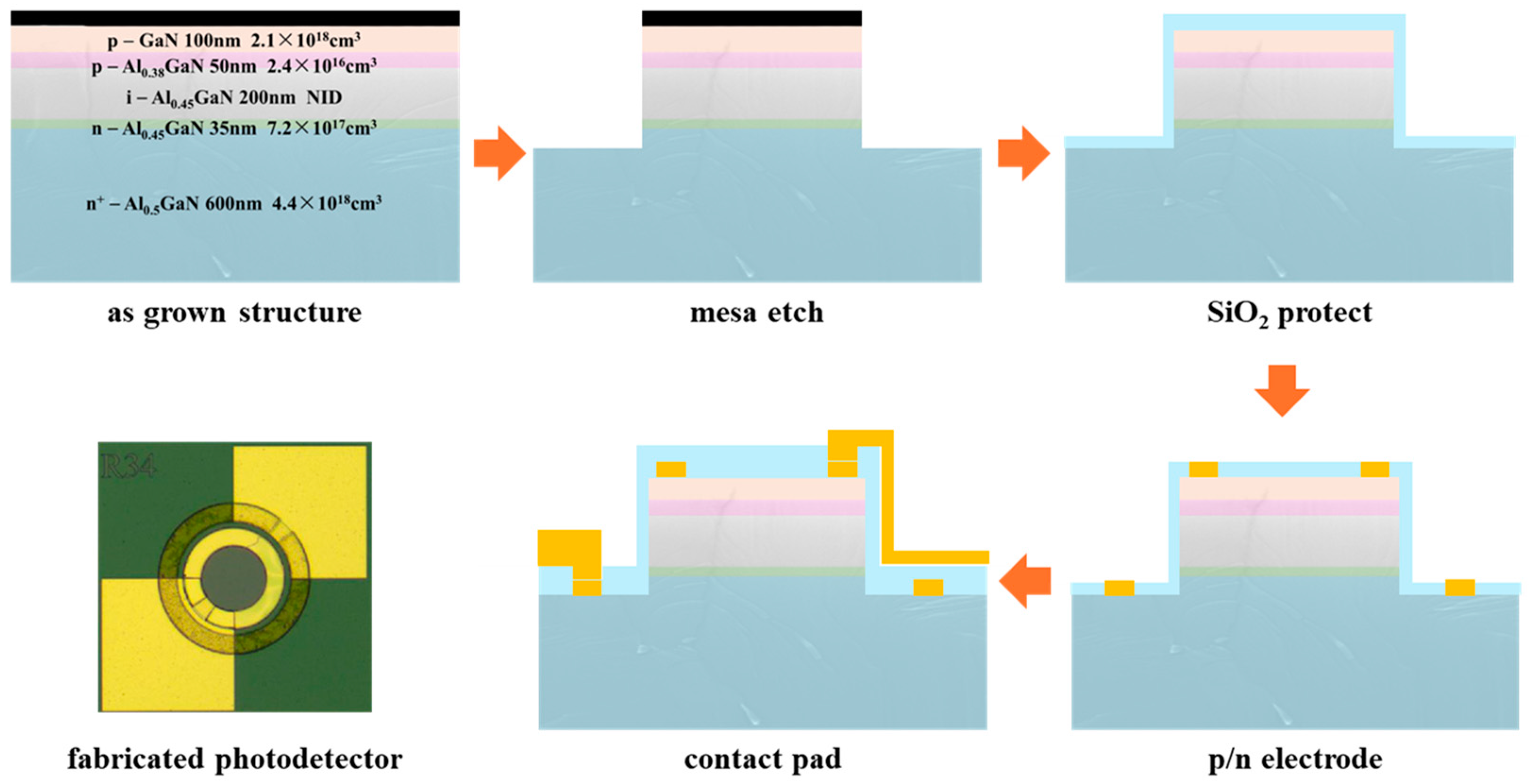
2. Materials and Methods
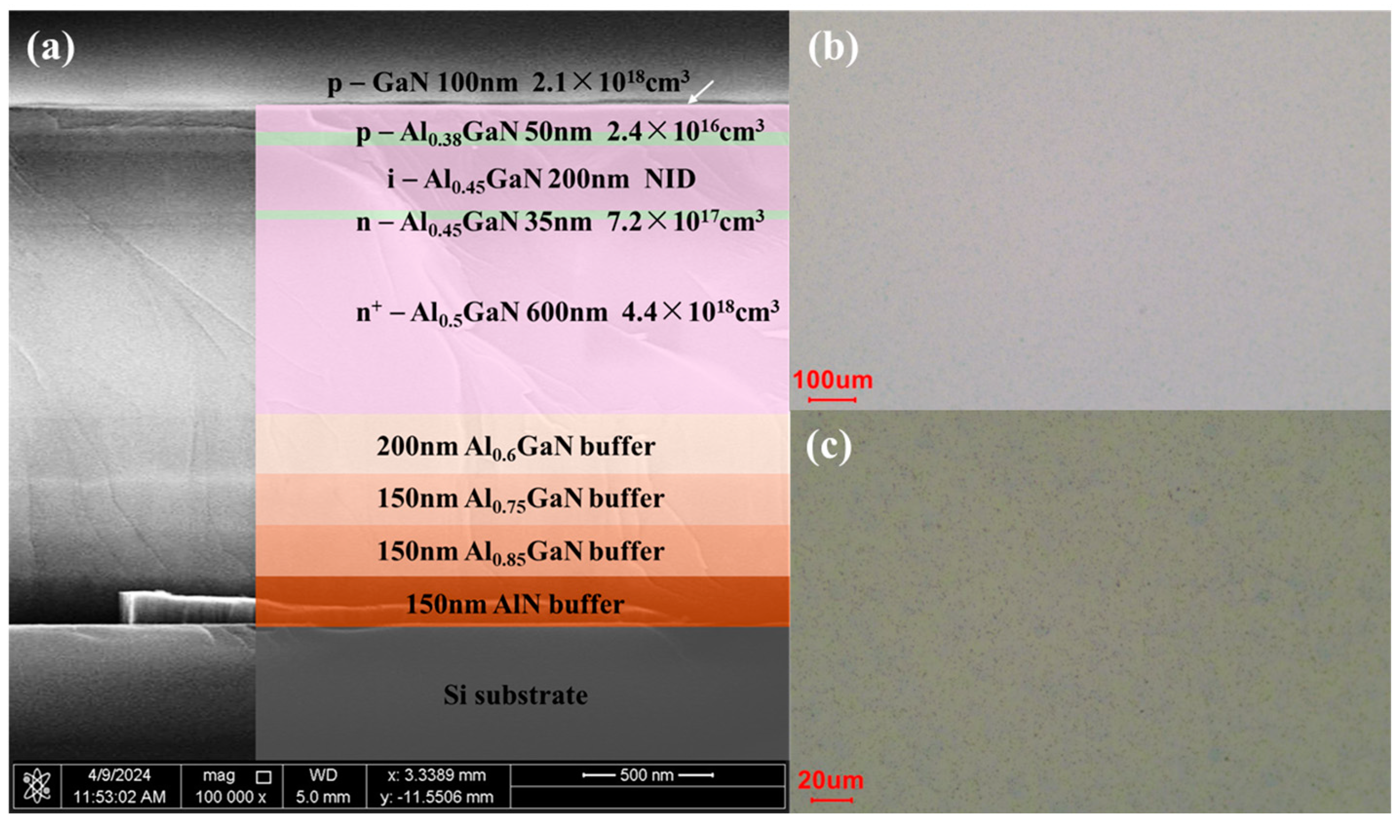
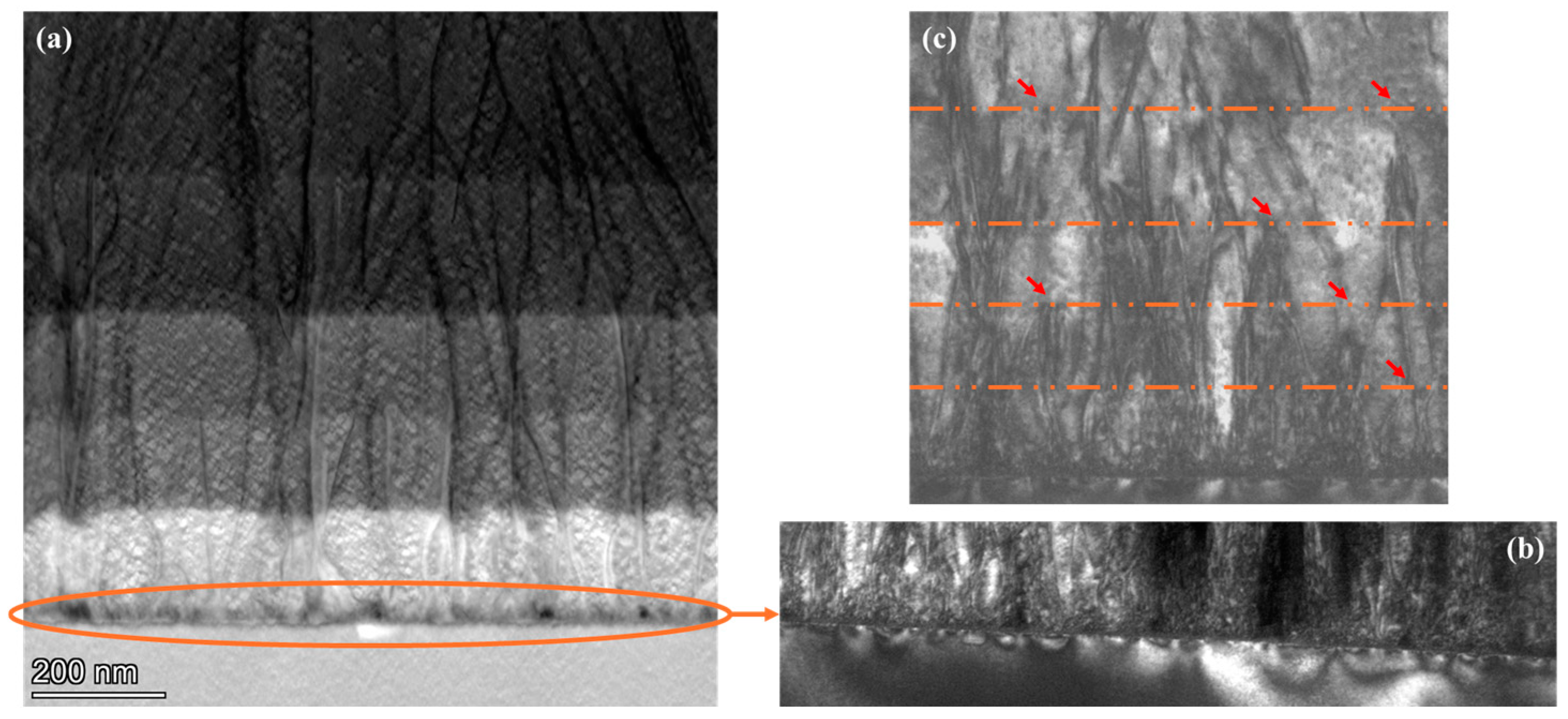
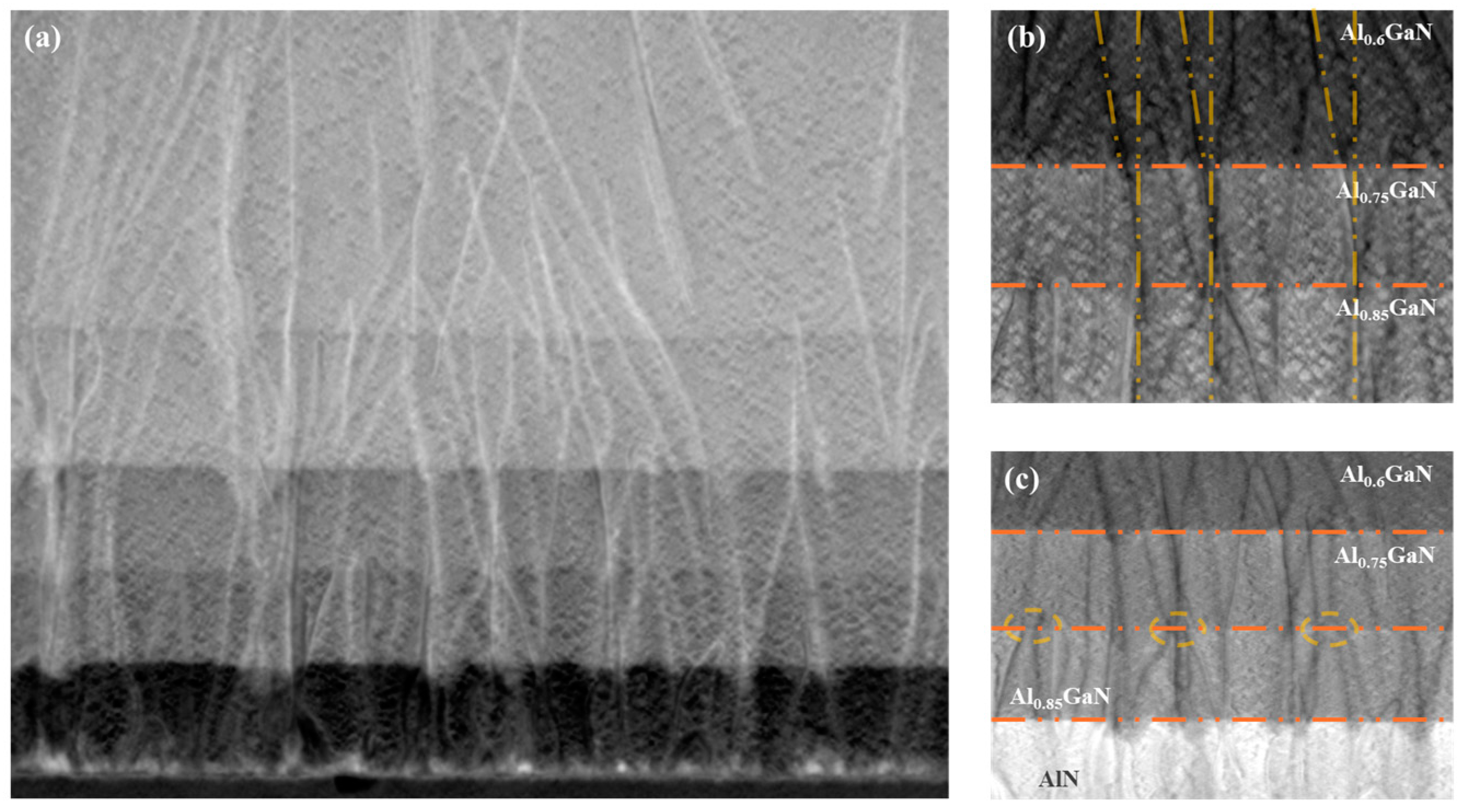
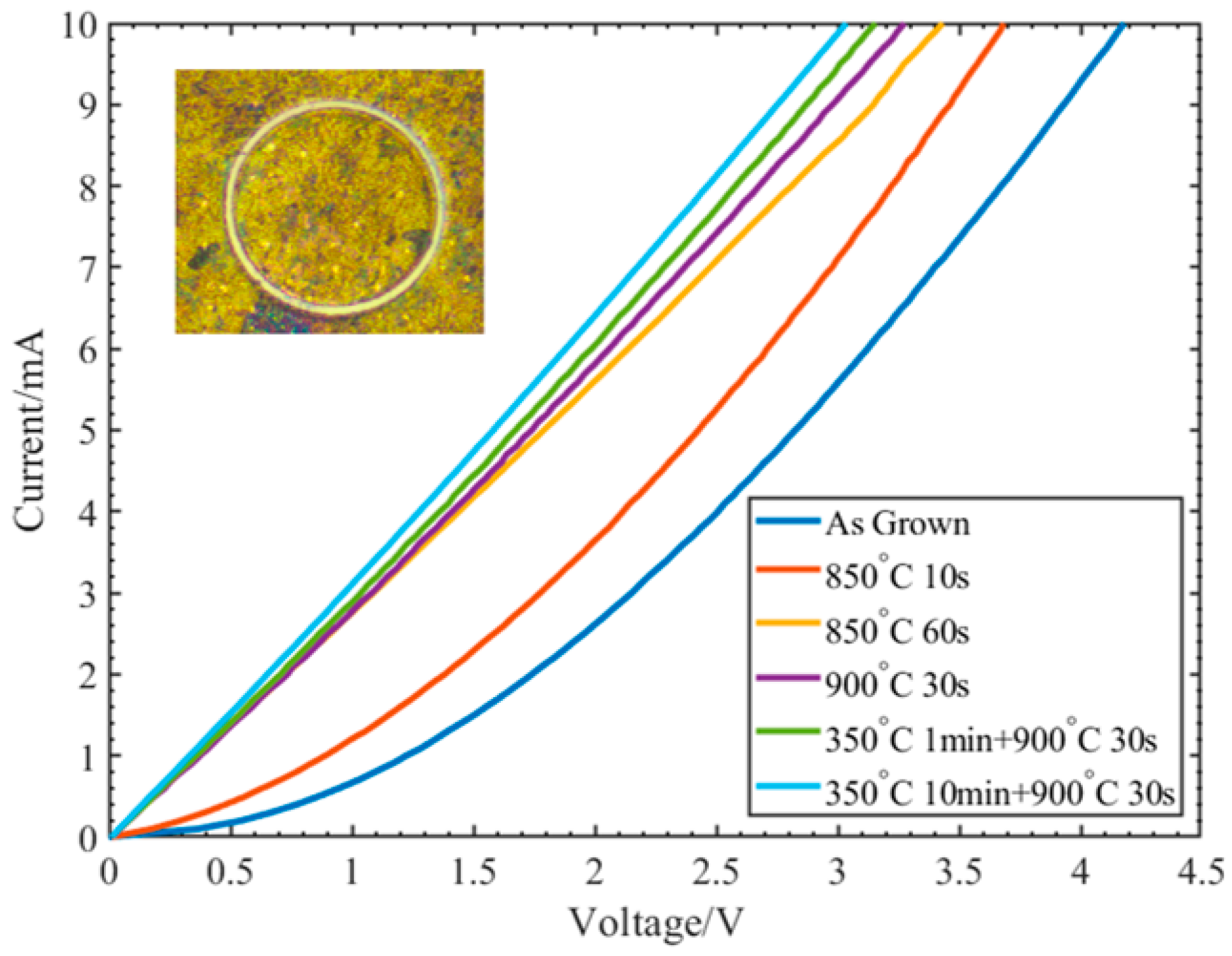
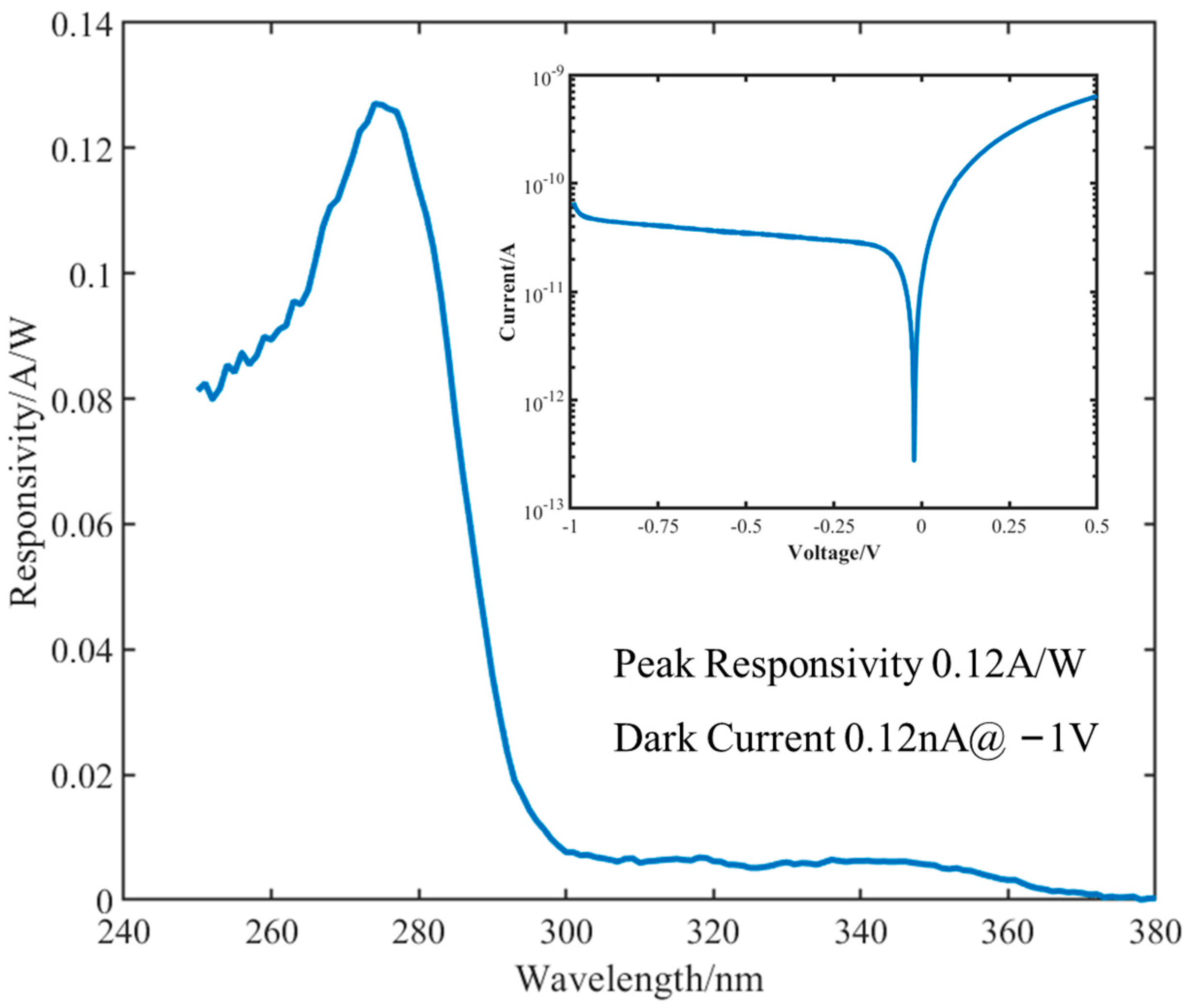
3. Results and Discussion
4. Conclusions
Author Contributions
Funding
Data Availability Statement
Acknowledgments
Conflicts of Interest
References
- Razeghi, M.; Rogalski, A. Semiconductor ultraviolet detectors. J. Appl. Phys. 1996, 79, 7433–7473. [Google Scholar] [CrossRef]
- Razeghi, M. Short-wavelength solar-blind detectors-status, prospects, and markets. Proc. IEEE 2002, 90, 1006–1014. [Google Scholar] [CrossRef]
- Patrick, K.; Alireza, Y.; Ryan, M.; Shaban, D.; Kan, M.; Manijeh, R. Future of AlxGa1-xN materials and device technology for ultraviolet photodetectors. Proc. SPIE 2002, 4650, 199–206. [Google Scholar] [CrossRef]
- Kamiyama, S.; Amano, H.; Akasaki, I. The Evolution of Nitride Semiconductors, Optoelectronic Devices: III Nitrides; Elsevier: Oxford, UK, 2005; Chapter 3; pp. 23–38. [Google Scholar] [CrossRef]
- Cicek, E.; McClintock, R.; Cho, C.Y.; Rahnema, B.; Razeghi, M. AlxGa1-xN-based back-illuminated solar-blind photodetectors with external quantum efficiency of 89%. Appl. Phys. Lett. 2013, 103, 191108. [Google Scholar] [CrossRef]
- Cicek, E.; Vashaei, Z.; Huang, E.K.; McClintock, R.; Razeghi, M. AlGaN-based deep ultraviolet 320×256 focal plane array. Opt. Lett. 2012, 37, 896–898. [Google Scholar] [CrossRef]
- Wang, G.S.; Lu, H.; Xie, F.; Chen, D.J.; Ren, F.F.; Zhang, R.; Zheng, Y.D. High quantum efficiency back-illuminated AlGaN based solar-blind ultraviolet pin photodetectors. Chin. Phys. Lett. 2012, 29, 097302. [Google Scholar] [CrossRef]
- Yuan, Y.G.; Zhang, Y.; Chu, K.H.; Li, X.Y.; Li, X.Y.; Zhao, D.G.; Yang, H. Development of solar-blind AlGaN 128×128 ultraviolet focal plane arrays. Sci. China Ser. E-Technol. Sci. 2008, 51, 820–826. [Google Scholar] [CrossRef]
- Reverchon, J.L.; Bansropun, S.; Truffer, J.P.; Costard, E.; Frayssinet, E.; Brault, J.; Duboz, J.Y.; Giuliani, A.; Idir, M. Performances of AlGaN based focal plane arrays form 10 nm to 200 nm. In Space Missions and Technologies, Proceedings of SPIE—The International Society for Optical Engineering, Orlando, FL, USA, 7 May 2010; SPIE: Bellingham, WA, USA, 2010; Volume 7691, p. 769109. [Google Scholar] [CrossRef]
- Kumar, M.; Lee, C.Y.; Sekiguchi, H.; Okada, H.; Wakahara, A. Demonstration of a large area AlGaN/GaN Schottky barrier photodetector on Si with high detection limit. Semicond. Sci. Technol. 2013, 28, 094005. [Google Scholar] [CrossRef]
- Varshney, U.; Affarwal, N.; Gupta, G. Current advances in solar-blind photodetection technology: Using Ga2O3 and AlGaN. J. Mater. Chem. C 2022, 10, 1573–1593. [Google Scholar] [CrossRef]
- Cai, Q.; You, H.F.; Guo, H.; Wang, J.; Liu, B.; Xie, Z.L.; Chen, D.J.; Lu, H.; Zheng, Y.D.; Zhang, R. Progress on AlGaN based solar-blind ultraviolet photodetectors and focal plane arrays. Light Sci. Appl. 2021, 10, 94. [Google Scholar] [CrossRef]
- Gu, Y.; Guo, J.; Ye, B.; Yang, X.; Xie, F.; Qian, W.; Zhang, X.; Lu, N.; Liu, Y.; Yang, G. Self-powered AlGaN-based MSM solar-blind ultraviolet photodetectors with high Al-content AlxGa1-xN/AlyGa1-yN asymmetrical heterostructure. Appl. Phys. Lett. 2023, 123, 232103. [Google Scholar] [CrossRef]
- Zhang, N.H.; Wang, X.L.; Zeng, Y.P.; Xiao, H.L.; Wang, J.X.; Liu, H.X.; Li, J.M. Growth and properties of GaN on Si (111) substrates with AlGaN/AlN buffer layer by NH3-GSMBE. J. Phys. D: Appl. Phys. 2005, 38, 1888–1891. [Google Scholar] [CrossRef]
- Nikishin, S.A.; Faleev, N.N.; Antipov, V.G.; Francoeur, S.; De Peralta, L.G.; Seryogin, G.A.; Temkin, H.; Prokofyeva, T.I.; Holtz, M.; Chu, S.N.G. High quality GaN grown on Si (111) by gas source molecular beam epitaxy with ammonia. Appl. Phys. Lett. 1999, 75, 2073–2075. [Google Scholar] [CrossRef]
- Malin, T.; Maidebura, Y.; Mansurov, V.; Gavrilova, T.; Gutakovsky, A.; Vdovin, V.; Ponomarev, S.; Loshkarev, I.; Osinnykh, I.; Volodin, V.; et al. Influence of substrate nitridation conditions and buffer layer structures on the crack free GaN layers on Silicon substrate grown by ammonia-assisted molecular beam epitaxy. Thin Solid Films 2024, 791, 140246. [Google Scholar] [CrossRef]
- Milakhin, D.; Malin, T.; Mansurov, V.; Maidebura, Y.; Bashkatov, D.; Milekhin, I.; Goryainov, S.; Volodin, V.; Loshkarev, I.; Vdovin, V.; et al. Tackling residual tensile stress in AlN on Si nucleation layers via the controlled Si(111) surface nitridation. Surf. Interfaces 2024, 51, 104817. [Google Scholar] [CrossRef]
- Gkanatsiou, A.; Lioutas, C.B.; Frangis, N.; Polychroniadis, E.K.; Prystawko, P.; Leszczynski, M. Electron microscopy characterization of AlGaN/GaN heterostructures grown on Si (111) substrates. Superlattices Microstruct. 2017, 103, 376–385. [Google Scholar] [CrossRef]
- Ghosh, S.; Hinz, A.M.; Frentrup, M.; Alam, S.; Wallis, D.J.; Oliver, R.A. Design of step graded AlGaN buffer for GaN on Si heterostructures grown by MOCVD. Semicond. Sci. Technol. 2023, 38, 044001. [Google Scholar] [CrossRef]
- Sun, H.; Woodward, J.; Yin, J.; Moldawer, A.; Pecora, E.F.; Nikiforov, A.Y.; Negro, L.D.; Paiella, R.; Ludwig, K.; Smith, D.J.; et al. Development of AlGaN-based graded-index-separate-confinement-heterostructure deep UV emitters by molecular beam epitaxy. J. Vac. Sci. Technol. B 2013, 31, 03C117. [Google Scholar] [CrossRef]
- Carneiro, E.; Rennesson, S.; Tamariz, S.; Harrouche, K.; Semond, F.; Medjdoub, F. Submicrometer-thick setp-graded AlGaN buffer on Silicon with a high buffer breakdown field. Phys. Status Solidi A 2023, 220, 2200846. [Google Scholar] [CrossRef]
- Wang, T.; Liu, S.; Zheng, X.; Wang, P.; Wang, D.; Chen, Z.; Wei, J.; Rong, X.; Tao, R.; Guo, S.; et al. Microstructure and dislocation evolution in composition gradient AlGaN grown by MOCVD. Superlattices Microstruct. 2021, 152, 106842. [Google Scholar] [CrossRef]
- Kung, P.; Walker, D.; Hamilton, M.; Diaz, J.; Razeghi, M. Lateral epitaxial overgrowth of GaN films on sapphire and silicon substrates. Appl. Phys. Lett. 1999, 74, 570–572. [Google Scholar] [CrossRef]
- Mansurov, V.; Malin, T.; Galitsyn, Y.; Zhuravlev, K. Graphene-like AlN layer formation on (111) Si surface by ammonia molecular beam epitaxy. J. Cryst. Growth 2015, 428, 93–97. [Google Scholar] [CrossRef]
- Mansruov, V.G.; Galitsyn, Y.G.; Malin, T.V.; Teys, S.A.; Fedosenko, E.V.; Kozhukhov, A.S.; Zhuravlev, K.S.; Cora, I.; Pecz, B. Formation of a graphene-like SiN layer on the surface Si (111). Semiconductor 2018, 52, 1511–1517. [Google Scholar] [CrossRef]
- Zhuravlev, K.S.; Mansurov, V.; Galitsyn, Y.; Malin, T.; Milakhin, D.; Zemlyakov, V. Evolution of the surface states during the in situ SiN layer formation on AlN/GaN heterostrucutres. Semicond. Sci. Technol. 2020, 35, 075004. [Google Scholar] [CrossRef]
- Ishizaka, A.; Shiraki, Y. Low temperature surface cleaning of silicon and its application to silicon MBE. J. Electrochem. Soc. 1986, 133, 666–671. [Google Scholar] [CrossRef]
- Kern, W.; Puotinen, D.A. Cleaning solutions based on hydrogen peroxide for use in silicon semiconductor technology. RCA Rev. 1970, 31, 187–206. [Google Scholar]
- Mansurov, V.; Xu, X.Y.; Pandikunta, M.; Uddin, R.; Nikishin, S. Reflection high energy electron diffraction investigation and comparison of the initial stage during molecular beam epitaxy of AlN on Si (111) and Si(110) substrates. J. Vac. Sci. Technol. B 2011, 29, 03C129. [Google Scholar] [CrossRef]
- Tamariz, S.; Martin, D.; Grandjean, N. AlN grown on Si (111) by ammonia molecular beam epitaxy in the 900–1200 °C temperature range. J. Cryst. Growth 2017, 476, 58–63. [Google Scholar] [CrossRef]
- Cicek, E.; McClintock, R.; Cho, C.Y.; Rahnema, B.; Razeghi, M. AlxGa1-xN-based solar-blind ultraviolet photodetector based on lateral epitaxial overgrowth of AlN on Si substrate. Appl. Phys. Lett. 2013, 103, 181113. [Google Scholar] [CrossRef]
- Romanov, A.E.; Speck, J.S. Stress relaxation in mismatched layers due to threading dislocation inclination. Appl. Phys. Lett. 2003, 83, 2569–2571. [Google Scholar] [CrossRef]
- Cheng, J.; Yang, X.; Sang, L.; Guo, L.; Hu, A.; Xu, F.; Tang, N.; Wang, X.; Shen, B. High mobility AlGaN/GaN heterostructures grown on Si substrates using a large lattice mismatch induced stress control technology. Appl. Phys. Lett. 2015, 106, 142106. [Google Scholar] [CrossRef]
- Fitzgerald, E.A.; Kim, A.Y.; Currie, M.T.; Langdo, T.A.; Taraschi, G.; Bulsara, M.T. Dislocation dynamics in relaxed graded composition semiconductors. Mater. Sci. Eng. B 1999, 67, 53–61. [Google Scholar] [CrossRef]
- Li, J.; Wei, X. Step-graded InAsP buffer layers with gradient interface grown via metal organic chemical vapor deposition. SN Appl. Sci. 2019, 1, 585. [Google Scholar] [CrossRef]
- Hiroki, M.; Kumakura, K. Ohmic contact to AlN:Si using graded AlGaN contact layer. Appl. Phys. Lett. 2019, 115, 192104. [Google Scholar] [CrossRef]
- Razzak, T.; Hwang, S.; Coleman, A.; Xue, H.; Sohel, S.H.; Bajaj, S.; Zhang, Y.; Lu, W.; Khan, A.; Rajan, S. Design of compositionally graded contact layers for MOCVD grown high Al-content AlGaN transistors. Appl. Phys. Lett. 2019, 115, 043502. [Google Scholar] [CrossRef]
- Bajaj, S.; Akyol, F.; Krishnamoorthy, S.; Zhang, Y.; Rajan, S. AlGaN channel field effect transistors with graded heterostructure ohmic contacts. Appl. Phys. Lett. 2016, 109, 133508. [Google Scholar] [CrossRef]
- Motayed, A.; Bathe, R.; Wood, M.C.; Diouf, O.S.; Vispute, R.D.; Mohammad, S.N. Electrical, thermal, and microstructural characteristics of Ti/Al/Ti/Au multilayer Ohmic contacts to n-type GaN. J. Appl. Phys. 2003, 93, 1087–1094. [Google Scholar] [CrossRef]
- Wang, L.; Mohammed, F.M.; Adesida, I. Formation mechanism of Ohmic contacts on AlGaN/ GaN heterostructure: Electrical and microstructural characterizations. J. Appl. Phys. 2008, 103, 093516. [Google Scholar] [CrossRef]
- Pau, J.L.; Monroy, E.; Munoz, E.; Naranjo, F.B.; Calle, F.; Sanchez-Garcia, M.A.; Calleja, E. AlGaN photodetectors grown on Si (111) by molecular beam epitaxy. J. Cryst. Growth 2001, 230, 544–548. [Google Scholar] [CrossRef]
- Chiou, Y.Z.; Lin, Y.C.; Wang, C.K. AlGaN photodetectors prepared on Si substrates. IEEE Electron. Device Lett. 2007, 28, 264–266. [Google Scholar] [CrossRef]
- McClintock, R.; Razeghi, M. Growth of AlGaN on Silicon substrates: A novel way to make back illuminated ultraviolet photodetectors. Proc. SPIE 2015, 9555, 33–42. [Google Scholar] [CrossRef]
- Kang, S.; Chatterjee, U.; Um, D.Y.; Yu, Y.T.; Seo, I.S.; Lee, C.R. Ultraviolet-C photodetector fabricated using Si-doped n-AlGaN nanorods grown by MOCVD. ACS Photonics 2017, 4, 2595–2603. [Google Scholar] [CrossRef]
- Ravikiran, L.; Radhakrishnan, K.; Dharmarasu, N.; Wang, M.A.Z.L.; Bruno, A.; Soci, C.; Lihuang, T.; Ang, K.S. GaN Schottky metal-semiconductor-metal UV photodetectors on Si(111) grown by ammonia-MBE. IEEE Sens. J. 2017, 17, 72–77. [Google Scholar] [CrossRef]
- Lee, C.J.; Won, C.H.; Lee, J.H.; Hahm, S.H.; Park, H. GaN based ultraviolet passive pixel sensor on silicon(111) substrate. Sensors 2019, 19, 1051. [Google Scholar] [CrossRef] [PubMed]
- Rathkanthiwar, S.; Kalra, A.; Muralidharan, R.; Nath, D.N.; Raghavan, S. V-Pits-induced photoresponse enhancement in AlGaN UV-B photodetectors on Si(111). IEEE Trans. Electron. Devices 2020, 67, 4281–4287. [Google Scholar] [CrossRef]
- Cao, Z.K.; Zhao, D.G.; Liang, F.; Liu, Z.S. Fabrication of high quantum efficiency p-i-n AlGaN detector and optimization of p-layer and i-layer thickness. Mater. Res. Express 2020, 7, 115902. [Google Scholar] [CrossRef]
- Lyu, Q.F.; Jiang, H.X.; Lau, K.M. High gain and high ultraviolet/visible rejection ratio photodetectors using p-GaN/AlGaN/GaN heterostructures gorwn on Si. Appl. Physs. Lett. 2020, 117, 0171101. [Google Scholar] [CrossRef]
- Aiello, A.; Wu, Y.P.; Mi, Z.T.; Bhattacharya, P. Deep ultraviolet monolayer GaN/AlN disk-in-nanowire array photodiode on Silicon. Appl. Phys. Lett. 2020, 116, 061104. [Google Scholar] [CrossRef]
- Liang, F.Z.; Feng, M.X.; Huang, Y.N.; Sun, X.J.; Zhan, X.N.; Liu, J.X.; Sun, Q.; Wang, R.X.; Ge, X.T.; Ning, J.Q.; et al. AlGaN based Schottky barrier deep ultraviolet photodetector grown on Si substrate. Opt. Express 2020, 28, 17188–17195. [Google Scholar] [CrossRef]
- Lyu, Q.F.; Jiang, H.X.; Lau, K.M. Monolithic integration of ultraviolet light emitting diodes and photodetectors on a p-GaN/AlGaN/GaN/Si platform. Opt. Express 2021, 29, 8358–8364. [Google Scholar] [CrossRef]

| Annealing Condition | Resistivity (Ω·cm2) | Profile |
|---|---|---|
| As grown | 0.1087 | Nonlinear |
| 850 °C 10 s | 0.0660 | Nonlinear |
| 850 °C 60 s | 0.0075 | Linear |
| 900 °C 30 s | 0.0032 | Linear |
| 350 °C 1 min + 900 °C 30 s | 0.0011 | Linear |
| 350 °C 10 min + 900 °C 30 s | 3.43 × 10⁻⁵ | Linear |
| Year | Substrate | Type | Wavelength | Dark Current | Responsivity |
|---|---|---|---|---|---|
| 2001 [41] | Si | PN | 310 nm | 200 uA@5 V | 6 mA/W |
| 2007 [42] | Si | MSM | 297 nm | 7.5 × 10⁻⁹ A/cm2 | 110 mA/W |
| 2013 [5] | Saphire | PIN | 275 nm | 2 × 10⁻⁹ A/cm2@10 V | 176 mA/W |
| 2015 [43] | Si | PIN | 290 nm | 1.6 × 10⁻⁸ A/cm2 | 18.3 mA/W |
| 2017 [44] | Si | nanorods | 276 nm | - | 115 mA/W |
| 2017 [45] | Si | MSM | 362 nm | 0.43 nA@15 V | 0.183 A/W |
| 2020 [46] | Si | MSM | 365 nm | 3.3 × 10⁻⁷ A/cm2 | - |
| 2020 [47] | Si | V-Pit MSM | 315 nm | 0.7 nA | 125 A/W@5 V |
| 2020 [48] | Saphire | PIN | 270 nm | - | 190.96 mA/W |
| 2020 [49] | Si | HEMT | 365 nm | 2.9 × 10⁻⁸ mA/mm | 2 × 10⁴ A/W |
| 2020 [50] | Si | Disk | 240 nm | 10 nA@6 V | - |
| 2020 [51] | Si | Schottky | ~278 nm | 3 × 10⁻⁸ A/cm2 | - |
| 2021 [52] | Si | HEMT | 360 nm | ~1 × 10⁻⁷ mA/mm | 3.5 × 10⁵ A/W |
| This work | Si | PIN | 274 nm | 0.12 nA | 120 mA/W |
Disclaimer/Publisher’s Note: The statements, opinions and data contained in all publications are solely those of the individual author(s) and contributor(s) and not of MDPI and/or the editor(s). MDPI and/or the editor(s) disclaim responsibility for any injury to people or property resulting from any ideas, methods, instructions or products referred to in the content. |
© 2024 by the authors. Licensee MDPI, Basel, Switzerland. This article is an open access article distributed under the terms and conditions of the Creative Commons Attribution (CC BY) license (https://creativecommons.org/licenses/by/4.0/).
Share and Cite
Li, J.; Maidebura, Y.; Zhang, Y.; Wu, G.; Su, Y.; Zhuravlev, K.; Wei, X. AlGaN-Based Ultraviolet PIN Photodetector Grown on Silicon Substrates Using SiN Nitridation Process and Step-Graded Buffers. Crystals 2024, 14, 952. https://doi.org/10.3390/cryst14110952
Li J, Maidebura Y, Zhang Y, Wu G, Su Y, Zhuravlev K, Wei X. AlGaN-Based Ultraviolet PIN Photodetector Grown on Silicon Substrates Using SiN Nitridation Process and Step-Graded Buffers. Crystals. 2024; 14(11):952. https://doi.org/10.3390/cryst14110952
Chicago/Turabian StyleLi, Jian, Yan Maidebura, Yang Zhang, Gang Wu, Yanmei Su, Konstantin Zhuravlev, and Xin Wei. 2024. "AlGaN-Based Ultraviolet PIN Photodetector Grown on Silicon Substrates Using SiN Nitridation Process and Step-Graded Buffers" Crystals 14, no. 11: 952. https://doi.org/10.3390/cryst14110952
APA StyleLi, J., Maidebura, Y., Zhang, Y., Wu, G., Su, Y., Zhuravlev, K., & Wei, X. (2024). AlGaN-Based Ultraviolet PIN Photodetector Grown on Silicon Substrates Using SiN Nitridation Process and Step-Graded Buffers. Crystals, 14(11), 952. https://doi.org/10.3390/cryst14110952