Article

Lattice Damage, Optical and Electrical Properties Induced by H and C Ions Implantation in Nd:YLF Crystals

1
College of Physics and Electronic Information, Shandong Key Laboratory of Biophysics, Dezhou University, Dezhou 253023, China
2
Institute of Frontier and Interdisciplinary Science and Key Laboratory of Particle Physics and Particle Irradiation (MOE), Shandong University, Qingdao 266237, China
*
Authors to whom correspondence should be addressed.
Crystals 2024, 14(2), 146; https://doi.org/10.3390/cryst14020146
Submission received: 7 December 2023 / Revised: 24 January 2024 / Accepted: 29 January 2024 / Published: 31 January 2024

Abstract

:
Neodymium-doped yttrium fluoride crystal has emerged as one of the most valuable functional materials, and has thus become a research hotspot and shown promising application value in recent years. In this work, utilizing 460 keV H and 6.0 MeV C ions implantation, the damage behavior, lattice structure change, spectral, and electrical characteristics of the Nd:YLF crystal induced by electronic and nuclear energy loss were investigated, utilizing complementary characterization techniques (X-ray diffraction, hardness and elastic (Young’s) modulus, micro-Raman, absorption, fluorescence spectra, and I–V characteristic curve). Thus, the annealing effect on the waveguide properties and the surface damage of the samples was discussed. The fabricated waveguide structure shows potential application in highly sensitive optoelectronic sensors.

1. Introduction

As one of the most commonly used solid-state laser elements, due to its long fluorescence lifetime at room temperature, low thermal lens, and natural birefringence, Nd: LiYF4 (Nd:YLF) has been widely studied [1,2,3,4]. For example, Nd:YLF can be an excellent candidate for mode-locked laser operation and a low-threshold continuous wave (CW) [5]. The crystallographic, spectroscopic, and mechanical properties of Nd:YLF crystals were also studied [6,7,8]. Due to the combination of its unique Nd3+ laser properties and the outstandingly nonlinear optical performance of YLF crystals, Nd:YLF crystals exhibit great promise in integrated optoelectronic devices and diode-pumped lasers [4,9,10].
High optical conversion efficiencies and a high photon density can be obtained by the fabrication of a miniaturized waveguide. Given the increasing demand for compact devices (for instance, high-performance optical waveguides can be an important component of optoelectronic sensors), research on optical waveguides is constantly evolving [11,12,13]. As an important detection indicator for photoelectric sensors, the other spectroscopic and electrical properties also have great measurement value.
Previous works have shown results regarding irradiation damage on YLF crystals; for instance, Rose et al. have shown that 60Co gamma rays and high-energy protons have an irradiation effect on Nd:YLF and Nd:YAG crystals, inducing defect centers and decreasing their optical performance [14], and many others have shown an irradiation effect via gamma ray [15], electron [16], X-ray [17], and ion irradiation [18]. As a material modification technology, the properties of multiple materials can be modified by ion implantation technology [19,20,21]. For example, there have been studies on the microstructure of implantation-induced iron phases in 6H-SiC via Fe+He implantation [22]. The optical waveguide structure of Nd:YLF crystals, caused by H and C ion implantation, was reported in previous works [23,24,25]. However, there are limitations to the spectral, structural, and damage characteristics of ion-implanted Nd:YLF crystals. A more comprehensive and detailed study of the properties of optical waveguides was provided in this work. For H ion implantation, an optical waveguide structure can be successfully prepared using the lower-energy and fluence implantation conditions in this work, which saves implantation costs. In this work, ion implantation technology is used to effectively regulate the properties of Nd:YLF crystals. We compare the irradiation effects of Nd:YLF crystals implanted by using different kinds of ions (light ions and medium-mass ions) with a similar implantation depth. Additionally, the implanted effect of light ions (H ions) at a lower dpa and medium-mass ions (C ions) at a higher dpa are also studied. The focus of this work is on the following two points. Firstly, we focus on the presentation of waveguide characteristics after annealing treatment considering the applications of waveguide structures in optoelectronic sensors. Next, we focus on a detailed discussion of spectral, structural, damage, and electrical characteristics following H and C ions implantation.

2. Materials and Methods

Z-cut Nd:YLF crystals doped with 0.1 at.% Nd3+ ions (tetragonal crystal system) with a density of 3.95 g/cm3 were used in the manuscript. The Nd:YLF crystals were cut into 5 × 5 × 1 mm3 (a × b × c) samples. The surface (a × b) and end-face (b × c) of the crystals were optically polished before ion implantation. H (energy: 460 keV, fluence: 5.6 × 10¹⁶ ions/cm2) and C (energy: 6.0 MeV, fluence: 3.0 × 10¹⁵ ions/cm2) ion implantation was carried out using an implanter at Semiconductor Institute of the Chinese Academy of Sciences and 2 × 1.7 MV tandem accelerators in Peking University, respectively.
The ion implantation process and displacement per atom (dpa), describing the energy loss and damage degree of implanted H and C ions, is calculated from the Stopping and Range of Ions in Matter (SRIM) [26,27]. When charged ions are implanted into a solid medium, their own energy is mainly transferred to the target atoms in two ways: first, they undergo elastic collisions with the target atomic nucleus, resulting in energy loss. This process is called nuclear energy loss. The second process is the interaction between ions and electrons around the atomic nucleus, which transfers part of the ion’s energy to the lattice electron, causing the electron to transition from a low-energy state to a high-energy state (excitation), or completely breaking free from the atomic nucleus’s binding (ionization). This process is called electronic energy loss. The dpa calculated by SRIM is usually used to describe the level of crystal lattice damage, where dpa indicates the fraction of target atoms that have been displaced, on average, from their lattice site due to ion implantation.
The structural and mechanical characteristics of the implanted Nd:YLF crystals were studied using X-ray diffraction (XRD) pattern. The XRD experiments were performed using a Bruker (Germany) D8 Advance diffractometer, using Cu Kα radiation with a Rigaku (Japan) RINT-2500VHF with a step size of 0.02° and a count time of 0.15 s per step. The mechanical characteristics were measured by the nano-indentation test (utilizing the Agilent Technologies (America) G200 Nano Indenter). The stiffness of the sample surface was continuously measured using a Berkovich diamond indenter tip with a radius of 20 nm, and the curves of the hardness and elastic modulus with depth were further obtained. The spectral characterization experiments for the implanted Nd:YLF crystals were measured using the absorption spectra (using a Jasco (Japan) U570 spectrophotometer), Raman spectra and photoluminescence spectra. In Raman spectra experiments (using a Horiba/Jobin Yvon (France) HR800 micro confocal Raman spectrometer), a He-Ne laser source with a wavelength of 633 nm was used, and its spot size was ≤1 μm. The photoluminescence spectra were also measured by HR 800 Horiba/Jobin Yvon spectrometer, and the pump wavelength that was used was 473 nm.
The annealing effect of the implanted Nd:YLF crystals was investigated. The waveguide characteristics of implanted Nd:YLF crystals were studied by prism coupling and end-face coupling methods, and the refractive index profiles were rebuilt using the reflectivity calculation method (RCM). An observation of damage in the near-surface region of the waveguide structure after appropriate annealing treatment was carried out via Rutherford backscattering/channeling (RBS/C) spectra at Peking University. The electrical properties of Nd:YLF crystals with H and C ion implantation were studied using semiconductor parameter analyzers (PDAFS360) and probe stations (PEH-4). Its resolution was 1 fA, current measurement accuracy was 300 fA, maximum DC current was 3 A, and pulse current was 10 A. Not only can I-V characteristic curves be measured, but I-t step, pulse scanning, forward and reverse scanning measurements can also be performed. This experiment is mainly used to measure I-V characteristic curves.

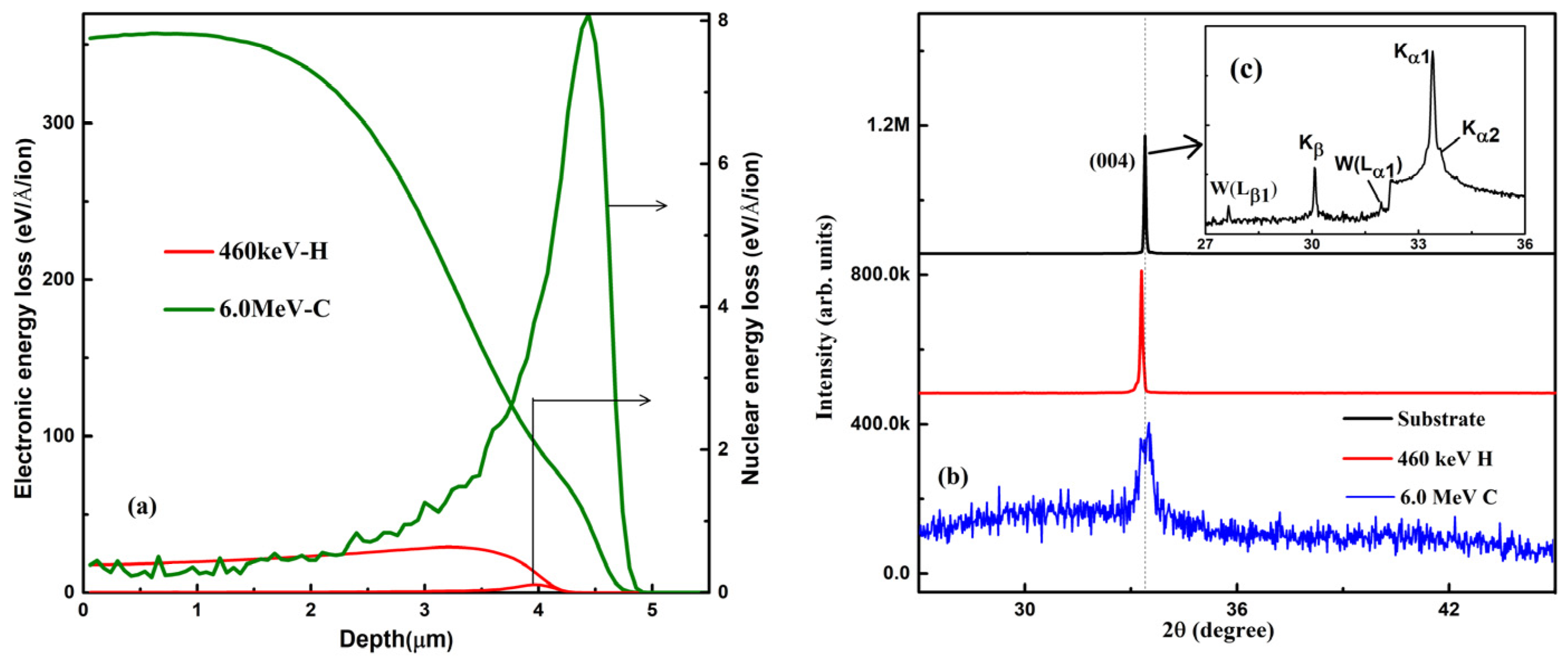
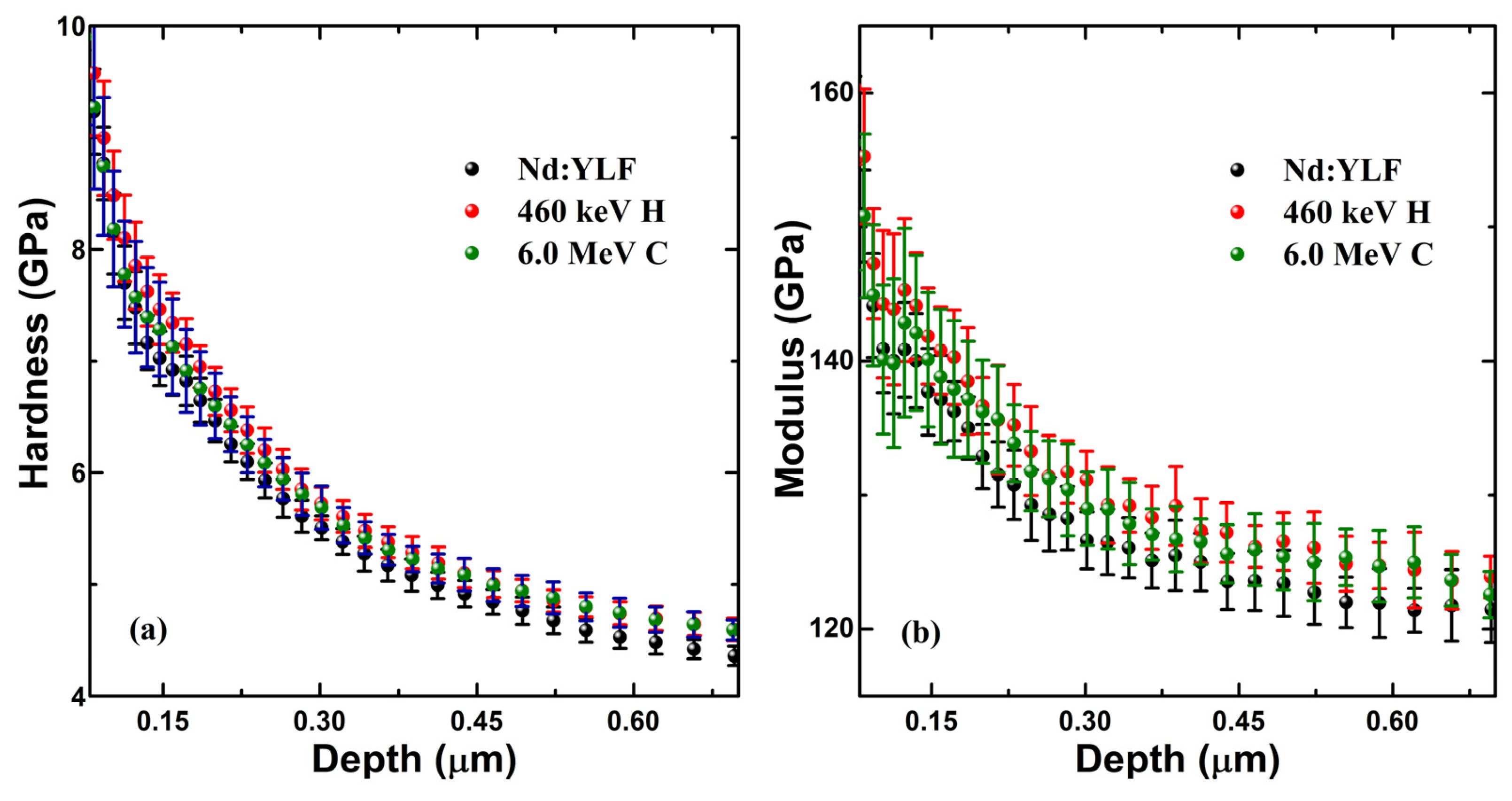
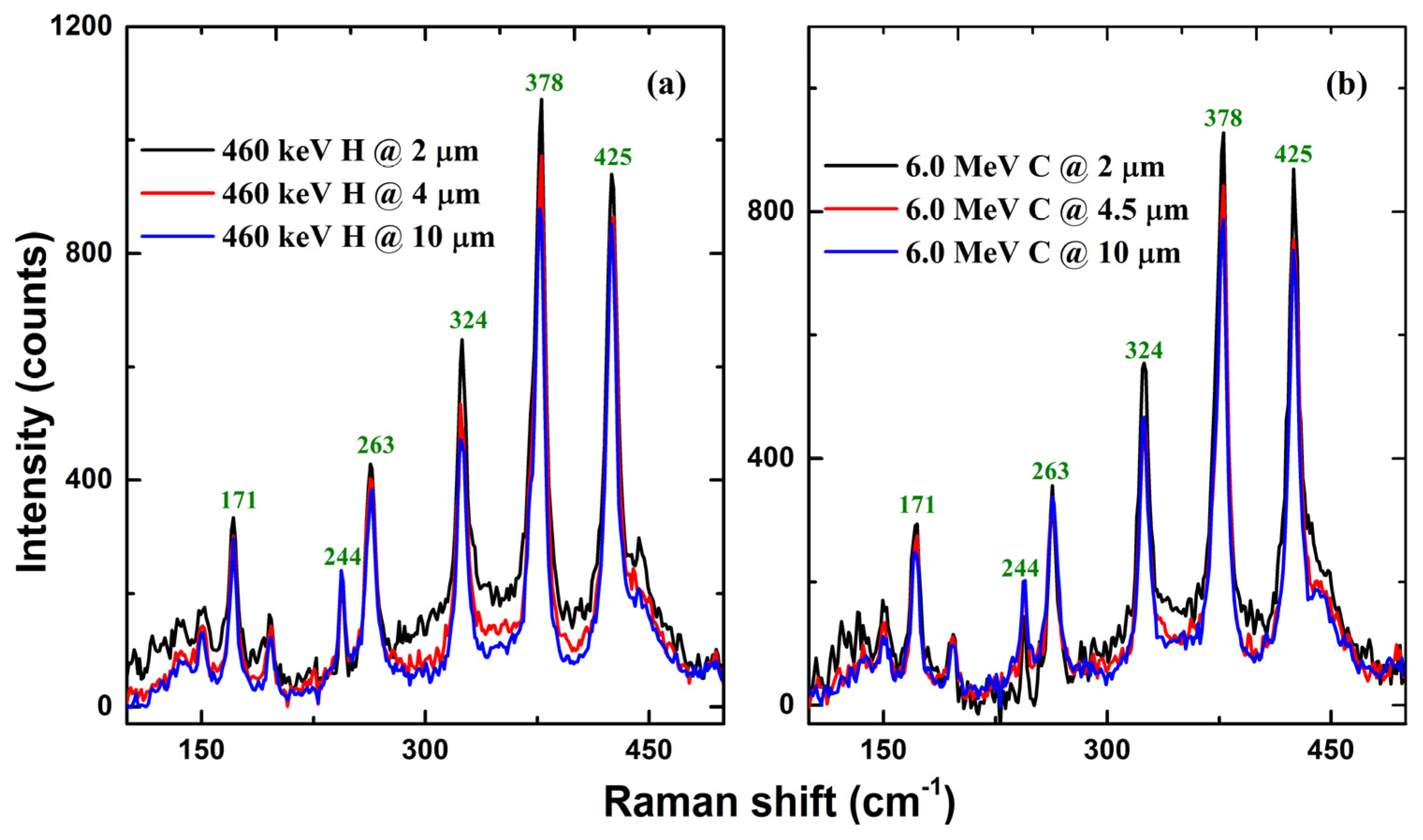
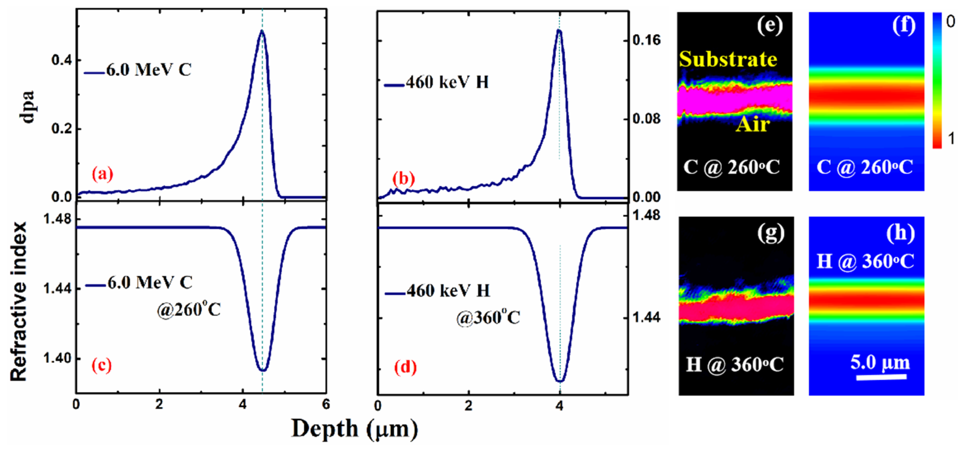
3. Results and Discussion

To analyze the energy deposition process of 460 keV H and 6.0 MeV C ions implantation in Nd:YLF, the electronic energy loss (Se) and nuclear energy loss (Sn) profiles were simulated by SRIM 2013. According to the references [23,25], although Se was two orders higher than Sn, in the case of low-energy H ion implantation and medium-energy C ion implantation, it may only induce changes in the near-surface refractive index and color centers, or removable defects, and the decrease in the refractive index in the barrier region is mainly induced by Sn. As shown in Figure 1a, Se occupies a dominant position at the sample surface. Simultaneously, the end of the ion tracks, which correspond to the stop location of the implanted ions, is governed by Sn. For 460 keV H and 6.0 MeV C ions, the Se on the surface was 17.8 eV/Å/ion and 354.1 eV/Å/ion, respectively, and the Sn at the damage peak (3.96 µm and 4.44 µm) was 0.11 eV/Å/ion and 8.09 eV/Å/ion, respectively. Obviously, whether Se or Sn, the C ion implantation at 6.0 MeV is much higher than the H ion implantation at 460 keV.
The XRD patterns of unimplanted, 460 keV H-ion-implanted and 6.0 MeV C-ion-implanted Nd:YLF samples are shown in Figure 1b. The diffraction peak in the unimplanted sample at 2θ = 33.29o corresponds to the reflections of the (004) planes. The signal around the (004) peak in unimplanted Nd:YLF is replotted to present the relatively weak peaks more clearly, and is noted in Figure 1c. As shown in Figure 1b, the diffraction peak is almost unchanged after H ion implantation, with only a slight shift to the left, indicating that little lattice damage was induced in the sample. The left shift of the diffraction peak is caused by tensile stress (lattice swelling). According to Ref. [28], the lattice swelling induced by ion implantation is initially due to the formation of cation anti-site defects. According to the Prague formula 2dsinθ = (d is the interplanar spacing, θ is the diffraction angle, n (n = 4) is the diffraction order, and λ is the X-ray wavelength), the left shift in the diffraction peak means that the interplanar spacing (or lattice parameter) increased. A relatively noisy diffraction peak with a large FWHM is shown after 6.0 MeV C ion implantation, indicating the relatively poor crystallinity of the sample surface. The above results indicate that the degree of damage to the sample surface caused by 6.0 MeV C ion implantation is significantly higher than that of 460 keV H ion implantation. The sample surface damage is mainly determined by Se, which also indicates that the results of XRD are consistent with those of the SRIM simulation calculations (shown in Figure 1a).
The mechanical properties in H- and C-ion-implanted Nd:YLF crystals were measured using the nano-indentation test. The hardness and elastic (Young’s) modulus were measured and are shown in Figure 2. The evolution of hardness generally caused by ion implantation depends on the competition between the behavior of two effects [29,30]: on the one hand, dislocation motion can be hindered by high-density defects induced by ion implantation and increased hardness, called radiation hardening; on the other hand, the crystalline lattice can be destroyed by the ion implantation process, reducing the bond’s density and hardness. As shown in Figure 2a, the hardness slightly increases after H and C ions implantation, which means that the radiation hardening effect of the implanted Nd:YLF samples was slightly stronger. In addition, the hardness of samples implanted using H ions is slightly higher than that of samples implanted via C ions, which also means that the radiation hardening of the H-implanted sample is more dominant than the change in the chemical bond’s properties. In addition, an amorphous layer was formed at the C peak concentration, resulting in a softer sample [31,32].
Figure 2b shows that the elastic modulus of samples implanted with H and C ions is higher than that of the unimplanted sample. The elastic modulus of materials can be affected by the atomic spacing and the chemical bond’s energy [33], which means that the increase in the chemical bond’s energy and decrease in the atomic spacing induced by H and C ions implantation leads to an increase in the elastic modulus.
The molecular vibration, sample density, and lattice damage induced by ion implantation [34] can be reflected by the Raman spectra. The Raman spectra were measured at different depths of the H- and C-ion-implanted Nd:YLF samples: the electronic-energy-loss-dominant region, nuclear-energy-loss-dominant region, and substrate region, respectively. Six main peaks were observed, at 171 cm−1 (Bg mode), 244 cm−1 (Bg mode), 263 cm−1 (Ag mode), 324 cm−1 (Eg and Bg modes), 378 cm−1 (Bg mode), and 425 cm−1 (Ag and Bg modes), and the modes observed above were concurrent with the previous results [35]. As shown in Figure 3, the Raman peak intensity is sequentially increased in the substrate (at 10.0 µm depth for H and C ions implantation), nuclear-energy-loss-dominant (at 4.0 and 4.5 µm for H and C ions implantation, respectively), and electronic-energy-loss-dominant region (at 2.0 µm for H and C ions implantation). Owing to the H and C ion implantation process, the atomic spacing in the ion interaction region significantly increases, leading to an increase in polarization, and thereby increasing the intensity of the Raman peak in the ion interaction region. Moreover, nuclear collisions at the end of the ion trajectory resulted in significant crystal damage, increased lattice disorder, and weakened Raman peaks. Therefore, the Raman peak intensity of the nuclear energy loss region (at 4.0 and 4.5 µm for H and C ion implantation) is lower than the electronic energy loss for H- and C-ion-implanted samples.
The absorption spectra of Nd:YLF samples were measured and are shown in Figure 4a. The absorption coefficient of Nd3+ ions can be calculated using the following equation:
α = ln ( I t / I 0 ) L
In the above equation, α is absorption coefficient; I0 and It are the intensities before and after transmission, respectively; and L (0.1 cm) is the thickness of the sample. According to the measured absorption spectra (Figure 4a), the absorption coefficients of the unimplanted and H- and C-ion-implanted samples at 804 nm are α = 2.32, 2.59, and 2.84 cm−1, respectively. Compared to the unimplanted sample, the absorption coefficient of H- and C-ion-implanted samples increased by 11.64% and 22.41%, respectively. The increased absorption coefficient is due to the change in the near-surface lattice structure, which is consistent with the results of the SRIM 2013 simulation and XRD pattern (Figure 1). As mentioned above, compared to the unimplanted crystal, the absorption peaks in the H- and C-implanted sample are apparently stronger. During the implantation process, the implanted ions will collide with lattice atoms at the implantation end range (3.96 µm and 4.44 µm for H and C ions, respectively), which leads to the displacement of lattice atoms. These defects were gradually enriched with an increase in implantation fluence, which induced lattice disorder, expansion, and even amorphization in the crystals. The color centers form in this process, enhancing the absorption of light.
As shown in Figure 4b, the micro-luminescence spectra of the unimplanted, 460 keV H-ion-implanted, and 6.0 MeV C-ion-implanted samples were measured. The emission peaks associated with the 4F3/2→4I9/2 transition at 863, 867, 876, 880, 885, 903, and 908 nm were detected [36,37,38,39]. The emission spectra obtained from the unimplanted, 460 keV H-ion-implanted, and 6.0 MeV C-ion-implanted samples were similar in their sharp and peak position. This indicates that the intrinsic fluorescence properties of the Nd3+ ions did not deteriorate due to ion implantation. The emission peak intensity decreased after ion implantation due to the implantation-induced lattice damage. The greater the lattice damage, the more the peak intensity decreases.
The dark-mode spectra of the 460 keV H-ion- and 6.0 MeV C-ion-implanted Nd:YLF samples were measured with the prism coupling technique. A schematic diagram of the prism coupling measurement is shown in Figure 5a. After H and C ions implantation, the existence of a guiding mode was not detected. To investigate the annealing effect on guiding modes, the samples were subjected to continuous annealing treatment. The specific annealing conditions are displayed in Table 1. The guiding mode was detected for the 6.0 MeV C-ion-implanted Nd:YLF sample after S1 annealing treatment at a 633 nm wavelength. It was not until after the S3 annealing treatment that the guiding mode of the 460 keV H-ion-implanted Nd:YLF sample was discovered at a 633 nm wavelength. The effective refractive index in TM0, TM1, and TM2 modes after the corresponding annealing process is shown in Figure 5b. The substrate refractive index of the Nd:YLF sample is 1.4753 in TM mode at a 633 nm wavelength. As shown in Figure 5b, the effective refractive index is lower than the substrate refractive index.
In order to describe the lattice damage in implanted samples, the dpa of Nd:YLF crystal induced by ion implantation was simulated by SRIM 2013. In Figure 6a,b, the maximum dpa is 0.49 and 0.17 at depths of 4.44 and 3.96 µm for 6.0 MeV C and 460 keV H ions implantation, respectively. The depth of the maximum dpa value is consistent with the maximum nuclear energy loss region (Figure 1a). According to the results of prism coupling at 633 nm (Figure 5b), the refractive index profiles (TM mode) of the Nd:YLF waveguides were rebuilt by the RCM and are shown in Figure 6c,d. At a depth of 4.4 µm, the refractive index was decreased to about 0.08 for 6.0 MeV C-ion-implanted Nd:YLF crystal (after S1 annealing treatment). The refractive index was decreased to about 0.06 for the 460 keV H-ion-implanted Nd:YLF crystal (after S3 annealing treatment) at a depth of 3.96 µm. It can be concluded that the refractive index will decrease with an increase in lattice damage. As shown in Figure 6, the peak positions of dpa are consistent with the position of the lowest value of the refractive index profiles, which also demonstrates the correctness of RCM simulation results.
With the restructured refractive index profile shown in Figure 6c,d, FD-BPM was used to simulate the light intensity profile of the waveguide at 633 nm in TM mode, as shown in Figure 6f,h. The corresponding near-field intensity distribution in TM mode at 633 nm was also measured via the end-face coupling method (Figure 6e,g). The results indicate that the experimental and simulated near-field intensity distributions are in agreement, which also demonstrates the correctness of the reconstructed refractive index profile presented in Figure 6c,d.
In order to investigate the lattice damage on the waveguide surface, RBS/channeling spectra were measured and are shown in Figure 7. Virgin and random spectra were measured from the untreated Nd:YLF crystal for comparison. The random spectra curve of the Nd:YLF crystal was simulated by SIMNRA, which is consistent with the measured random spectra in the experiment, indicating the reliability of the experiment. The illustration is a locally enlarged image of the RBS/channeling pattern near the surface area of the sample after converting the channel number to depth. As shown, the channeling spectra yield of the implanted samples (6.0 MeV C ion implantation after S1 annealing treatment, 460 keV H ions after S3 annealing treatment) is slightly higher than that of the unimplanted sample at a 0–200 nm depth. The results indicate that there is no significant lattice damage on the surface of the penetration region (Se-dominant region) after appropriate annealing treatment. As shown in Figure 6a,b, at a depth of 200 nm, the value of the dpa is very low, which is consistent with the RBS/channeling spectra results.
The electrical properties of the Nd:YLF samples were measured by semiconductor parameter analyzers and probe stations at room temperature. The I-V characteristic curve of the Nd:YLF crystal and the H- (after S3 annealing treatment) and C- (after S1 annealing treatment) ion-implanted Nd:YLF crystal are shown in Figure 8. The I-V characteristic curve of the Nd:YLF sample is basically a linear curve. The resistivity (ρ) can be simulated with the following formula:
ρ = R S / L
R, S, and L represent the resistance, cross-sectional area, and length of the samples, respectively. The resistivity ρ of the Nd:YLF crystal and Nd:YLF crystal with H (after S3 annealing treatment) and C (after S1 annealing treatment) ion implantation were calculated to be 4.57 × 10⁶ Ω·m, 2.60 × 10⁸ Ω·m, and 6.00 × 10⁸ Ω·m, respectively. Compared to H ion implantation, the lattice damage caused by C ion implantation is relatively greater. Therefore, the resistivity after C ion implantation is higher than that of H ion implantation. According to the above results, the conductivity of the Nd:YLF crystals can be effectively regulated by selecting appropriate implantation conditions, and the characteristics of waveguide sensors can be measured by changing their electrical properties.
In this work, in order to study the irradiation effects of Nd:YLF crystals using different kinds of ions (light ions and medium-mass ions) with a similar implantation depth, the Nd:YLF samples were implanted using H (with an energy of 460 keV and a fluence of 5.6 × 10¹⁶ ions/cm2) and C (with an energy of 6.0 MeV and a fluence of 3.0 × 10¹⁵ ions/cm2) ions. First of all, the lattice damage as well as the spectral and structural properties of the Nd:YLF crystals implanted with H and C ions are discussed in detail with XRD patterns, Raman spectroscopy, absorption spectroscopy, fluorescence spectroscopy, and nano-indentation results, which indicates that the degree of lattice damage caused by C ion implantation was significantly higher than that which occurred with H ion implantation. The SRIM code was used to simulate the lattice damage induced by H and C ions implantation, showing that the maximum dpa of C ion implantation is about three times higher than that of H ion implantation. Moreover, the Nd:YLF crystals implanted with C ions are likely to have amorphous layers in the region where nuclear energy loss is dominant. Secondly, the Nd:YLF waveguides were formed after annealing treatment, the properties were studied through prism coupling and the end-face coupling method, and the “barrier” type waveguides could afford a guiding mode at wavelength of 633 nm. Finally, the electrical properties and near-surface lattice damage in the Nd:YLF crystals after annealing were studied via I-V characteristic curves and RBS/channeling technology, respectively.

4. Conclusions

In summary, the structural properties, damage behavior, spectral characteristics, waveguides, and electrical properties of H- and C-ion-implanted Nd:YLF crystals were discussed using complementary characterization techniques. The changes in the FWHM of the XRD pattern, the hardness and elastic modulus, the Raman spectra, the absorption spectra, and the fluorescence spectra show the lattice structure disorder that occurs after H and C ions implantation. The “barrier”-type optical waveguide structure was formed after annealing through 460 keV H and 6.0 MeV C ions implantation. The physical properties of the waveguide (the effective refractive index, refractive index profile, thickness of the optical barrier, degree of damage on the waveguide surface, etc.) caused by the lattice structure disorder following H and C ion implantation were discussed in detail. The formation of waveguide structures shows unique potential in the application of highly sensitive optoelectronic sensors.

Author Contributions

M.Q.: methodology, formal analysis, writing—original draft preparation, and writing—review and editing; T.W.: methodology and formal analysis; Y.L.: software and data curation; W.C.: data curation and validation; X.W.: investigation; Z.W.: data curation and validation; X.L.: software and data curation; S.X.: methodology and formal analysis. All authors have read and agreed to the published version of the manuscript.

Funding

This work was supported by the National Natural Science Foundation of China (Grant Nos. 12105036 and 12274058), the Natural Science Foundation of Shandong Province of China (Grant Nos. ZR2020QA088 and ZR2021QA074), the Taishan Scholars Program of Shandong Province (Grant No. tsqn201812104), and the Qingchuang Science and Technology Plan of Shandong Province (Grant No. 2019KJJ017).

Data Availability Statement

Data are contained within this article.

Conflicts of Interest

The authors declare no conflicts of interest.

References

  1. Vieira, T.D.A.; Prado, F.M.; Wetter, N.U. Nd:YLF laser at 1053 nm diode side pumped at 863 nm with a near quantum-defect slope efficiency. Opt. Laser Technol. 2022, 149, 107818. [Google Scholar]
  2. Turri, G.; Webster, S.; Bass, M.; Toncelli, A. Temperature-Dependent Stimulated Emission Cross-Section in Nd3+:YLF Crystal. Materials 2021, 14, 431. [Google Scholar] [CrossRef]
  3. Fornasiero, L.; Kellner, T.; Kück, S.; Meyn, J.P.; Möbert, P.E.-A.; Huber, G. Excited state absorption and stimulated emission of Nd3+ in crystals III: LaSe3(BO3)4, CaWO4, and YLiF4. Appl. Phys. B 1999, 68, 62–72. [Google Scholar] [CrossRef]
  4. Xu, S.; Gao, S. A new wavelength laser at 1370 nm generated by Nd:YLF crystal. Mater. Lett. 2016, 183, 451–453. [Google Scholar] [CrossRef]
  5. Tu, Z.H.; Dai, S.B.; Zhu, S.Q.; Yin, H.; Li, Z.; Ji, E.C.; Chen, Z.Q. Efficient high-power orthogonally-polarized dual-wavelength Nd:YLF laser at 1314 and 1321 nm. Opt. Express 2019, 27, 32949–32957. [Google Scholar] [CrossRef]
  6. Sousa, E.C.; Camargo, F.A.; Raniere, I.M.; Baldochi, S.L.; Wetter, N.U. CW Operation of Diode Side Pumped Nd:YLF Laser. 2007. Available online: https://www.oasisbr.ibict.br/vufind/Record/IPEN_097d53b15b854cb516c687ee01d3bae1 (accessed on 7 December 2023).
  7. Turri, G.; Gennari, F.; Bass, M.; Toncelli, A. Mid-infrared spectroscopy of Nd:YLF crystal. J. Lumin. 2022, 246, 118842. [Google Scholar] [CrossRef]
  8. Zuo, Z.Y.; Dai, S.B.; Zhu, S.Q.; Yin, H.; Li, Z.; Chen, Z.Q. Power scaling of an actively Q-switched orthogonally polarized dual-wavelength Nd:YLF laser at 1047 and 1053 nm. Opt. Lett. 2018, 43, 4578–4581. [Google Scholar] [CrossRef] [PubMed]
  9. Liang, H.C.; Wu, C.S. Diode-pumped orthogonally polarized selfmode-locked Nd:YLF lasers subject to gain competition and thermal lensing effect. Opt. Express 2017, 25, 13697–13704. [Google Scholar] [CrossRef] [PubMed]
  10. Sedaghati, Z.; Nadimi, M.; Major, A. Efficient continuous-wave Nd:YLF laser in-band diode-pumped at 908nm and its thermal lensing. Laser Phys. Lett. 2019, 16, 125002. [Google Scholar] [CrossRef]
  11. Tang, Y.; Luo, Q.; Chen, Y.; Xu, K. All-silicon photoelectric biosensor on chip based on silicon nitride waveguide with low loss. Nanomaterials 2023, 13, 914. [Google Scholar] [CrossRef]
  12. Xu, X.; Yin, Y.; Sun, C.; Li, L.; Lin, H.; Tang, B.; Zhang, P.; Chen, C.; Zhang, D. Optical Temperature Sensor Based on Polysilicon Waveguides. Sensors 2022, 22, 9357. [Google Scholar] [CrossRef]
  13. Zhou, J.; Shao, Q.; Tang, C.; Qiao, F.; Lu, T.; Li, X.; Liu, X.; Zhao, H. Conformable and compact multiaxis tactile sensor for human and robotic grasping via anisotropic waveguides. Adv. Mater. Technol. 2022, 7, 2200595. [Google Scholar] [CrossRef]
  14. Rose, T.S.; Hopkins, M.S.; Fields, R.A. Characterization and control of gamma and proton radiation effects on the performance of Nd:YAG and Nd:YLF Lasers. IEEE J. Quantum Electron. 1995, 31, 9. [Google Scholar] [CrossRef]
  15. Dhoble, S.J.; Deshpande, S.P.; Pode, R.B.; Dhoble, N.S.; Gundurao, T.K. Radiation-induced defects in Pr3+-activated LiYF4 laser host. Radiat. Eff. Defect. Solids 2004, 159, 667–679. [Google Scholar] [CrossRef]
  16. Peakheart, D.W. Radiation-induced defects in lithium yttrium fluoride. Radiat. Eff. Defect. Soilds 1997, 143, 213–224. [Google Scholar] [CrossRef]
  17. Morato, S.P.; Macedo, T.C.A. F and photochromic centers in LiYF4: Nd crystals. Radiat. Eff. 1983, 72, 229–235. [Google Scholar] [CrossRef]
  18. Song, X.X.; Wang, Y.; Li, S.; Jia, C.L. The formation and characterization of optical waveguide in Nd:YLF crystal by 4.5-MeV Si ion implantation. Phys. B Condens. Matter 2019, 552, 209–213. [Google Scholar] [CrossRef]
  19. Lee, T.; Kim, J.; An, S.; Jeong, S.; Lee, D.; Jeong, D.; Lee, N.J.; Lee, K.; You, C.; Park, B.; et al. Field-free spin-orbit torque switching of GdCo ferrimagnet with broken lateral symmetry by He ion irradiation. Acta Mater. 2023, 246, 118705. [Google Scholar] [CrossRef]
  20. Wang, J.P.; Guo, L.; Luo, J.R.; Song, J.F.; Shi, Y.; Chen, C.A. In-situ TEM investigation of dislocation loop evolution in HR3 steel during Fe+ ion irradiation. J. Nucl. Mater. 2023, 578, 154309. [Google Scholar] [CrossRef]
  21. He, Z.; Theodosiou, A.; Cai, M.; Smith, A.; Jones, A.; Marsden, B.; Huang, H.; Zhou, X. Estimating the dimensional change behavior of nuclear graphite with heavy-ion irradiation-induced bending. Carbon 2023, 204, 357–366. [Google Scholar] [CrossRef]
  22. Daghbouj, N.; AlMotasem, A.T.; Vesely, J.; Li, B.S.; Sen, H.S.; Karlik, M.; Lorincík, J.; Ge, F.F.; Zhang, L.; Krsjak, V.; et al. Microstructure evolution of iron precipitates in (Fe, He)-irradiated 6H-SiC: A combined TEM and multiscale modeling. J. Nucl. Mater. 2023, 584, 154543. [Google Scholar] [CrossRef]
  23. Tan, Y.; Chen, F.; Wang, L.; Jiao, Y. Carbon ion-implanted optical waveguides in Nd:YLiF4 crystal: Refractive index profiles and thermal stability. Nucl. Instrum. Mater. B 2007, 260, 567–570. [Google Scholar] [CrossRef]
  24. Tan, Y.; Chen, F. Experimental observation and numerical simulation of guided modes in Nd: YLiF4 channel waveguides produced by carbon ion implantation. Phys. Status Solidi-R 2007, 1, 277–279. [Google Scholar] [CrossRef]
  25. Tan, Y.; Chen, F.; Wang, L.; Lu, Q.M. Optical planar waveguides in Nd: YLiF4 crystal fabricated by proton implantation. Phys. Status Solidi A 2007, 204, 3170–3173. [Google Scholar] [CrossRef]
  26. Ziegler, J.F.; Ziegler, M.D.; Biersack, J.P. SRIM-the stopping and range of ions in matter (2010). Nucl. Instrum. Mater. B 2010, 268, 1818–1823. [Google Scholar] [CrossRef]
  27. Ziegler, J.F. Interactions of Ions with Matter. Available online: www.srim.org (accessed on 7 December 2023).
  28. Li, Y.H.; Uberuaga, B.P.; Jiang, C.; Choudhury, S.; Valdez, J.A.; Patel, M.K.; Won, J.; Wang, Y.-Q.; Tang, M.; Safarik, D.J.; et al. Role of antisite disorder on preamorphization swelling in titanate pyrochlores. Phys. Rev. Lett. 2012, 108, 195504. [Google Scholar] [CrossRef] [PubMed]
  29. Xu, C.L.; Zhang, C.H.; Li, J.J.; Zhang, L.Q.; Yang, Y.T.; Song, Y.; Li, X.J.; Chen, K.Q. A HRXRD and nano-indentation study on Ne-implanted 6H-SiC. Nucl. Instrum. Mater. B 2012, 286, 129–133. [Google Scholar] [CrossRef]
  30. Costantini, J.M.; Kerbiriou, X.; Sauzay, M.; Thome, L. Ion-beam modifcations of mechanical and dimensional properties of silicon carbide. J. Phys. D Appl. Phys. 2012, 45, 465301. [Google Scholar] [CrossRef]
  31. Sommer, M.; Ebner, G.; Decho, H.; Hoja, S.; Fechte-Heinen, R. Surface preparation for characterization of nitride compound layers using hardness indentation and the Palmqvist method. J. Mater. Res. Technol. 2023, 24, 7974–7988. [Google Scholar] [CrossRef]
  32. Li, Z.M.; Zhang, L.M.; Jiang, W.L.; Pan, C.L.; Meng, X.; Chen, L. Hardness variation in nanocrystalline SiC irradiated with heavy ions. Ceram. Int. 2022, 48, 17846–17851. [Google Scholar] [CrossRef]
  33. Hu, S.W.; Li, T.J.; Su, Z.Q.; Liu, D.X. Research on suitable strength, elastic modulus and abrasion resistance of Ti–Zr–Nb medium entropy alloys (MEAs) for implant adaptation. Intermetallics 2022, 140, 107401. [Google Scholar] [CrossRef]
  34. Leide, A.J.; Lloyd, M.J.; Todd, R.I.; Armstrong, D.E.J. Raman spectroscopy of ion irradiated SiC: Chemical defects, strain, annealing, and oxidation. arXiv 2020, arXiv:2004.14335. [Google Scholar]
  35. Zhang, X.X.; Schulte, A.; Chai, B.H.T. Raman, spectroscopic evidence for isomorphous structure of GdLiF4 and YLiF4 laser crystals. Solid State Commun. 1994, 89, 181–184. [Google Scholar] [CrossRef]
  36. Hur, M.G.; Yang, W.S.; Suh, S.J.; Ivanov, M.A.; Kochurikhin, V.V.; Yoon, D.H. Optical properties of EFG grown Nd:YVO4 single crystals dependent on Nd concentration. J. Cryst. Growth 2002, 237–239, 745–748. [Google Scholar] [CrossRef]
  37. Cali, C.; Cornacchia, F.; Di Lieto, A.; Marchetti, F.; Tonelli, M. Nd: YVO4 crystalline film grown by pulsed laser deposition. Opt. Mater. 2009, 31, 1331–1333. [Google Scholar] [CrossRef]
  38. Zhang, H.J.; Meng, X.L.; Zhu, L.; Wang, C.Q.; Chow, Y.T.; Lu, M.K. Growth, spectra and influence of annealing effect on laser properties of Nd:YVO4 crystal. Opt. Mater. 2000, 14, 25–30. [Google Scholar] [CrossRef]
  39. Buissette, V.; Huignard, A.; Gacoin, T.; Boilot, J.P.; Aschehoug, P.; Viana, B. Luminescence properties of YVO4: Ln (Ln=Nd, Yb, and Yb-Er) nanoparticles. Surf. Sci. 2003, 532–535, 444–449. [Google Scholar] [CrossRef]
Figure 1. (a) The Se and Sn as a function of the penetration depth for 460 keV H and 6.0 MeV C ions implanted into Nd:YLF sample based on SRIM 2013 simulation; (b) the XRD pattern (θ–2θ) of unimplanted sample, 460 keV H-ion-implanted and 6.0 MeV C-ion-implanted samples; (c) local amplification patterns around (004) peak in virgin Nd:YLF.
Crystals 14 00146 g001
Figure 2. (a) The hardness and (b) modulus of unimplanted and H- and C-ion-implanted Nd:YLF samples as a function of indentation depth.
Crystals 14 00146 g002
Figure 3. The Raman spectra of (a) H- and (b) C-ion-implanted Nd:YLF samples at different detection positions: electronic-energy-loss-dominant region (red line), nuclear-energy-loss-dominant region (blue line), substrate region (black line).
Crystals 14 00146 g003
Figure 4. (a) Absorption spectra and (b) nonpolarized fluorescence spectra of unimplanted (black dashed line), 460 keV H-ion-implanted (red dashed line), and 6.0 MeV C-ion-implanted (blue dashed line) Nd:YLF samples.
Crystals 14 00146 g004
Figure 5. (a) The schematic diagram of prism coupling measurement; (b) the effective refractive index (at 633 nm wavelength) in TM0, TM1 and TM2 modes of implanted Nd:YLF crystals after corresponding annealing treatment.
Crystals 14 00146 g005
Figure 6. (a,b): the dpa profiles for the Nd:YLF crystal implanted by 6.0 MeV C and 460 keV H ions, respectively; (c,d): reconstructed refractive index profile (TM mode) after appropriate annealing treatment. The near-field intensity distribution in TM mode at 633 nm: (e,g) intensity profile measured via the end-face coupling method; (f,h) simulated intensity profile by FD-BPM.
Crystals 14 00146 g006
Figure 7. RBS/channeling spectra of the 6.0 MeV C ion implanted after S1 annealing treatment, 460 keV H ions implanted after S3 annealing treatment of Nd:YLF samples, and the virgin and random spectra of Nd:YLF crystal. The inset is a partially enlarged view of the yield and the ion penetration depth measured in the experiment.
Crystals 14 00146 g007
Figure 8. I-V curve at room temperature: unimplanted Nd:YLF crystal corresponds to the left ordinate; Nd:YLF crystal with H (after S3 annealing treatment) and C (after S1 annealing treatment) ion implantation correspond to the right ordinate.
Crystals 14 00146 g008
Table 1. The specific annealing process of ions implanted Nd:YLF samples in the air.
ProcessAnnealing Condition
S0As implanted
S1S0 + 260 °C for 60 min
S2S1 + 310 °C for 60 min
S3S2 + 360 °C for 30 min
Disclaimer/Publisher’s Note: The statements, opinions and data contained in all publications are solely those of the individual author(s) and contributor(s) and not of MDPI and/or the editor(s). MDPI and/or the editor(s) disclaim responsibility for any injury to people or property resulting from any ideas, methods, instructions or products referred to in the content.

