1. Introduction
There are two main factors determining the electric charge transport inside active layers of organic electronic devices: the molecular structure of the molecules constituting the layer and the supra-molecular organization of the layer. The first one depends on the current abilities of organic synthesis, which, until present, has achieved very high precision in adjusting the electronic properties of the molecules through their chemical modification [
1,
2,
3,
4]. The second one depends on interactions between the molecules and direct interactions between the substrate and the molecules. The charge transport in an organic semiconducting layer is directional. It prefers a characteristic direction. In the case of low-molecular-weight semiconductors, this is the direction of π stacking. Molecular disorder along this direction substantially lowers charge carrier mobility. It is therefore important from a practical point of view to produce optimally arranged organic films to minimize the negative effects of molecular disordering on the film’s conductivity. There is also still very little known about the substrate’s influence on the interactions responsible for the π stacking.
The N,N′-dioctyl-3,4:9,10-perylene tetracarboxylic diimide (PTCDI-C8) is one of the best n-type organic semiconductors currently available [
5,
6,
7,
8]. The electron mobility measured for organic thin-film transistors based on PTCDI-C8 equals up to ~1.7 cm
2/Vs [
5]. The molecule (C
40H
42O
4N
2) consists of a planar core and two alkyl chains on opposite sides. Its high molecular stability in air enables its operation in ambient conditions. The PCTDI-C8 molecules relatively easily organize themselves into supra-molecular architectures through hydrogen bonding, metal ion coordination and π stacking [
9,
10]. There are few studies on the properties of PTCDI-C8 thin films and they have been performed on various substrates such as SiO
2 and Al
2O
3; so far these molecules have not been studied on GaN(0001) [
11,
12].
GaN(0001) is the most frequently studied surface of gallium nitride (GaN). In combination with thin organic films, GaN surfaces offer several unique properties. The wide band gap of GaN allows optical access through the substrate and makes it easier to align the highest occupied and lowest unoccupied molecular orbitals of the organic film with the substrate band edges. It permits more flexibility in device design and, in the case of applications dependent on the charge transport across the interface, it increases the possibility for molecular control of the electronic properties of the hybrid organic–inorganic system [
13,
14,
15]. Due to its high electron mobility, chemical stability under physiological conditions, non-toxicity and biocompatibility, GaN is a very attractive material for biosensors [
16,
17,
18,
19]. It has been shown that by using the GaN thin-film high-electron-mobility transistors one can electrically detect proteins, antibodies, glucose and strands of DNA selectively and with high sensitivity [
17,
18].
The aim of the study reported herein is to characterize substrates’ influence on the morphological, structural and electronic properties of PTCDI-C8 adsorption films on GaN(0001). The decisive factor for undertaking these experiments has been a willingness to identify substrate properties that have an influence on both the type of direct chemical bond between the molecules and the substrate and on the nature of the intermolecular bonds between the molecules inside the adsorption layer as well.
2. Experimental Details
The substrates used were 10 µm thick, (0001)-oriented, p-GaN (Mg-doped, 1018 cm−3) and n-GaN (Si-doped, 1018 cm−3) epitaxial layers deposited on Al2O3 (Technologies and Devices International, An Oxford Instruments Company, Oxford, UK). Typical size of the sample was about 4 × 8 mm2. The samples were ex situ degreased in isopropanol, and then washed in distilled water and dried in air. Before organic film evaporation, the substrate was in situ annealed at about 800 °C to remove any residual gases. This procedure allowed for the reduction of oxygen and carbon contaminations; however, they were not completely eliminated.
The samples were characterized in two separate UHV setups at room temperature (RT), using scanning tunneling microscopy (STM), X-ray photoelectron spectroscopy (XPS), ultraviolet photoelectron spectroscopy (UPS) and low-energy electron diffraction (LEED) techniques. The first setup included a VT STM/AFM microscope (Omicron,). The imaging was accomplished in the constant current mode using a tungsten tip. WSxM software(version number 5.0) was applied to analyze the STM results [
20]. The XPS/UPS measurements were performed in the second UHV setup, equipped with Mg and Al anodes (Mg Kα (1253.6 eV) and Al Kα (1486.6 eV) lines) and a He I line (21.2 eV) radiation source. Due to the signals overlapping the Mg anode was used for the substrates N 1s and Ga 3d’s lines measurements; the adsorbates C 1s and O 1s’ lines were measured using the Al anode. Emitted photoelectrons were collected by a hemispherical electron energy analyzer (Phoibos 100-5, SPECS, Germany) with a pass energy of 10 or 2 eV and step size of 0.1 or 0.025 eV for core-level lines or a valance band, respectively. Optical axis of the analyzer entrance was normal to the substrate surface. The Fermi level position (
EF) was found by UPS measurement on a clean Au sample. The threshold of photoemission, which corresponds to the vacuum level of the sample, was also measured with a voltage (−5 V) applied to the samples to clear the detector’s work function. The XPS spectra were analyzed using KolXPD (
Kolibrik.net, Prague, Czech Republic) and/or CasaXPS software (version number 2.3.19 PR1.0). Deconvolution of the XPS peaks was modeled using Gaussian and Lorentzian line shapes and a Shirley-type background subtracting. LEED measurements were carried out in the energy range 0–300 eV with a step of 0.5 eV; diffraction patterns were recorded using a CCD camera.
Organic films of PTCDI–C8 molecules (98% purity, Sigma-Aldrich, MilliporeSigma, Burlington, MA, USA) were deposited by physical vapor deposition (PVD) on the substrates kept at room temperature (RT) under UHV, with a base pressure of ~10
–10 Torr. The temperature of the quartz crucible used as the evaporator was about 300 °C. The evaporation rate at this temperature did not exceed 0.6 nm/min. The efficiency of the evaporator was calibrated by means of a quartz crystal resonator. The organic film growth and its characterization were performed step by step. In the case of XPS/UPS measurements, the average thickness of PTCDI-C8 films was additionally controlled on the bases of the Ga 3d substrate’s line intensity decay (measured with the Mg anode) following the progress of adsorption layer growth, assuming a mean free path of electrons λ in PTCDI-C8 layer equal to 2.84 nm [
21]. In the case of STM observations, the amount of deposited adsorbate was counted directly from the STM topographies.
4. Discussion
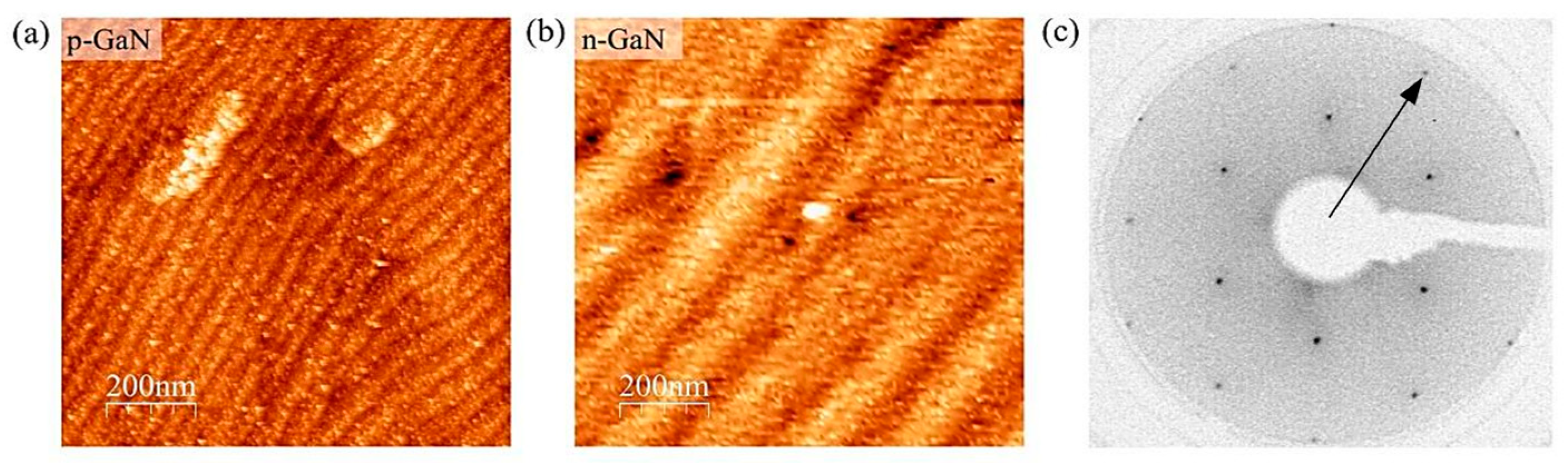
The STM topographies clearly show that carbon and oxygen residues, detected by XPS after applying the same cleaning procedures, were not uniformly distributed over the substrate surface. Instead, they were concentrated in groups, leaving an extended area of the substrate clean, with a characteristic terrace topography.
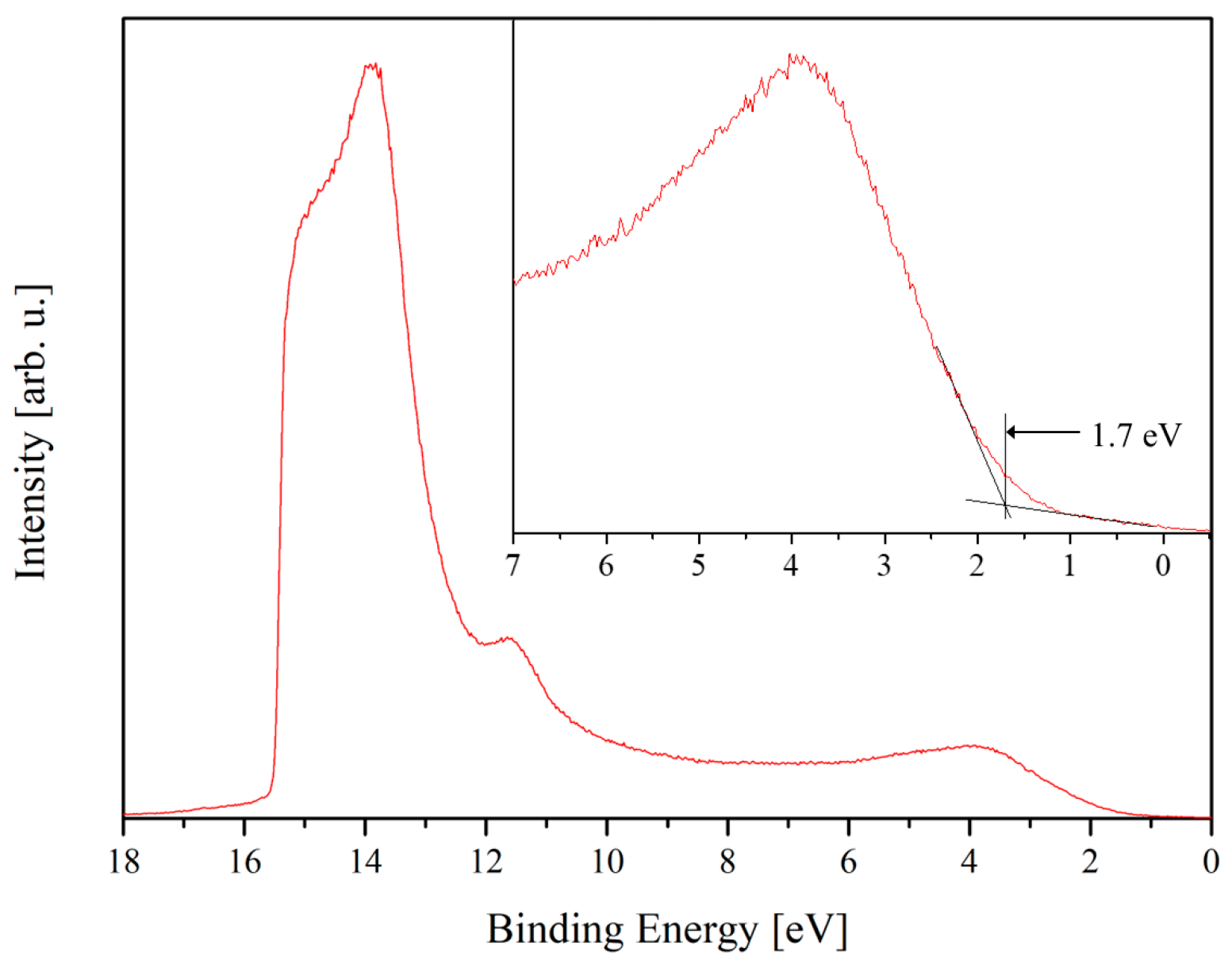
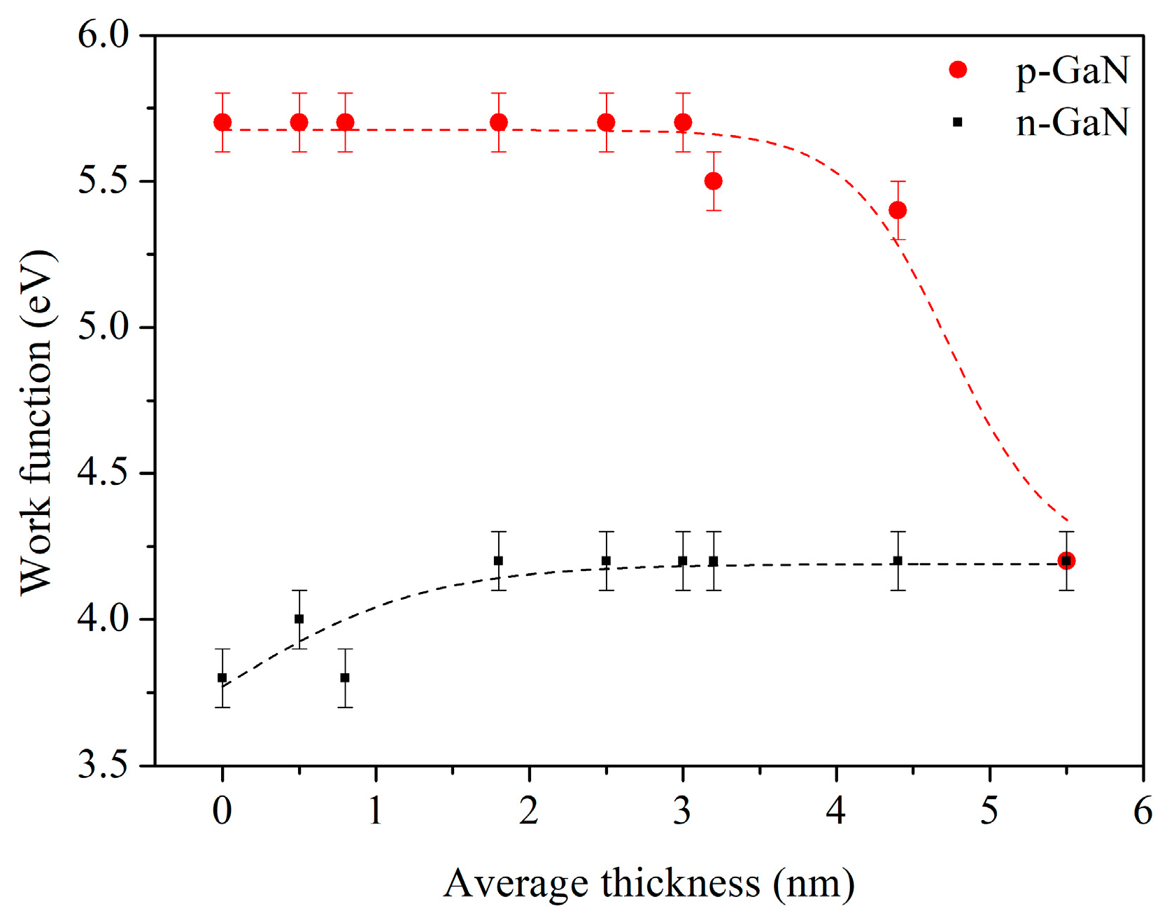
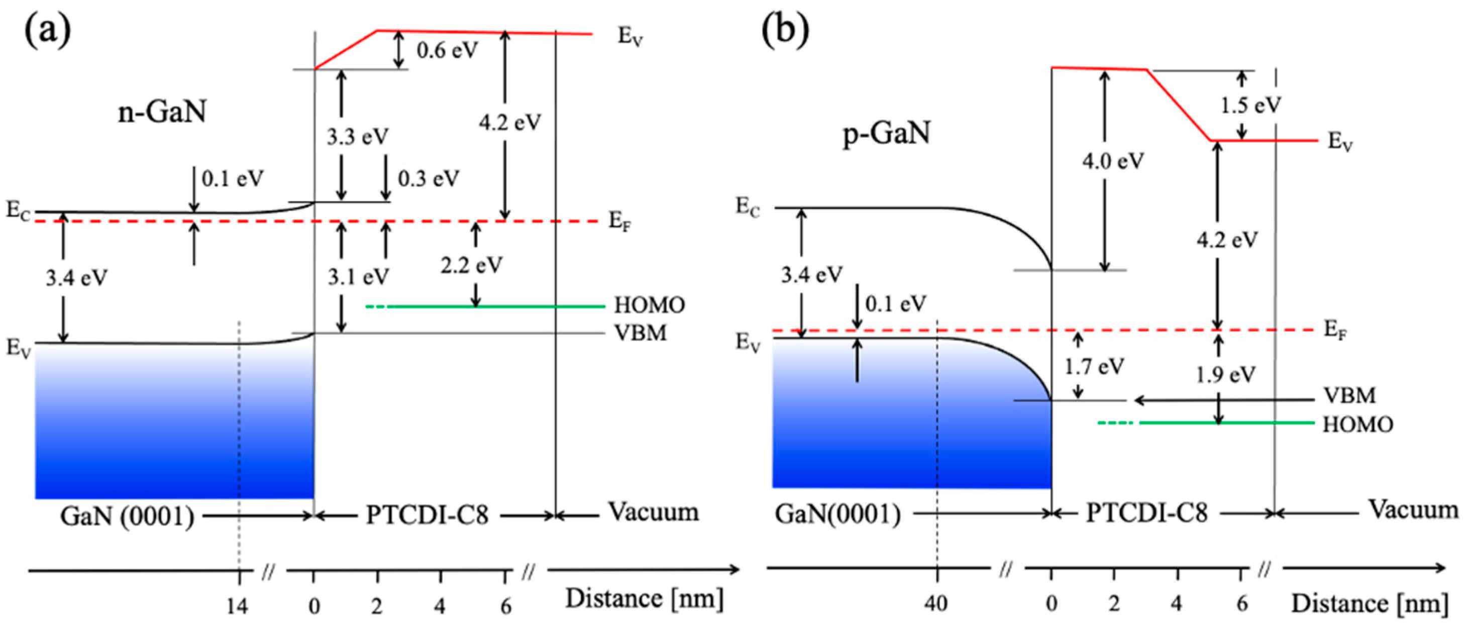
It is obvious that n- and p-type samples essentially differ in their electron structure. p-GaN(0001) has a work function
ϕ = 5.7 eV and electron affinity
χ = 4.0 eV. The n-type sample has lower values for its work function and electron affinity, respectively, 3.6 eV and 3.3 eV. The important features of the electron band structure of the PTCDI-C8/GaN(0001) interfaces are collected in the diagrams in
Figure 11a,b. The
EF, in bulk, is located 3.3 eV and 0.1 eV above the valence band maximum (
EV) for the n- and the p-type samples, respectively [
23]. The surface band bending at the vacuum/GaN(0001) interface for bare substrates, as calculated from the equation
, is equal to 0.2 eV for the n-type and 1.6 eV for the p-type sample. The bending comes from electrostatic surface charging. Solving Poisson’s equation, the space-charge region width
can be obtained, where
[
25] is the dielectric constant of GaN,
represents the permittivity of free space and q is the elementary charge of an electron. The depletion layer width amounts to about 14 nm for n-GaN and about 40 nm in the case of p-GaN. Corrections connected to surface photovoltage (SPV) effects are not considered in the above estimations. It is known that, in the case of GaN, the SPV due to UPS or XPS radiation is determined to be ~0.5 V in magnitude [
24]. In contrary to n-GaN, the band bending of p-GaN is strong due to the considerable depletion of holes in the near-surface region, caused by surface states which originate from Ga dangling bonds [
26,
27], thus, the Fermi level is pinned to these states, situating itself in the middle of the energy band gap [
28,
29,
30].
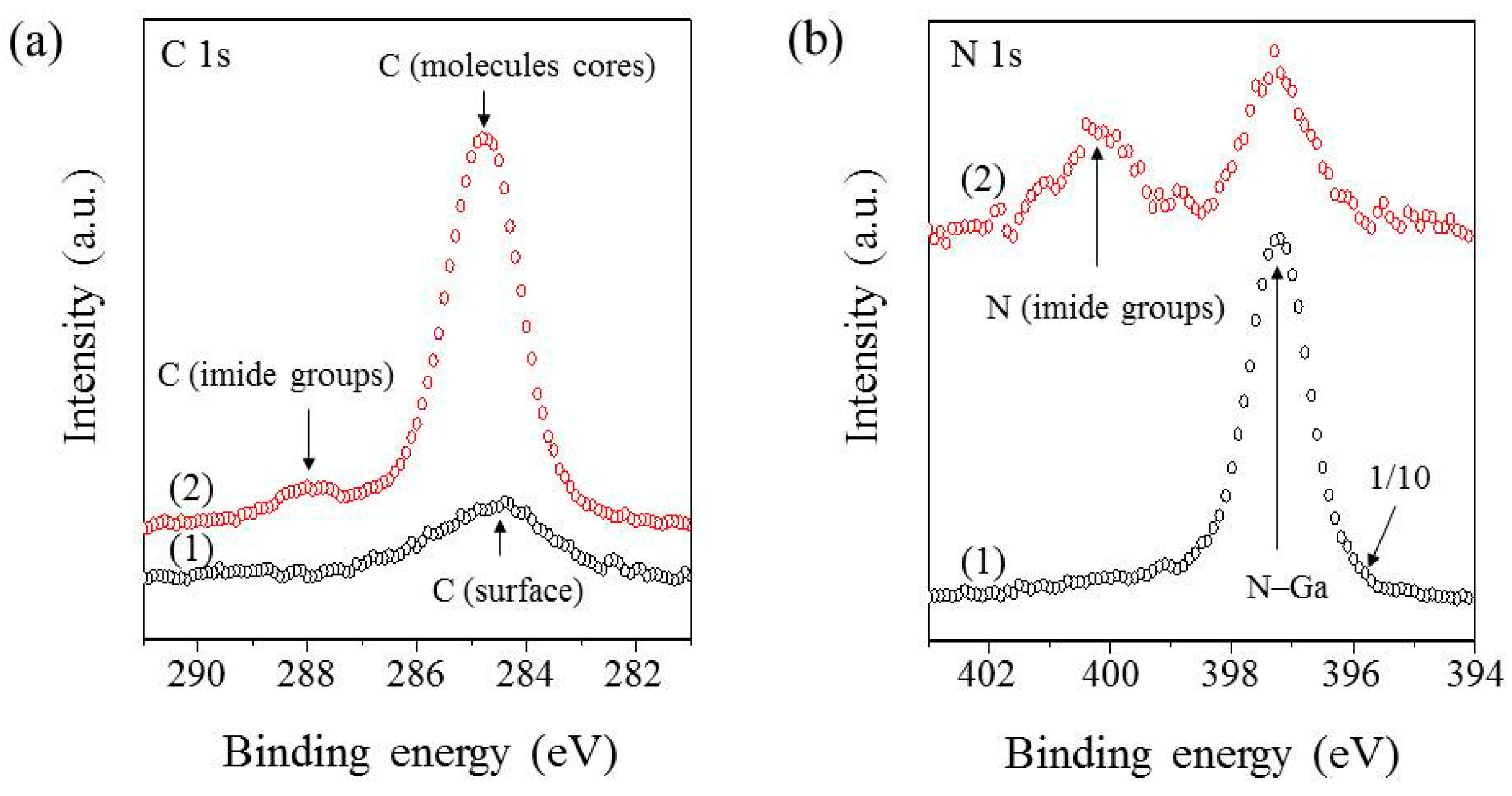
From the XPS measurements it is seen that the interaction between the substrate and PTCDI-C8 film is very weak, and rather of a Van der Walls character. A stronger chemical interaction can be excluded because the Ga 3d and N 1s lines of the substrate do not change their positions or shapes following the first and successive doses of PTCDI-C8 deposition. Also, the C 1s lines originating from the imide group or from the core of the PTCDI-C8 molecule (
Figure 6a), as well as the N 1s line from the imide group (
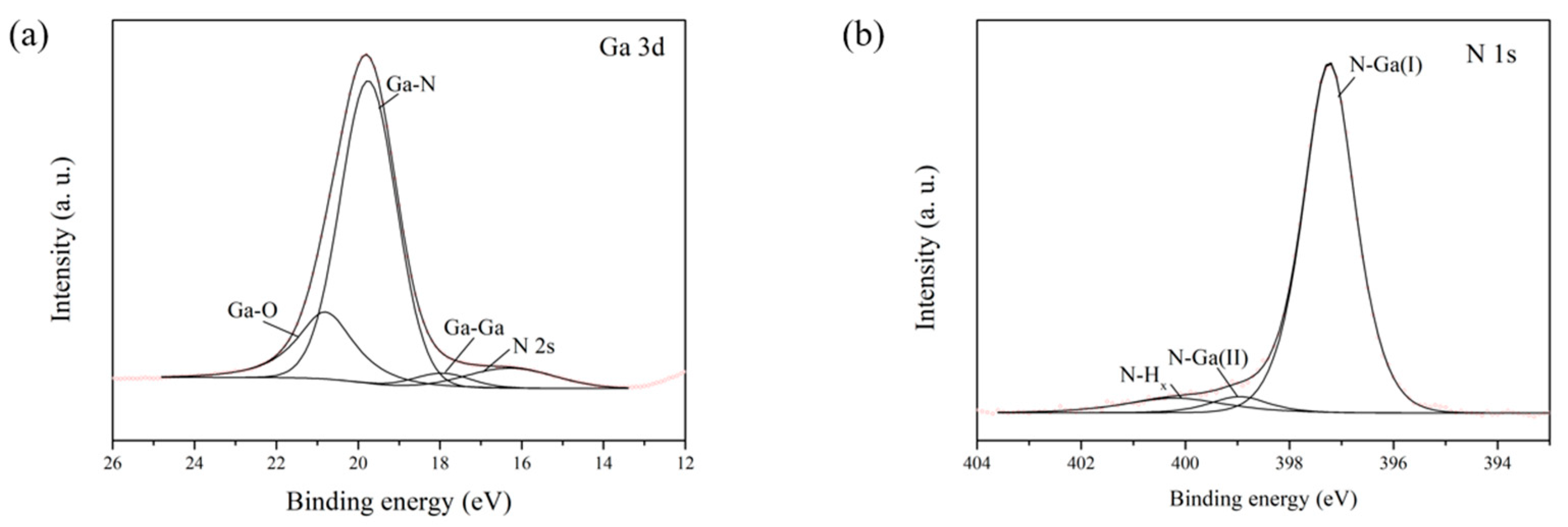
Figure 6b), do not change their positions or shapes following the film growth. Taking these into account, it can be safely assumed that the influence of the PTCDI-C8 film on the band bending of the substrate can be neglected.
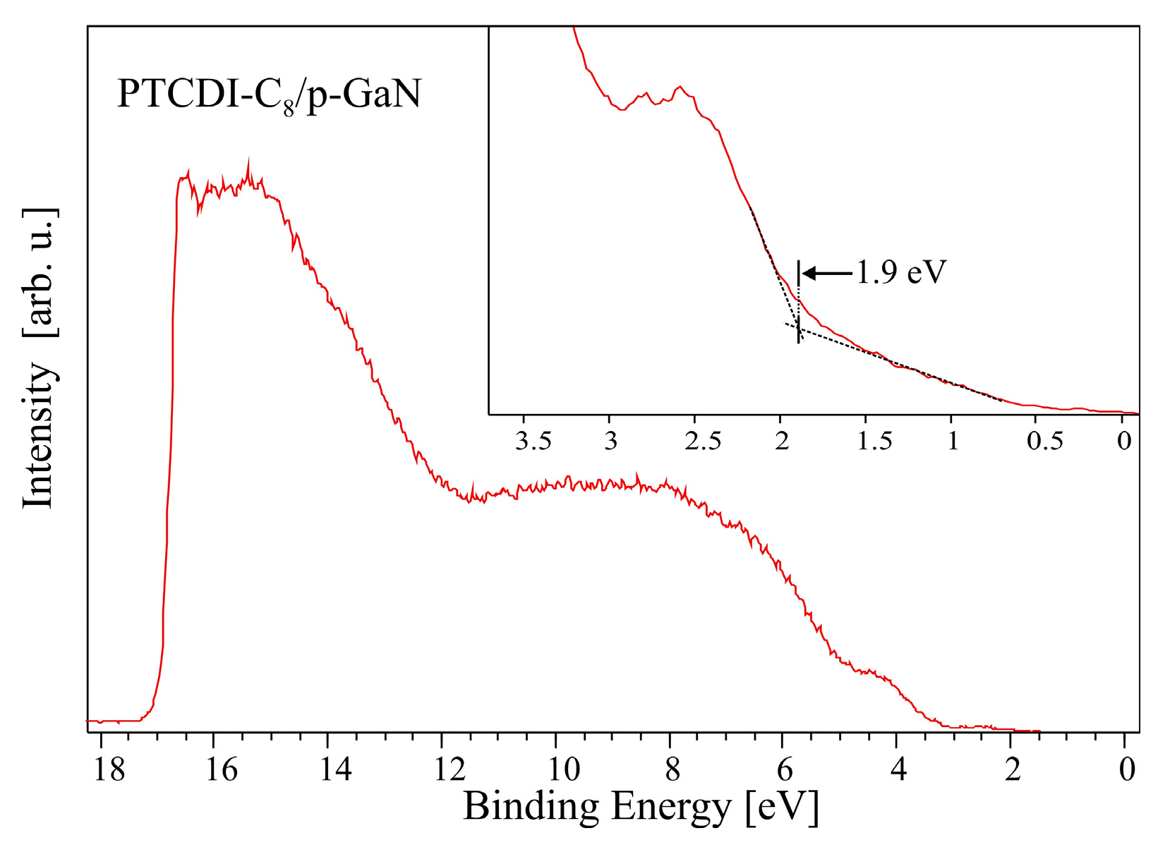
The 5.5 nm thick films have the same work function value, 4.2 eV, independent of the substrate type (n- or p-) onto which the film was deposited. The only difference in the electronic structure of the PTCDI-C8 films concerns their HOMO level position. In the case of the film on p-GaN, its level is situated 0.3 eV closer to the Fermi level than for the film on n-GaN. This shift of the HOMO level of the PTCDI-C8 film on p-GaN is caused, most probably, by the same surface states which are responsible for strong band bending at the subsurface region of p-GaN.
There were no positive results of our STM studies regarding the adsorption of single PTCDI-C8 molecules on the GaN(0001) surface. STM topographies of the surface after the first dose of deposition are blurred, indicating that the adsorbate is weakly bounded and the molecules are mobile. In the case of p-GaN, the situation improves when the self-organization of the adsorbate begins and the two-dimensional islands start to grow. In the case of n-GaN, the poor quality of the STM images made STM observations more difficult at least up to the 1.8 nm thick films; the thickest PTCDI-C8 films on n-GaN studied herein using STM. It seems that at the first stages of the growth interaction between PTCDI-C8 molecules and the substrate are weaker on the n-type substrate. This could be caused by stronger rewetting mechanisms, which compete with the 3D growth mechanisms. Rewetting could be strengthened by the larger amount of carbon residue left on the n-type surface after cleaning procedures. The presence of carbon on the surface is the only factor which chemically differentiates the n- and p-GaN substrates.
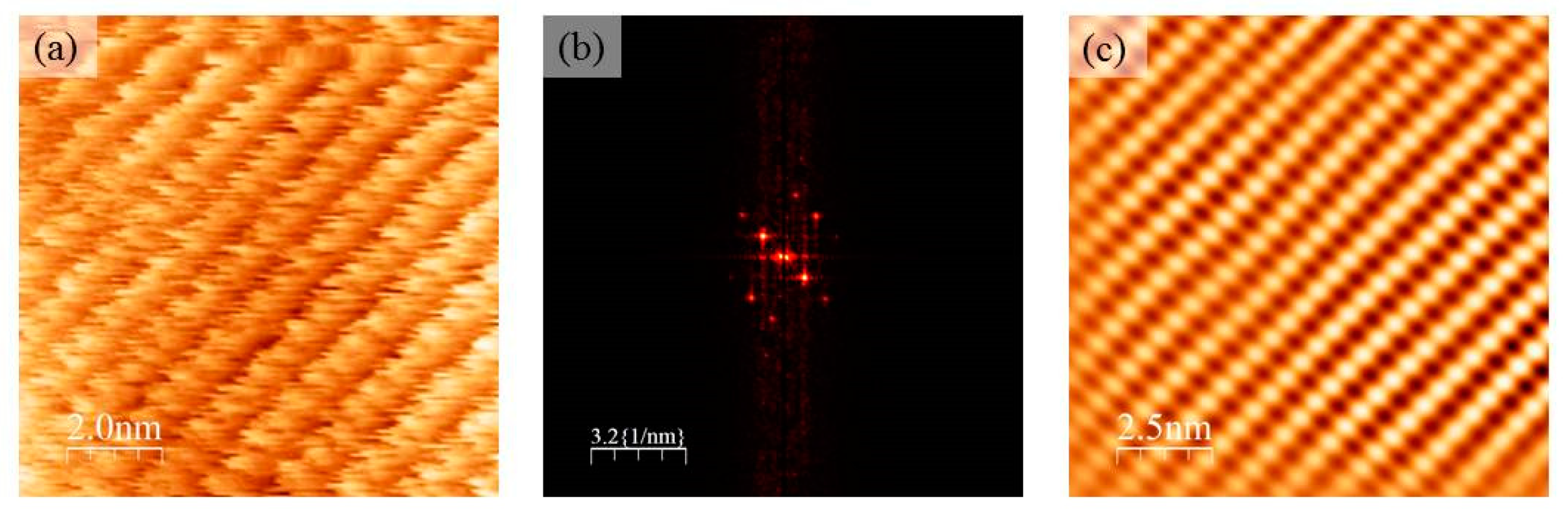
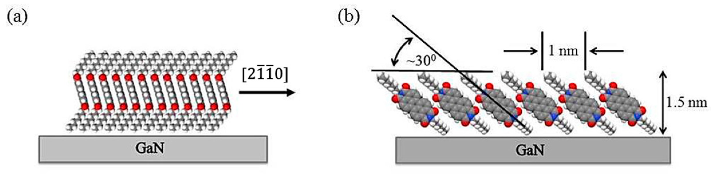
The self-organization of the PTCDI-C8 molecules deposited on p-GaN(0001) begins when the film reaches an average thickness of 0.4 nm, at which the first 2D islands are observed. The islands have an ordered row structure. The analysis of the STM patterns of the films, for this range of thickness, reveals that the molecules in the row are in stand-up positions, as evidenced by the island’s height of 1.5 nm (the thinnest observed), with a linear molecule packing density of 1.7 × 10
7 molecules/cm. This corresponds well with the arrangement of PTCDI-C8 molecules shown in
Figure 12a. Although the dominant factor in self-organization is the interaction between molecules, the substrate structure influences the orientation of the island. The rows are parallel to the closely packed crystallographic directions of the substrate, in this case to [
]. This means that the island’s growth is epitaxial. The structure of the layers constituting the thin films on GaN(0001) surfaces proposed here is schematically shown in
Figure 12. The molecules set in the way shown in
Figure 12a interact through π bonds formed between the cores of the molecules creating the row. Tilted rows stacked one beside another compose the layer as it is shown in
Figure 12b. The height of the layer depends on the tilting angel of the rows. For the layer depicted in
Figure 12b, the tilting angle is equal to ~30°, which makes the layer 1.5 nm high, with the distances between the alkyl tiles of the molecules forming a row equal to 1.0 nm, just like for the PTCDI-C8 layer shown in
Figure 9.
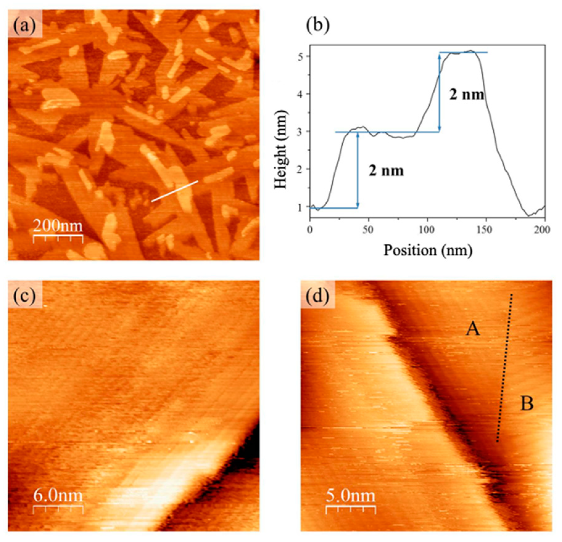
The growth of 2D islands transforms into 3D growth when the average thickness of the film exceeds 1.2 nm. PTCDI-C8 molecules do not form a wetting layer. The substrate is not fully covered by the first layer when the second starts to grow. The increase in the average thickness d of the film results in the growth of consecutive layers of adsorbate on top of the bilayer. Three-layered islands bordering with uncovered by the adsorbate areas of the substrate are observed even for the 5.5 nm thick films. The molecular structure of the second and consecutive monomolecular layers is like the one sketched in
Figure 12. It seems that height of the monomolecular layer increases following the increase in the quantity of the molecules composing the layer. Usually, the bottom layers of the island are thicker than the top one. This may be caused by a change in the tilting angel of the rows or the angle between the core and the alkyl tiles of the molecule. Similar mechanisms of growth and similar results concerning the morphology of the growing films of PTCDI-C8 and PTCDI-C13 were observed on SiO
2 surfaces [
11,
31].
The PTCDI-C8 films on GaN(0001) grow following the Volmer–Weber growth mode. The rewetting mechanisms observed in the PTCDI-C8/GaN(0001) system relax the thermodynamic instabilities in the morphology of the growing or already-grown films. The formation of instabilities is a kinetic effect that depends on growth parameters such as the flux of the deposited molecules or substrate temperature during deposition, as well as the intra- and interlayer surface diffusion controlled by Ehrlich–Schwöbel barriers (ESB). All these factors significantly influence the islands’ nucleation and morphology evolution under conditions far from thermodynamic equilibrium [
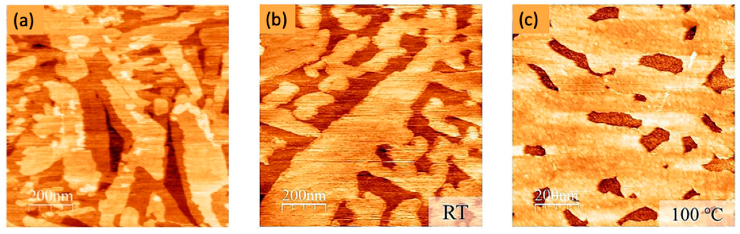
32]. The fundamental molecular building blocks of the PTCDI-C8 films on GaN(0001), produced by self-organization, are molecular rows formed by π–π bonds between the cores of the molecules and the layers assembled into rows by Van der Waals forces. Interactions between the layers constituting the 3D islands is also of a Van der Waals type. Under the growth condition used in this study during film deposition, the supersaturation of the 2D gas of the organic molecules adsorbed on the surface favors the formation of the critical nuclei of monomolecular layers on top of the already existing PTCDI-C8 layers, and as a consequence of the growth of the 3D terraced mounds. The terraces of the PTCDI-C8 mounds are clearly distinguishable from the terraces of the substrate (compare
Figure 1a or
Figure 1b with
Figure 10a). The rewetting observed during the aging at RT or annealing at 100 °C results from the decay of the top-most layers, which are smaller, in the favor the lower ones, which are larger; this is the so-called “Ostwald ripening” [
33]. The rewetting also shows that the ESB is lower for the diffusion of the organic molecule down-step of the terraces of the grown organic mounds than for the diffusion up-step. As observed here, Volmer–Weber growth is a kinetic effect; it seems possible to find such growth conditions as those at which the organic films could grow layer-by-layer, according to the Frank van der Merve growth mode.
5. Conclusions
The chemical composition and electronic structure of the surface and subsurface region, as well as the atomic structure and morphology of the bare n- and p-type GaN(0001) samples were characterized prior to PTCDI-C8 film deposition using XPS, UPS, LEED and STM—the differences between both types of the surfaces used as substrates have been discussed. We did not notice at the measured XPS spectra, any variations in the electronic structure of the substrate or adsorbed molecules due to PTCDI-C8 film growth; therefore, it has been assumed that the film–substrate interaction is of a Van der Waals character. Work function changes have been measured using UPS as a function of the average film thickness. The UPS measurements have allowed us to determine the position of the HOMO level for thicker films with an average thickness 3.2–5.5 nm. Energy diagrams of the interface between the n- and p-type GaN(0001) substates and the PTCDI-C8 films have been proposed. On the basis of STM observations, the fundamental molecular building blocks of the PTCDI-C8 films on GaN(0001), assembled by self-organization, have been identified. The first type of such blocks are rows of PTCDI-C8 molecules stacked in a “stand-up” position in reference to the substrate, supported by the π–π bonds which are formed between the molecular cores of the molecules. The second type are monomolecular layers constituted by rows which are tilted in reference to the layer plane. The layers are epitaxially oriented. The epitaxial relationship between the rows and the crystallographic directions of the substrate has been determined. Assuming that the interaction between the rows and between the layers is also of a Van der Waals forces origin, a model of the PTCDI-C8 film’s growth on the GaN(0001) substrate is presented. The 3D islands of PTCDI-C8 molecules formed on the substrate surface during film deposition are thermodynamically unstable. The Volmer–Weber type of growth observed here is a kinetic effect. Rewetting processes are noticeable after film aging at room temperature or annealing at up to 100 °C.
Anisotropy and the complexity of the interactions inside the PTCDI-C8/GaN(0001) system produce a wide spectrum of basic phenomena, which are of great importance for understanding the growth of organic films on the surfaces of inorganic semiconductors. But there are also practical aspects to such studies. Elements of the organic film’s morphology, such as the structure of the molecular building blocks of the film, its texture, its epitaxial relationship toward the substrate, etc., are key factors that determine its performance in various applications. A proper tuning of the growth parameters allows us to control all these elements; therefore, they may be used as tools for the engineering of hybrid organic–inorganic electronic devices.


 ,
, 