Abstract
In this work, we described the variations in the defect energy levels of four different ZnO morphologies, namely nanoribbons, nanorods, nanoparticles, and nanoshuttles. All the ZnO morphologies were grown on a seeded 4% Boron-doped p-type silicon (p-Si) wafer by using two different synthesis techniques, which are chemical bath deposition and microwave-assisted methods. The defect energy levels were analyzed by using the Deep-Level Transient Spectroscopy (DLTS) characterization method. The DLTS measurements were performed in the 123 K to 423 K temperature range. From the DLTS spectra, we found the presence of different trap-related defects in the synthesized ZnO nanostructures. We labeled all the traps related to the four different ZnO nanostructures as P1, P2, P3, P4, and P5. We discussed the presence of defects by measuring the activation energy (Ea) and capture cross-section (). The lowest number of defect energy levels was exhibited by the ZnO nanorods at 0.27 eV, 0.18 eV, and 0.75 eV. Both the ZnO nanoribbons and nanoparticles show four traps, which have energies of 0.31 eV, 0.23 eV, 0.87 eV, and 0.44 eV and 0.27 eV, 0.22 eV, 0.88 eV, and 0.51 eV, respectively. From the DLTS spectrum of the nanoshuttles, we observe five traps with different activation energies of 0.13 eV, 0.28 eV, 0.25 eV, 0.94 eV, and 0.50 eV. The DLTS analysis revealed that the origin of the nanostructure defect energy levels can be attributed to Zinc vacancies (Vzn), Oxygen vacancies (Vo), Zinc interstitials (Zni), Oxygen interstitials (Oi), and Zinc antisites (Zno). Based on our analysis, the ZnO nanorods showed the lowest number of defect energy levels compared to the other ZnO morphologies.
1. Introduction
Zinc Oxide (ZnO) is one of the most attractive n-type semiconductor materials due to its wide range of optoelectrical and photovoltaic applications. ZnO has a direct wide energy bandgap of 3.37 eV and large excitonic binding energy of about 60 meV at room temperature [1,2]. Its wide bandgap is perfectly suitable for UV-range applications. ZnO is an important semiconductor with unique optical, electrical, electrochemical, mechanical, and thermodynamic properties [3,4,5]. Therefore, ZnO shows strong absorption in the UV region, high transparency to the visible region, high electron mobility, and high conductivity properties [6,7]. ZnO is also widely recognized as a nontoxic, ecofriendly, naturally abundant, cost-effective, and chemically stable material. Among various ZnO structures, hexagonal wurtzite is considered the most stable ZnO structure at ambient conditions with lattice parameters a = b = 0.3250 nm and c = 0.5207 nm [8].
ZnO nanostructures exhibit a wide diversity of morphologies such as nanoparticles, nanowires, nanotubes, nanosprings, nanoplates, nanoflowers, nanobelts, nanorings, nanoshuttles, nanoribbons, nanorods, and nanocages [9,10,11,12,13]. Various nanostructures can be achieved by using different chemicals and different synthesis techniques, including chemical bath deposition (CBD); chemical vapor deposition (CVD); microwave-assisted, sol-gel methods; pulsed laser deposition; magnetron sputtering; spray pyrolysis; carbothermal evaporation; electron beam evaporation; electrochemical growth method; atomic layer deposition; DC-magnetron sputtering; and precipitation methods [9,14,15,16,17,18,19,20,21,22,23,24,25]. Among these techniques, we selected microwave-assisted and chemical bath deposition for this work due to several reasons. Both techniques are simple, cost-effective, and have the ability to uniformly grow reproducible nanostructures. The chemical bath deposition method is a scalable technique that offers uniform growth on large-area substrates. Another advantage is that the chemical bath deposition technique allows for precise control of the properties of nanostructures by changing parameters such as the temperature and deposition time. Microwave-assisted synthesis is a rapidly evolving technique that offers uniform heat distribution, time-saving benefits, and energy efficiency. This method enables control of the temperature, heating rate, and synthesis time. The microwave-assisted technique can be scaled for any industrial application. Based on the fertility of ZnO morphologies and their unique properties, ZnO has been widely employed in different applications in the field of medicine and industry, such as in biosensors, gas sensors, light-emitting diodes, filters, field-effect transistors, transducers, varistors, UV detectors, lasers, solar cells, etc. [26,27,28,29,30,31,32].
In our previous work [9], we investigated the morphological variation of four ZnO morphologies, nanoribbons, nanorods, nanoparticles, and nano shuttles by using Scanning Electron Microscopy (SEM) and Transmission Electron Microscopy (TEM) techniques. The hexagonal structure of four distinct ZnO nanostructures was verified through X-ray Diffraction Spectroscopy (XRD) technology. The crystallinity of ZnO nanoribbons, nanorods, nanoparticles, and nanoshuttles was determined by Different Scanning Calorimetry (DSC). Further, we researched the influence on the optical, electrical, impedance, and wetting properties of four different ZnO nanostructures through UV–visible spectroscopy, Photoluminescence (PL), electrical resistivity, Impedance Spectroscopy, and wettability studies. As an extension of previous studies [33], we focused on the thermoelectric, electrochemical, and dielectric properties of the same four morphologies by using the Seebeck controller technique, Cyclic Voltammetry (CV), Van der Pauw method, and Impedance Spectroscopy. The previous literature discusses the defects of ZnO nanostructures, but few studies have compared the defects of different nanostructured ZnO morphologies (nanoribbons, nanorods, nanoparticles, and nanoshuttles). There is a compelling necessity to conduct research to explicate the variation in the defects present in various ZnO morphologies. This study aims to gain a deeper understanding of the role of defects in different ZnO morphologies, marking a novel investigation that involves the comparison of four distinct morphologies of ZnO.
Defects are considered extremely important parameters in semiconductor devices. Any perturbation of the semiconductor lattice from the ideal structure may be called a defect, which can be either a vacancy, an impurity atom, a self-interstitial defect, or an extended defect [34]. These defects are responsible for the optical, electrical, electrochemical, mechanical, and thermodynamic properties and recombination process, which will affect the efficiency of solar cells and the stability of devices. To improve its functional properties, it is extremely important to identify the defects within each material. There are two types of defects that are intrinsic or native in addition to extrinsic defects. These defect levels are located within the bandgap of a wide-bandgap semiconductor material such as ZnO, TiO2, etc. The ZnO hexagonal close-packed structure has Zn atoms occupying half of the tetrahedral sites, and all the octahedral sites are empty. Therefore, ZnO has more opportunities to affect any perturbation. ZnO intrinsic defect energy levels originate from six main mechanisms [35,36]. The various sites for ZnO to accommodate intrinsic defects are Oxygen vacancies (Vo), Zinc vacancies (Vzn), Oxygen interstitials (Oi), Zinc interstitials (Zni), Zinc antisites (Zno), and Oxygen antisites (Ozn). In this work, the authors mainly focused on investigating, studying, and comparing these ZnO-related intrinsic defect energy levels.
In 1974, the DLTS characterization technique was invented by Lang to characterize semiconductors [37]. DLTS characterization techniques reveal charge traps and help to identify their associated defect states. The DLTS analysis expresses defect energy levels as Ea and (). Due to the complexity of DLTS characterization and instrumentation, there are only a few studies recorded that explore DLTS characterization techniques, compared to those exploring other characterization techniques [38,39,40,41]. To improve the devices with ZnO morphologies, it is necessary to fully understand defect variation with different ZnO morphologies.
The object of this study is to investigate, discuss, and compare the role of all the defect energy levels of four different morphologies, namely nanoribbons, nanorods, nanoparticles, and nanoshuttles. The defect levels were analyzed by using DLTS characterization techniques within the 123 K to 423 K temperature range. We discussed the presence of defects by measuring Ea and . Four different morphologies were synthesized by using two different synthesis techniques, which are chemical bath deposition and microwave-assisted methods. Chemical bath deposition and microwave methods stand out among these techniques due to their simplicity and cost-effectiveness, resulting in uniform growth. The detailed defect analysis from DLTS measurements is described in the results Section 3.
2. Materials and Methods
2.1. Materials
Zinc acetate dehydrate (Zn (CH3COO)2·2H2O, ≥99.5%), Zinc nitrate hexahydrate (Zn (NO3)2·6H2O, ≥99.5%), hexamethylenetetramine (C6H12N4, ≥98%), Sodium hydroxide (NaOH, ≥97%), ammonium hydroxide (NH4OH, 28–30%), Ethyl alcohol (C2H6O, ≥98%), acetic acid (CH3CO2H, ≥99%), and Triton X-100 (t-Oct-C6H4- (OCH2CH2)xOH, x = 9−10) were purchased from Sigma-Aldrich (St. Louis, MI, USA).
2.2. Seed Layer Deposition
The ZnO seed layer was deposited on 4% Boron-doped p-type silicon (p-Si) by using the sputtering technique with a Zinc target. The sputter coater, obtained from SPI Supplies, was operated at 220 V for 45 min. All the seeded samples were annealed for one hour at 300 °C.
2.3. Preparation of ZnO Nanostructues
The ZnO nanoribbons and nanorods were synthesized by using the chemical bath deposition (CBD) method while the ZnO nanoparticles and nanoshuttles were prepared by using a commercial microwave (model no. EM720CGA-PMB). For the fabrication of ZnO nanoribbons, Zinc nitrate hexahydrate (0.1 M) was dissolved in water, stirred for an hour, and ammonium hydroxide was added to achieve a pH of 9. The solution was then utilized to immerse a seeded substrate, subjected to heating at 95 °C for 5 h, followed by annealing at 300 °C for 1 h in an air environment. The ZnO nanorods were prepared by stirring equimolar solutions of Zinc nitrate hexahydrate and hexamethylenetetramine for 2 h, and a seeded substrate was immersed in the resulting solution (pH 7) at 95 °C for 6 h, with subsequent annealing at temperatures of 300 °C in air. The ZnO nanoparticles were synthesized by dissolving Zinc acetate dehydrate (0.1 M) in ethanol, adjusting the pH to 10 with Sodium hydroxide, and subjecting the solution to a 2 min microwave treatment at 210 W. The ZnO nanoparticles were dispersed in a solution containing Triton X-100, acetic acid, and ethanol and deposited a thin film on a substrate, followed by annealing at 300 °C in air. An alternative method for ZnO nanoshuttles involved dissolving Zinc nitrate hexahydrate (0.1 M) in ethanol, adjusting the pH to 9, applying microwave heating for 15 min at 210 W, and subsequent annealing at various temperatures (300 °C) in the air for the synthesized samples.
We carefully adjusted the synthesis temperature, concentration, deposition time, and pH value to reproduce four different morphologies. The synthesis process was repeated multiple times to achieve these four distinct morphologies, which were characterized by using Scanning Electron Microscopy (SEM) and Transmission Electron Microscopy (TEM). A detailed analysis of these four morphologies was previously discussed in our work [9].
In this work, all ZnO morphologies were grown on a seeded 4% Boron-doped p-type silicon (p-Si) to construct the heterojunction, as shown in Figure 1. Finally, all four different ZnO nanostructures were postannealed at 300 °C for 1 h.
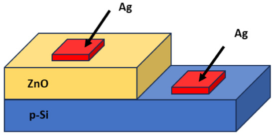
Figure 1.
ZnO/p-Si heterojunction.
2.4. Material Characterization
The defect energy level variation of four different nanostructured ZnO morphologies, namely nanoribbons, nanorods, nanoparticles, and nanoshuttles, were analyzed through the DLTS characterization technique from the 123 K to 423 K temperature range (Zurich Instruments, MFIA, Zürich, Switzerland). By applying a 500 mV fixed bias, deep-level traps in the material are filled with charge carriers. A liquid nitrogen cryostat was used to control the temperature.
3. Results
DLTS Analysis
A DLTS characterization technique was applied to analyze the defect energy levels in the bandgap of the ZnO nanostructures. The majority and minority traps can be observed from the DLTS spectra. Figure 2a–d shows the individual DLTS spectra of the four different ZnO nanostructures, which are nanoribbons, nanorods, nanoparticles, and nanoshuttles. All the measurements were conducted within the 123 K to 423 K temperature range and with a 500 mV DC bias. According to our study, we noted that several defects are introduced and improved the intensity during the higher temperatures. The DLTS signal peaks provide information about the characteristics of these defects of the ZnO nanostructures (the nanoribbons, nanorods, nanoparticles, and nanoshuttles). Figure 3 shows the change in the capacitance of a ZnO/P-Si heterojunction after a pulse is applied. This change in capacitance is related to the capture of charge carriers by deep-level defects within the ZnO nanostructures at specific energy levels within the bandgap. The resulting change in capacitance is recorded as a transient signal, and the peaks in this signal correspond to different energy levels of defects. In this study, all the DLTS spectra revealed the presence of different traps related to different defects in the synthesized nanostructures. We labeled all the traps related to the four different nanostructures as P1, P2, P3, P4, and P5.
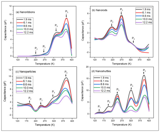
Figure 2.
DLTS spectra of ZnO nanostructures: (a) nanoribbons, (b) nanorods, (c) nanoparticles, and (d) nanoshuttles.
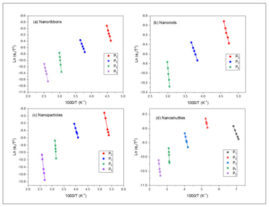
Figure 3.
Arrhenius plots for the traps P1, P2, P3, P4, and P5, observed in the DLTS spectra of ZnO nanostructures: (a) nanoribbons, (b) nanorods, (c) nanoparticles, and (d) nanoshuttles.
According to Figure 2a, the ZnO nanoribbons’ morphology exhibits four different traps, which are labeled as P2, P3, P4, and P5. For the nanorods, we observed three traps, which are indicated as P2, P3, and P4 (Figure 2b). Figure 2c displays the DLTS spectrum of the nanoparticles, consisting of four different traps: P2, P3, P4, and P5. The nanoshuttles exhibit five traps, which are considered as P1, P2, P3, P4, and P5 (Figure 2d). The thermal activation energy of defect states is given by Equation (1):
where A is a constant (), is the trap emission rate, k is Boltzmann’s constant, T is the absolute temperature, is the activation energy, is the capture cross-section, is the effective mass of the electron, and h is Planck’s constant.
A detailed analysis of the parameters corresponding to the nanoribbons, nanorods, nanoparticles, and nanoshuttles is listed in Table 1. The linear fitting of those plots is represented in Equation (2):

Table 1.
Trap energies for nanoribbons, nanorods, nanoparticles, and nanoshuttles.
Arrhenius plots of the traps for each morphology (the nanoribbons, nanorods, nanoparticles, and nanoshuttles) are shown in Figure 3. We analyzed the defect energy levels by using Ea and , which are determined from the Arrhenius plots. By applying a variety of rate windows, the defect parameters can be obtained by using Equation (1) [37].
Before analyzing the DLTS traps, it is important to summarize the background scientific literature data related to the defect levels in ZnO. There are two types of defects, intrinsic and extrinsic, which are exhibited in ZnO [42,43,44]. According to the results of previous studies, several defect energy levels related to ZnO have been investigated, such as Oxygen vacancies (Vo), Zinc vacancies (Vzn), Oxygen interstitials (Oi), Zinc interstitials (Zni), Zinc antisites (Zno), and Oxygen antisites (Ozn) [35,45]. The trap sites created by the defects significantly influence the electrical and optical properties of a semiconductor device [46].
From the scientific literature, we commonly found an electron trap with ∼0.10 eV corresponding to the ZnO crystals [41,47,48,49]. However, this defect level is still not fully accepted as the signature defect in ZnO. Oh et al. reported a defect energy level of 0.065 eV in ZnO synthesized by using a molecular beam epitaxy (MBE) technique [50]. Two activation energy levels of 0.10 eV ( = 3 × ) and 0.11 eV ( = 2 × ) were found in hydrothermally grown ZnO samples similar to our studies [51]. Paradowska et al. also found a defect with an energy of 0.06 ± 0.01 eV in a ZnO base heterojunction, and they claimed that this trap is in the shallow defect level [47]. A shallow donor level of 0.06–0.07 eV was observed in bulk ZnO, which was grown by using a vapor-phase technique [52]. The Zinc antisites (Zno) defect energy level can be located at 0.02 eV below the conduction energy band [53,54]. An appropriate interpretation of this defect energy level is a semishallow donor defect related to Zinc antisites (Zno).
The next widely reported electron trap is the ∼0.2 eV activation energy in ZnO crystals [55]. Bylander et al. theoretically proved that the activation energy at 0.22 eV below the conduction band appears due to the Zinc interstitial (Zni) [55]. According to previous studies, this trap occurs due to the Zinc interstitial (Zni) or the second ionization energy of the native Zinc interstitial donor () [52,56,57]. Around 180 K, Rohatgi et al. also observed a 0.26 eV electron trap, and they claimed that it is related to Zni and most likely [58]. Zinc interstitials are responsible for the migration and annihilation of Zni at the grain boundary interface [59]. In 2009, Fan et al. suggested that the energy level 0.25 ± 0.01 eV is due to the Zinc interstitials (Zni), and this trap level is closely associated with the stability of ZnO varistors [60].
In several scientific literature sources related to ZnO structures, a trap with an activation energy of 0.29–0.30 eV above the valence band has been also reported [39,40,41,49,61]. The origin of ∼0.30 eV is still controversial. Several authors claimed that this trap observed in ZnO crystals is due to Oxygen vacancy (Vo) or intrinsic Zinc vacancy (Vzn)-related defects [39,41,49,62]. However, some studies claimed that a ∼0.30 eV defect level was attributed to the Oxygen vacancies (Vo) [40,63]. On the other hand, some authors claim that the same 0.30 eV activation energy occurs due to the intrinsic Zinc vacancies (Vzn) [43,62]. Zhao et al. observed defect energy levels around 0.24 eV and 0.35 eV in ZnO [46]. They interpreted these two energy levels as relating to intrinsic Zinc interstitials (Zni) and intrinsic Zinc vacancies (Vzn), respectively. Polyakov et al. observed 0.30 eV and 0.55 eV electron traps in undoped ZnO synthesized by a hydrothermal method [64].
However, researchers also have claimed that defect energies between 0.5 eV and 0.9 eV below the conduction energy band occur due to Oxygen vacancies (Vo) in ZnO crystalline samples [65,66,67,68,69]. Chai et al. found a deep donor at 0.83 eV, which occurs due to Oxygen vacancies (Vo) [68]. Allen et al. reported Oxygen vacancy (Vo) defect energies at approximately 0.7 eV [69]. In 2006, Cao et al. reported Oxygen vacancies (V0) at 0.9 eV in ZnO nanoneedles [67]. In 2007, Selim et al. investigated the nature of native defects in ZnO, and their experimental data revealed an Oxygen vacancy (Vo) defect energy level at ∼0.7 eV [66].
Another common trap state with ∼0.40 eV was reported on ZnO-related samples due to Oxygen interstitials (Oi) [47]. This defect energy level occurs due to the interface of a semiconductor and an oxide [70]. A 0.40 eV electron trap was recorded in ZnO crystals grown by chemical vapor transport synthesis [71]. Liu et al. found 0.43 eV and 0.41 eV defect energy levels below the conduction band on a ZnO/Si heterostructure that was grown by metal–organic chemical vapor deposition [72]. ZnO thin films synthesized through pulsed laser deposition showed an electron trap with activation energy equal to 0.37 eV with a capture cross-section of ∼10−15 cm2 [73].
We will contrast and compare our DLTS results with the reported defect levels. This study conducted a DLTS analysis comparing different ZnO morphologies, and Table 1 summarizes trap energies for nanoribbons, nanorods, nanoparticles, and nanoshuttles. In the ZnO nanoribbons, four trap levels were identified. The ZnO nanorods showed three traps along with associated activation energies and capture cross-sections. The ZnO nanoparticles presented four trap levels, while the ZnO nanoshuttles exhibited five trap energy levels. Figure 4 summarizes the defect levels in various ZnO nanostructures (nanoribbons, nanorods, nanoparticles, and nanoshuttles) based on the DLTS analysis. All the defect energy levels are represented for the conduction band (EC) and the valance band (EV). Figure 4 shows that all the defect energy levels are considerably changed with the ZnO morphology. It can also lead us to control and tune the defect energy levels by modifying the ZnO morphologies.
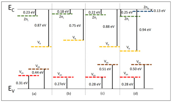
Figure 4.
Defect energy levels of ZnO nanostructures (a) nanoribbons, (b) nanorods, (c) nanoparticles, and (d) nanoshuttles corresponding to DLTS analysis.
In this work, we found that several intrinsic defects exist in the n-ZnO/P-Si heterojunction. All the observed electron trap values are consistent with the values of defect levels reported in the scientific literature data. In all the ZnO morphologies, P2, P2, and P4 electron traps were commonly observed. The P5 electron trap is prominent in the ZnO nanoribbons, nanoparticles, and nanoshuttles. The P1 trap around 0.13 eV is only observed in the ZnO nanoshuttles morphology. According to the literature [47], this 0.13 eV defect energy level trap may occur due to semishallow donor defects related to Zinc antisites (Zno). From previous studies [43,62], the P2 trap with a defect energy level around 0.27 eV to 0.31 eV may be attributed to Zinc vacancies (Vzn). The P3 donor trap appears around 0.18 eV to 0.25 eV below the conduction band and is due to Zinc interstitials (Zni) [55]. The origin of the P4 trap in ZnO is still controversial. According to the literature [65,67], we assume that the defect energy level around 0.75 eV to 0.94 eV is most likely due to Oxygen vacancies (Vo). Therefore, a proper interpretation of the origin of the P5 trap is Oxygen interstitials (Oi) [74].
By contrasting and comparing our DLTS results with the reported defect levels [43,47,55,62,65,67,74], the authors conclude that the origins of all the synthesized ZnO nanostructure’s P1, P2, P3, P4, and P5 defects are Zinc antisites (Zno), Zinc vacancies (Vzn), Zinc interstitials (Zni), Oxygen vacancies (Vo), and Oxygen interstitials (Oi), respectively. However, we did not identify any defect energy levels related to Oxygen antisites (Ozn). The lowest number of defect levels were obtained by the nanorods while the nanoshuttles showed the highest number of defect energy levels compared to the synthesized ZnO nanostructures.
4. Discussion
This study discusses the behavior of the defect energy levels of four ZnO morphologies, which are nanoribbons, nanorods, nanoparticles, and nanoshuttles. Defect engineering is the most useful parameter to tune the charge carrier efficiency and light harvesting. The defect energy levels of different ZnO-morphologies-based heterojunction devices were successfully characterized by using the DLTS technique. We identified the variation in the defect energy levels in all the ZnO morphologies (the nanoribbons, nanorods, nanoparticles, and nanoshuttles) from 123 K to 423 K. We also noted that the presence of defects is considerably changed concerning the ZnO morphology and temperature. The DLTS analysis indicates that the identified defect energy levels are associated with Zinc vacancies (Vzn), Oxygen vacancies (Vo), Zinc interstitials (Zni), Oxygen interstitials (Oi), and Zinc antisites (Zno), which are consistent with the previous literature. However, in this work, we did not find any ZnO defect energy level related to Oxygen antisites (Ozn). The capture cross-section represents the efficiency with which defects in a semiconductor trap charge are carried. We noticed that the capture cross-sections of the observed defects changed significantly. Morphological variations, quantum confinement, and growth conditions might be engineered to favor the formation of defects with different capture cross-sections. We noted that the defect levels significantly changed to a nanostructure morphology. It is necessary to identify the relationship between defect energy levels and photocatalytic activities. We found that the defect energy levels can be controlled with the morphology of the ZnO nanostructures. This may be attributed to the size of each nanostructure, the grain boundary properties, as well as the crystalline quality of the prepared samples. This means that we can control the defect energy levels and associated charge mobilities by changing the ZnO morphology.
In our previous work, we found that the highest crystallinity was obtained by the nanorods compared to the other three morphologies (the nanoribbons, nanoparticles, and nanoshuttles) [9]. This could be one of the main reasons for a reduction in the number of defect levels in the nanorods. The other three morphologies showed low crystallinity. This reduction in crystallinity may affect the defect energy levels in other morphologies. One of the other significant factors is the formation of the Oxygen interstitial defect level in the ZnO nanoribbons, nanoparticles, and nanoshuttles. These Oxygen interstitials mainly influence the conduction process and reduce the mobility of charge carriers [62]. In our previous work, we observed that the ZnO nanorods have the lowest resistivity as well as the lowest real impedance value compared to the nanoribbons, nanoparticles, and nanoshuttles under the same conditions [9]. The DLTS data are consistent with the electrical transport properties of nanorods. Because the nanorods did not show the Oxygen interstitial defect energy level and did show the minimum number of defect energy levels, this may be attributed to the higher electron mobility in the ZnO nanorods. In nanostructured ZnO as well as other materials, particle size also plays an important role in controlling defect engineering. The lower number of defect energy levels in ZnO nanorods may result from the well-crystallized morphology of the rods.
In contrast, the ZnO nanoshuttles showed the highest number of defects at 0.13 eV, 0.28 eV, 0.25 eV, 0.94 eV, and 0.50 eV. These higher defect energy levels may be attributed to increased grain boundary effects, which create a potential barrier for the transport of charge carriers. This may be one of the reasons that the nanoshuttles exhibit the highest electrical resistivity values compared to the nanoribbons, nanorods, and nanoparticles. Overall, we can control the defect energy levels by changing the morphology of ZnO, and ZnO nanorods are the most appropriate morphology compared to nanoribbon, nanoparticle, and nanoshuttle morphologies for photovoltaic and photoelectronic applications due to a relatively low defect environment.
5. Conclusions
In this work, we demonstrated and investigated the defect energy levels in four different ZnO morphologies, namely nanoribbons, nanorods, nanoparticles, and nanoshuttles. The DLTS analysis revealed that the origins of all the synthesized nanostructure defect energy levels are Zinc vacancies (Vzn), Oxygen vacancies (Vo), Zinc interstitials (Zni), Oxygen interstitials (Oi), and Zinc antisites (Zno). In all morphologies, the P2, P3, and P4 electron traps are observed. The P5 electron trap is prominent in the ZnO nanoribbon, nanoparticle, and nanoshuttle morphologies. The lowest number of defect levels of around 0.27 eV, 0.18 eV, and 0.75 eV was observed in the nanorods morphology, whereas the highest number of values of 0.13 eV, 0.28 eV, 0.25 eV, 0.94 eV, and 0.50 eV was observed in the nanoshuttles. Overall, we can tune and control the defect architecture by changing the morphology, and the nanorods show the lowest defect energy levels compared to the other three morphologies: nanoribbons, nanoparticles, and nanoshuttles.
Author Contributions
Conceptualization, P.H., R.R. and G.M.M.; methodology, R.R. and G.M.M.; software, R.R. and G.M.M.; formal analysis, R.R. and G.M.M.; investigation, P.H., R.R. and G.M.M.; data curation, P.H., R.R. and G.M.M.; writing—original draft preparation, R.R.; writing—review and editing, P.H, R.R. and G.M.M.; supervision, P.H.; project administration, P.H.; funding acquisition, P.H. All authors have read and agreed to the published version of the manuscript.
Funding
This research was funded by NASA EPSCoR, grant number 14-2-1205324.
Institutional Review Board Statement
Not applicable.
Informed Consent Statement
Not applicable.
Data Availability Statement
The datasets generated during this study are available from the corresponding author upon reasonable request.
Acknowledgments
The authors are thankful to Rick Portman for helping with the TEM and SEM measurements.
Conflicts of Interest
The authors declare no conflicts of interest.
References
- Willander, M.; Nur, O.; Zhao, Q.; Yang, L.; Lorenz, M.; Cao, B.; Pérez, Z.J.; Czekalla, C.; Zimmermann, G.; Grundmann, M.; et al. Zinc oxide nanorod based photonic devices: Recent progress in growth, light emitting diodes and lasers. Nanotechnology 2009, 20, 332001. [Google Scholar] [CrossRef] [PubMed]
- Özgür, Ü.; Ya, I.; Liu, C.; Teke, A.; Reshchikov, M.; Doğan, S.; Avrutin, V.; Cho, S.-J.; Morkoç, H.A. comprehensive review of ZnO materials and devices. J. Appl. Phys. 2005, 98, 11. [Google Scholar] [CrossRef]
- Jia, Z.; Peng, K.-K.; Li, Y.-H.; Zhu, R.-S. Preparation and photocatalytic performance of porous ZnO microrods loaded with A. Trans. Nonferrous Met. 2012, 22, 873–878. [Google Scholar] [CrossRef]
- Vu Anh, T.; Pham, T.A.T.; Mac, V.H.; Nguyen, T.H. Facile controlling of the physical properties of zinc oxide and its application to enhanced photocatalysis. J. Anal. Chem. 2021, 2021, 5533734. [Google Scholar] [CrossRef] [PubMed]
- Thangeeswari, T.; George, A.T.; Kumar, A.A. Optical properties and FTIR studies of cobalt doped ZnO nanoparticles by simple solution method. Indian J. Sci. Technol. 2016, 9, 4. [Google Scholar] [CrossRef]
- Talam, S.; Karumuri, S.R.; Gunnam, N. Synthesis, characterization, and spectroscopic properties of ZnO nanoparticles. Int. Sch. Res. Not. 2012, 2012, 372505. [Google Scholar] [CrossRef]
- Pathak, T.K.; Kumar, V.; Swart, H.C.; Purohit, L.P. Electrical and optical properties of p-type codoped ZnO thin films prepared by spin coating technique. Phys. E Low Dimens. Syst. Nanostruct. 2016, 77, 1–6. [Google Scholar] [CrossRef]
- Norton, D.P.; Heo, Y.W.; Ivill, M.P.; Ip, K.; Pearton, S.J.; Chisholm, M.F.; Steiner, T. ZnO: Growth, doping & processing. Mater. Today 2004, 7, 34–40. [Google Scholar]
- Rathnasekara, R.; Hari, P. Impedance spectroscopy of nanostructured ZnO morphologies. J. Mater. Res. 2021, 36, 1937–1947. [Google Scholar] [CrossRef]
- Singh, N.; Pandey, P.; Haque, F.Z. Effect of heat and time-period on the growth of ZnO nanorods by sol-gel technique. Optik 2012, 123, 1340–1342. [Google Scholar] [CrossRef]
- Gu, C.; Huang, J.; Wu, Y.; Zhai, M.; Sun, Y.; Liu, J. Preparation of porous flower-like ZnO nanostructures and their gas-sensing property. J. Alloy. Compd. 2011, 509, 4499–4504. [Google Scholar] [CrossRef]
- Yang, F.; Liu, W.-H.; Wang, X.-W.; Zheng, J.; Shi, R.-Y.; Zhao, H.; Yang, H.-Q. Controllable low-temperature vapor-solid growth and hexagonal disk enhanced field emission property of ZnO nanorod arrays and hexagonal nanodisk networks. ACS Appl. Mater. Interfaces 2012, 4, 3852–3859. [Google Scholar] [CrossRef]
- Ding, J.; Fang, X.; Yang, R.; Kan, B.; Li, X.; Yuan, N. Transformation of ZnO polycrystalline sheets into hexagon-like mesocrystalline ZnO rods (tubes) under ultrasonic vibration. Nanoscale Res. Lett 2014, 9, 214. [Google Scholar] [CrossRef]
- Seomoon, K.; Lee, J.; Jang, P.; Jung, C.; Kim, K.-H. Synthesis and characterization of ZnO thin films deposited via PE-MOCVD. Curr. Appl. Phys. 2011, 9, S26–S29. [Google Scholar] [CrossRef]
- Siddiqui, J.; Cagin, E.; Chen, D.; Phillips, J.D. ZnO thin-film transistors with polycrystalline (Ba, Sr) TiO3 gate insulators. Appl. Phys. Lett. 2006, 88, 212903. [Google Scholar] [CrossRef]
- Chen, L.-Y.; Chen, W.-H.; Wang, J.-J.; Hong, F.C.-N.; Su, Y.-K. Hydrogen-doped high conductivity ZnO films deposited by radio-frequency magnetron sputtering. Appl. Phys. Lett. 2004, 85, 5628–5630. [Google Scholar] [CrossRef]
- Chabane, L.; Zebbar, N.; Kechouane, M.; Aida, M.S.; Trari, M. Al-doped and in-doped ZnO thin films in heterojunctions with silicon. Thin Solid Film. 2016, 605, 57–63. [Google Scholar] [CrossRef]
- Arif, M.; Shkir, M.; AlFaify, S.; Ganesh, V.; Sanger, A.; Algarni, H.; Vilarinho, P.M.; Singh, A. A structural, morphological, linear, and nonlinear optical spectroscopic studies of nanostructured Al-doped ZnO thin films: An effect of Al concentrations. J. Mater. Res. 2019, 34, 1309–1317. [Google Scholar] [CrossRef]
- Kawakami, M.; Hartanto, A.B.; Nakata, Y.; Okada, T. Synthesis of ZnO nanorods by nanoparticle assisted pulsed-laser deposition. Jpn. J. Appl. Phys. 2003, 42, L33. [Google Scholar] [CrossRef]
- Prete, P.; Lovergine, N.; Tapfer, L. Nanostructure size evolution during Au-catalysed growth by carbo-thermal evaporation of well-aligned ZnO nanowires on (100) Si. Appl. Phys. A 2007, 88, 21–26. [Google Scholar] [CrossRef]
- Nakanishi, Y.; Miyake, A.; Kominami, H.; Aoki, T.; Hatanaka, Y.; Shimaoka, G. Preparation of ZnO thin films for high-resolution field emission display by electron beam evaporation. Appl. Surf. Sci. 1999, 142, 233–236. [Google Scholar] [CrossRef]
- Liang, J.K.; Su, H.L.; Kuo, C.L.; Kao, S.P.; Cui, J.W.; Wu, Y.C.; Huang, J.C.A. Structural, optical and electrical properties of electrodeposited Sb-doped ZnO nanorod arrays. Electrochim. Acta 2014, 125, 124–132. [Google Scholar] [CrossRef]
- Wang, H.; Xie, J.; Yan, K.; Duan, M. Growth mechanism of different morphologies of ZnO crystals prepared by hydrothermal method. J. Mater. Sci. Technol. 2011, 27, 153–158. [Google Scholar] [CrossRef]
- Miccoli, I.; Spampinato, R.; Marzo, F.; Prete, P.; Lovergine, N. DC-magnetron sputtering of ZnO: Al films on (00.1) Al2O3 substrates from slip-casting sintered ceramic targets. Appl. Surf. Science. 2014, 313, 418–423. [Google Scholar] [CrossRef]
- Htay, M.T.; Hashimoto, Y.; Ito, K. Growth of ZnO submicron single-crystalline platelets, wires, and rods by ultrasonic spray pyrolysis. J. Appl. Phys. 2007, 46, 440. [Google Scholar] [CrossRef]
- Topoglidis, E.; Cass, A.E.G.; O’Regan, B.; Durrant, J.R. Immobilisation and bioelectrochemistry of proteins on nanoporous TiO2 and ZnO films. J. Electroanal. Chem. 2001, 517, 20–27. [Google Scholar] [CrossRef]
- Cheng, X.L.; Zhao, H.; Huo, L.H.; Gao, S.; Zhao, J.G. ZnO nanoparticulate thin film: Preparation, characterization and gas-sensing property. Sens. Actuators B Chem. 2004, 102, 248–252. [Google Scholar] [CrossRef]
- Hames, Y.; Alpaslan, Z.; Kösemen, A.; San, S.E.; Yerli, Y. Electrochemically grown ZnO nanorods for hybrid solar cell applications. Sol. Energy 2010, 84, 426–431. [Google Scholar] [CrossRef]
- Adhyapak, P.V.; Meshram, S.P.; Mulla, I.S.; Pardeshi, S.K.; Amalnerkar, D.P. Materials Science in Semiconductor Processing Controlled synthesis of zinc oxide nanoflowers by succinate-assisted hydrothermal route and their morphology-dependent photocatalytic performance. Mater. Sci. Semicond. Process 2014, 46, 197–206. [Google Scholar] [CrossRef]
- Lenz, T.; Richter, M.; Matt, G.J.; Luechinger, N.A.; Halim, S.C.; Heiss, W.; Brabec, C.J. Charge transport in nanoparticular thin films of zinc oxide and aluminum-doped zinc oxide. J. Mater. Chem. C. 2015, 3, 1468–1472. [Google Scholar] [CrossRef]
- Keis, K.; Bauer, C.; Boschloo, G.; Hagfeldt, A.; Westermark, K.; Rensmo, H.; Siegbahn, H. Nanostructured ZnO electrodes for dye-sensitized solar cell applications. Photochem. Photobiol. A 2002, 148, 57–64. [Google Scholar] [CrossRef]
- Singh, S.; Kumar, Y.; Kumar, H.; Vyas, S.; Periasamy, C.; Chakrabarti, P.; Jit, S.; Park, S.-H. A study of hydrothermally grown ZnO nanorod-based metal-semiconductor-metal UV detectors on glass substrates. Nanomater. Nanotechnol. 2017, 7, 1847980417702144. [Google Scholar] [CrossRef]
- Rathnasekara, R.; Hari, P. Enhancing the Efficiency of Dye-Sensitized Solar Cells (DSSCs) by Nanostructured Ag-doped ZnO Electrodes. ChemistrySelect 2022, 98, e202200830. [Google Scholar] [CrossRef]
- Peaker, A.R.; Markevich, V.P.; Coutinho, J. Tutorial: Junction spectroscopy techniques and deep-level defects in semiconductors. J. Appl. Phys. 2018, 123, 161559. [Google Scholar] [CrossRef]
- Ayoub, I.; Kumar, V.; Abolhassani, R.; Sehgal, R.; Sharma, V.; Sehgal, R.; Swart, H.C.; Mishra, Y.K. Advances in ZnO: Manipulation of defects for enhancing their technological potentials. Nanotechnol. Rev. 2022, 11, 575–619. [Google Scholar] [CrossRef]
- Vanheusden, K.; Seager, C.H.; Warren, W.L.T.; Tallant, D.R.; Voigt, J.A. Correlation between photoluminescence and oxygen vacancies in ZnO phosphors. Appl. Phys. Lett 1996, 68, 403–405. [Google Scholar] [CrossRef]
- Lang, D.V. Deep-level transient spectroscopy: A new method to characterize traps in semiconductors. J. Appl. Phys. 1974, 45, 3023–3032. [Google Scholar] [CrossRef]
- Wenckstern, V.H.; Pickenhain, R.; Schmidt, H.; Brandt, M.; Biehne, G.; Lorenz, M.; Grundmann, M.; Brauer, G. Deep acceptor states in ZnO single crystals. Appl. Phys. Lett. 2006, 89, 092122. [Google Scholar] [CrossRef]
- Simpson, J.C.; Cordaro, J.F. Characterization of deep levels in zinc oxide. J. Appl. Phys. 1988, 63, 1781–1783. [Google Scholar] [CrossRef]
- Auret, F.D.; Goodman, S.A.; Hayes, M.; Legodi, M.J.; Van Laarhoven, H.A.; Look, D.C. Electrical characterization of 1.8 MeV proton-bombarded ZnO. Appl. Phys. Lett. 2001, 79, 3074–3076. [Google Scholar] [CrossRef]
- Auret, F.D.; Nel, J.M.; Hayes, M.; Wu, L.; Wesch, W.; Wendler, E. Electrical characterization of growth-induced defects in bulk-grown ZnO. Superlattices Microstruct. 2006, 39, 17–23. [Google Scholar] [CrossRef]
- Cordaro, J.F.; Shim, Y.; May, J.E. Bulk electron traps in zinc oxide varistors. J. Appl. Phys. 1986, 60, 4186–4190. [Google Scholar] [CrossRef]
- Chiou, B.-S.; Chung, M.-C. Admittance spectroscopy and trapping phenomena of ZnO based varistors. Electron. Mater. 1991, 20, 885–890. [Google Scholar] [CrossRef]
- Blatter, G.; Greuter, F. Electrical Properties of Grain Boundaries in Polycrystalline Compound Ceramics. Semicond. Sci. Technol. 1990, 5, 111–137. [Google Scholar]
- Frenzel, H.; Wenckstern, H.V.; Weber, A.; Schmidt, H.; Biehne, G.; Hochmuth, H.; Lorenz, M.; Grundmann, M. Photocurrent spectroscopy of deep levels in ZnO thin films. Phys. Rev. B 2007, 76, 035214. [Google Scholar] [CrossRef]
- Zhao, X.; Li, J.; Li, H.; Li, S. Intrinsic and extrinsic defect relaxation behavior of ZnO ceramics. J. Appl. Phys. 2012, 111, 124106. [Google Scholar] [CrossRef]
- Paradowska, K.M.; Płaczek-Popko, E.; Pietrzyk, M.A.; Gwóźdź, K. Kozanecki, A. Current transport and deep levels in p-Si/n-Zn0.9Mg0.1O/n-ZnO heterojunction. J. Alloy. Compd. 2017, 691, 946–951. [Google Scholar] [CrossRef]
- Polyakov, A.Y.; Smirnov, N.B.; Govorkov, A.V.; Kozhukhova, E.A.; Belogorokhov, A.I.; Norton, D.P.; Kim, H.S.; Pearton, S.J. Shallow and deep centers in as-grown and annealed MgZnO/ZnO structures with quantum wells. J. Electron. Mater. 2010, 39, 601–607. [Google Scholar] [CrossRef]
- Auret, F.D.; Goodman, S.A.; Legodi, M.J.; Meyer, W.E.; Look, D.C. Electrical characterization of vapor-phase-grown single-crystal ZnO. Appl. Phys. Lett. 2002, 80, 1340–1342. [Google Scholar] [CrossRef]
- Oh, D.C.; Suzuki, T.; Kim, J.J.; Makino, H.; Hanada, T.; Cho, M.W.; Yao, T. Electron-trap centers in ZnO layers grown by molecular-beam epitaxy. Appl. Phys. Lett. 2005, 86, 032909. [Google Scholar] [CrossRef]
- Quemener, V.; Vines, L.; Monakhov, E.V.; Svensson, B.G. Evolution of deep electronic states in ZnO during heat treatment in oxygen-and zinc-rich ambients. Appl. Phys. Lett. 2012, 100, 112108. [Google Scholar] [CrossRef]
- Look, D.C.; Reynolds, D.C.; Sizelove, J.R.; Jones, R.L.; Litton, C.W.; Cantwell, G.; Harsch, W.C. Electrical properties of bulk ZnO. Solid State Commun. 1998, 105, 399–401. [Google Scholar] [CrossRef]
- Vempati, S.; Mitra, J.; Dawson, P. One-step synthesis of ZnO nanosheets: A blue-white fluorophore. Nanoscale Res. Lett. 2012, 7, 470. [Google Scholar] [CrossRef] [PubMed]
- Wen, X.; Zhang, Q.; Shao, Z. Magnetron sputtering for ZnO: Ga scintillation film production and its application research status in nuclear detection. Crystals 2019, 9, 263. [Google Scholar] [CrossRef]
- Bylander, E.G. Surface effects on the low-energy cathodoluminescence of zinc oxide. J. Appl. Phys. 1978, 49, 1188–1195. [Google Scholar] [CrossRef]
- Hagemark, K.I.; Chacka, L.C. Electrical transport properties of Zn doped ZnO. J. Appl. Phys. 1975, 15, 261–270. [Google Scholar] [CrossRef]
- Choi, J.S.; Yo, C.H. Study of the nonstoichiometric composition op zinc oxide. J. Phys. Chem. Solids 1976, 37, 1149–1151. [Google Scholar] [CrossRef]
- Rohatgi, A.; Pang, S.K.; Gupta, T.K.; Straub, W.D. The deep level transient spectroscopy studies of a ZnO varistor as a function of annealing. J. Appl. Phys. 1988, 63, 5375–5379. [Google Scholar] [CrossRef]
- Tapan, K.G.; William, G.C. Barrier voltage and its effect on stability of ZnO varistor. J. Appl. Phys. 1982, 53, 7401–7409. [Google Scholar]
- Fan, J.; Zhang, Z.; Tian, H.; Zhao, H.; Freer, R. Investigation of the effect of different dopants on the trap states of ZnO-based and SnO2-based varistors. J. Phys. Conf. Ser. 2009, 152, 012060. [Google Scholar] [CrossRef]
- Vines, L.; Monakhov, E.V.; Svensson, B.G. Effect of high-temperature treatments on defect centers and impurities in hydrothermally grown ZnO. Phys. B Condens. 2009, 404, 4386–4388. [Google Scholar] [CrossRef]
- Chicot, G.; Pernot, J.; Santailler, J.-L.; Chevalier, C.; Granier, C.; Ferret, P.; Ribeaud, A.; Feuillet, G.; Muret, P. Electronic properties of E3 electron trap in n-type ZnO. Phys. Status Solidi B 2014, 251, 206–210. [Google Scholar] [CrossRef]
- Vehse, W.E.; Sibley, W.A.; Keller, F.J.; Chen, Y. Radiation damage in ZnO single crystals. Phys. Rev. 1968, 167, 828. [Google Scholar] [CrossRef]
- Polyakov, A.Y.; Smirnov, N.B.; Govorkov, A.V.; Kozhukhova, E.A.; Pearton, S.J.; Norton, D.P.; Osinsky, A.; Dabiran, A. Electrical properties of undoped bulk ZnO substrates. J. Electron. Mater. 2006, 35, 663–669. [Google Scholar] [CrossRef]
- Ullattil, S.G.; Jabeen, F.M.J.; Abdel-Wahab, A. Defect minimized Ag-ZnO microneedles for photocatalysis. Environ. Sci. Pollut. Res. 2020, 27, 37036–37043. [Google Scholar] [CrossRef] [PubMed]
- Selim, F.A.; Weber, M.H.; Solodovnikov, D.; Lynn, K.G. Nature of native defects in ZnO. Phys. Rev. Lett. 2007, 8, 085502. [Google Scholar] [CrossRef] [PubMed]
- Cao, B.; Cai, W.; Zeng, H. Temperature-dependent shifts of three emission bands for ZnO nanoneedle arrays. Appl. Phys. Lett. 2006, 88, 161101. [Google Scholar] [CrossRef]
- Chai, J.; Mendelsberg, R.J.; Reeves, R.J.; Kennedy, J.; Von, W.H.; Schmidt, M.; Grundmann, M.; Doyle, K.; Myers, T.H.; Durbin, S.M. Identification of a deep acceptor level in ZnO due to silver doping. J. Electron. Mater. 2010, 39, 577–583. [Google Scholar] [CrossRef]
- Allen, M.W.; Durbin, S.M. Influence of oxygen vacancies on Schottky contacts to ZnO. Appl. Phys. Lett. 2008, 92, 122110. [Google Scholar] [CrossRef]
- Hisham, H. Characterization Methods for Submicron MOSFETs; Springer Science & Business Media: Berlin/Heidelberg, Germany, 2012; Volume 352. [Google Scholar]
- Scheffler, L.; Kolkovsky, V.l.; Lavrov, E.V.; Weber, J. Deep level transient spectroscopy studies of n-type ZnO single crystals grown by different techniques. J. Condens. Matter Phys. 2011, 23, 334208. [Google Scholar] [CrossRef]
- Ci-Hui, L.; Bing-Ce, L.; Zhu-Xi, F. Electrical and deep levels characteristics of ZnO/Si heterostructure by MOCVD deposition. Chin. Phys. B 2008, 17, 2292. [Google Scholar] [CrossRef]
- Von, W.H.; Biehne, G.; Lorenz, M.; Grundmann, M.; Auret, F.D.; Meyer, W.E.; van, R.P.J.J.; Hayes, M.; Nel, J.M. Dependence of trap concentrations in ZnO thin films on annealing conditions. J. Korean Phys. Soc. 2008, 53, 2861–2863. [Google Scholar]
- Wu, X.L.; Siu, G.G.; Fu, C.L.; Ong, H.C. Photoluminescence and cathodoluminescence studies of stoichiometric and oxygen-deficient ZnO films. Appl. Phys. Lett. 2001, 78, 2285–2287. [Google Scholar] [CrossRef]


Disclaimer/Publisher’s Note: The statements, opinions and data contained in all publications are solely those of the individual author(s) and contributor(s) and not of MDPI and/or the editor(s). MDPI and/or the editor(s) disclaim responsibility for any injury to people or property resulting from any ideas, methods, instructions or products referred to in the content. |
© 2024 by the authors. Licensee MDPI, Basel, Switzerland. This article is an open access article distributed under the terms and conditions of the Creative Commons Attribution (CC BY) license (https://creativecommons.org/licenses/by/4.0/).