2. Design and Methods
The polarization-splitting grating coupler was designed on a LNOI platform. The schematic and wave-vector diagram of the GC was shown in
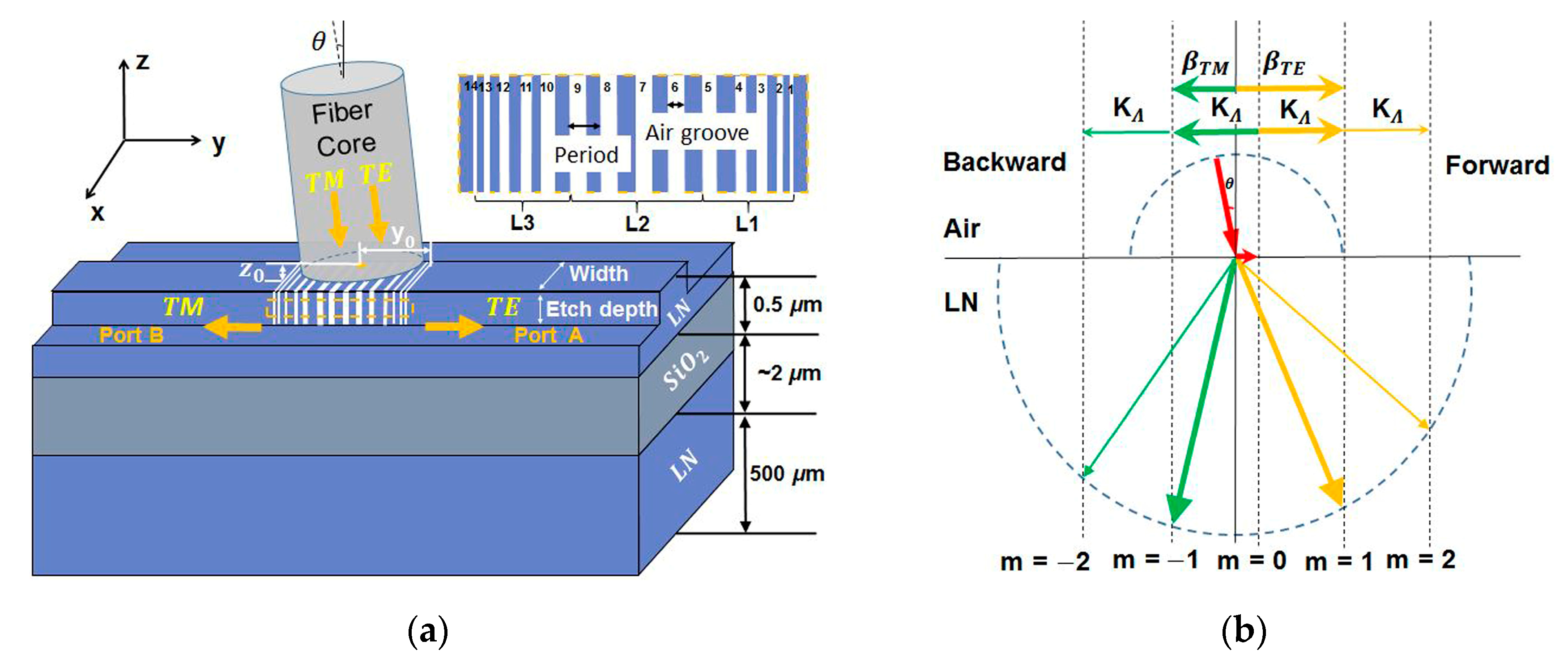
Figure 1.
From bottom to top: lithium niobate (LN) substrate (500 μm), silicon dioxide layer (~2 μm), LN thin film (500 nm), and the single mode fibers (core diameter is 9 μm). Fibers were fixed above the waveguide grating surface at a tilted angle deviated from the z direction. The grating structure was formed by several periodic LN teeth and air grooves which were partially etched in LN thin film waveguide. The vertical position z0 of fiber was defined as the placement from the grating surface, and the horizontal position y0 of fiber was defined as the placement from the first air grove of port A. When light from the single mode fiber is diffracted by the grating, they will be separated into two beams of opposite directions: the forward port A for waveguide TE0 mode, and the backward port B for waveguide TM0 mode.
The polarization-splitting grating is essentially a diffracted Bragg grating. It satisfies the Bragg condition:
where m is the diffraction order,
is the grating vector, and
and
are the wave vectors of the input light and waveguide mode. In y direction, the values
,
, and
.
is the free-space wavelength (
= 1550 nm), Λ is the period of the grating, N
cladding is the refractive index of the top layer on LN (N
cladding = 1), θ is the fiber tilted angle with respect to the normal direction of waveguide surface. N
eff denotes the effective index of waveguide mode, and is different for waveguide TE
0 mode and TM
0 mode, meaning that grating couplers are generally polarization-dependent. The polarization dependence can be employed in splitting the different polarization modes. As schematically shown in
Figure 1b, the grating diffracted the fiber mode to the waveguide TE mode in the forward direction with m = 1 but diffracted the fiber mode to the waveguide TM mode in the backward direction with m = −1. This difference introduced an offset of
for the two modes according to Equation (1), so a grating coupler which can split the TE
0 polarization mode and TM
0 mode in opposite directions was worked out with the initial fiber angle
and
.
denote the refractive indices of waveguide TE
0 and TM
0 modes.
Lumerical mode solutions were employed to find the fundamental TE
0 and TM
0 modes by solving Maxwell’s equations on a cross-section mesh, and the finite different algorithm was used for meshing the structure. Maxwell’s equations were then formulated into a matrix eigenvalue problem, so the effective indices
and
and the mode profile of the two polarization modes could be gained after solving. Finite-difference time-domain simulation method (FDTD) was employed in the grating coupler’s design, simulation, and optimization. To save simulation time, two-dimensional FDTD was applied instead of three-dimensional FDTD, as the typical waveguide width (~12 μm) is much bigger than its height (0.5 μm) [
2]. Perfectly matched layer (PML) boundary conditions were applied to absorb the electromagnetic energy incident to the boundary to avoid interference with the fields inside. FDTD solutions generated a rectangular, Cartesian-style mesh. A lower mesh accuracy of 2 with 10 mesh points per wavelength was employed in the initial optimization for quick optimization, and a higher mesh accuracy of 4 with 18 mesh points per wavelength was employed for the convergency test. Monitors were placed in all sides of the grating, so the upward optical power, the downward optical power, the forward optical power, and the backward optical power could be detected and analyzed. By exploiting the Fourier transforms, normalized transmission and CE were gained.
In simulation, the ordinary and extraordinary refractive indices of LN were set to be 2.2112 and 2.138, and the refractive index of silicon dioxide was set to be 1.46 [
29,
30]. Firstly, a uniform grating coupler for coupling both TE
0 and TM
0 polarization modes was designed and optimized to gain optimal parameters such as period, filling factor, and fiber position. Secondly, the optimal uniform GC was segmented into three parts of which the period and filling factor were modulated to achieve better CEs. Lastly, the fabrication tolerance of parameters was systematically simulated and analyzed.
3. Results and Discussion
The initial optimizations were performed in uniform grating coupler with the calculated θ of 6° and period of 823 nm for both waveguide TE
0 and TM
0 modes by Bragg condition, respectively. Parameters such as Λ, etch depth (d), filling factor (the ratio of the air groove width to the period, FF), θ, and fiber position (y
0 and z
0) were all variables, and were optimized and studied to achieve a good CE and polarization splitting. The relative position of fiber and grating was crucial to the coupling because it played an important role in the diffracted power distribution and mode-matching situation. For the sake of simplicity, z
0 was fixed at 10.1
. The CEs of TE
0 and TM
0 modes with different fiber horizontal position at wavelength 1550 nm were shown in
Figure 2. Different numbers of grating period
N were employed in the optimization. CEs of waveguide TE
0 mode and TM
0 were demonstrated in dashed and solid curves, respectively.
From
Figure 2, the maximum CE of TE
0 and TM
0 modes increased slightly with the increase of N, and the maximum CEs are −3 dB and −4 dB when
,
,
, but a different y
0, respectively. The y
0 corresponding to the peak CE was defined as y
0m. The bigger the N, the bigger the y
0m difference of the two modes. For TE mode, the y
0m varies little (around
, but for TM
0 mode, the y
0m varied widely (from
to
. This might be because that the horizontal position of the first air groove for TM
0 mode was greatly dependent on the N. The optimal y
0m tended to keep close to their own first air groove of TE
0 mode (Port A) and TM
0 mode (Port B), respectively. So, N and y
0m should be properly adjusted to keep an identical grating configuration for both TE
0 and TM
0 modes at the expense of CE. As shown in
Figure 2, the best CE for both TE
0 and TM
0 mode was about −4.2 dB when y
0m = −6.8 µm and N = 9 (red arrow). The CE decreased with the increase of N, dropping to −8.3 dB when N = 21 (black arrow) and y
0m = −11.8 µm. When considering improving the CE and lowering the backward transmission, the next optimizations were performed at a compromise of N = 13 with a CE of −4.82 dB for the two modes.
By diffracting, a uniform grating coupler might yield an exponentially decaying power field distribution along the y direction, so there existed a certain mode mismatch between the input mode field and the waveguide modes field. The CE could be further improved by chirping the period and apodizing the filling factor to form a better mode matching with the waveguide mode. Regarding the basics of uniform grating, the grating region was segmented into three parts named L
1, L
2, and L
3 regions (
Figure 1a). L
1 region, which contained five grating teeth and air grooves numbered 1–5, were chirped and apodized for the mode-matching of waveguide TE
0 mode. L
2 region, which contained a uniform configuration which had four uniform grating teeth and air grooves numbered 6–9, was designed to guarantee coupling strength. L
3 region, which contained four grating teeth and five air grooves numbered 10–14, were apodized for the mode-matching of waveguide TM
0 modes. The dimensions of each grating period and groove width is shown in
Table 1.
As shown in
Table 1, the Λ and groove width in L
1 and L
3 part were varied. In L
1, the parameters of period and filling factor gradually increased from 1–5 for TE
0. Also, the variation of filling factor (
) and variation of period (
) were 0.07 and 19 nm, respectively. In L
3, the filling factor was gradually decreased from 10–14, and
was 0.07. The gradually increased or decreased groove width in L
1 and L
3 regions modified the exponentially decayed power distribution to a Gaussian-like field distribution. The CE for both TE
0 and TM
0 modes could be improved due to the improved mode field matching between the grating diffraction field distribution and waveguide modes field distribution. The details of the chirped and apodized GC could be seen in our primary work [
31]. In addition, the asymmetric configuration of L
1 and L
3 was to reduce the opposite transmission. The peak CEs for TE
0 and TM
0 modes with wavelength are shown in
Figure 3.
It could be seen that CEs of TE0 and TM0 modes were improved to −2.83 dB and −2.82 dB with 3-dB-bandwidths of 73 nm and 100 nm at wavelength 1550 nm, respectively. An increase of about 2 dB in CE was gained when the segmented and apodized grating configuration was applied. The polarization-splitting ratio was defined as the CE of TE0 polarization over the CE of TM0 polarization. The difference of CEs for the two modes was small, indicating that the polarization-splitting GC had a good polarization independence and a good polarization-splitting ratio of 1:1. Along with that, if the gratings numbered 1 and 14 were deleted on consideration of the fabrication process, a decrease of only 0.02 dB was introduced in the CE.
Grating parameters such as the thickness of LN film (h),
, FF, and d played import roles in the CE and splitting ability. Their fabrication tolerances were import to the performance of coupler. CEs at different parameters’ deviations for TE
0 and TM
0 modes were shown in
Figure 4. The CEs of TE
0 mode and TM
0 mode were demonstrated in dashed and solid curves, respectively. The optimal CE at wavelength 1550 nm was marked by an orange dot.
In
Figure 4a, grating period varied around the optimal value of 920 nm with
when other parameters were kept at their optimal values. The red, orange, blue, and black lines denoted the CEs when the periods were 900 nm (
), 910 nm (
), 930 nm (
), and 940 nm (
). A deviation of period made the peak wavelength move, with the greater the deviation of period, the greater the peak wavelength shift. The shift made the intersection point of the two CE curves (TE
0 and TM
0) at the same period move down or move out of the range 1500 nm to 1600 nm. Deviations of
and
introduced decreases of about 0.2 dB and 0.28 dB in CEs, respectively. Deviations of
and
made the intersection point move out of the 1500 nm to 1600 nm range. Therefore, it was difficult to keep the polarization-splitting ratio at 1:1 with a good CE. In addition, at a wavelength of 1550 nm, the CEs for TE
0 and TM
0 modes were −4.4 dB/−3.62 dB, −2.84 dB/−3.06 dB, −3.21 dB/−2.89 dB, and −3.34 dB/−4.32 dB when the periods were set to 900 nm, 910 nm, 930 nm, and 940 nm and the polarization-splitting ratios were 1:1.19, 1:0.95, 1:1.08, and 1:0.8, respectively. The greater the deviation from 1:1, the worse the polarization independence at wavelength 1550 nm of the coupler. It could be seen that deviations of
introduced a maximum extra loss of about 1.6 dB and 1.5 dB for TE
0 and TM
0 modes at wavelength 1550 nm. The above results suggested that the polarization-splitting GC was sensitive to the parameter of grating period which determined the coupling strength. One can vary this parameter to change the CE and polarization-splitting ratio. The deviation of period should be tightly controlled to achieve a good polarization-splitting ratio and CE.
In
Figure 4b, the etch depth varied around the optimal value of 300 nm with
when other parameters were kept at their optimal values. The red, orange, blue, and black lines denote the CEs when the etch depths d were 280 nm (
), 290 nm (
), 310 nm (
), and 320 nm (
), respectively. A deviation of d made the peak wavelength move, a positive deviation resulted in a blue-shift, and a negative deviation resulted in a red-shift for both modes. The greater the deviation of d, the greater the peak wavelength shift. Although parts of the peak CEs increased (the black and blue curves for TE
0 mode), the shift also made the intersection point of the two CE curves (TE
0 and TM
0) at the same etch depth move down. Deviations of
and
resulted in a decrease of CE at intersection points less than 0.1 dB and 0.8 dB, respectively. At a wavelength of 1550 nm, the CEs for TE
0 and TM
0 modes were −3.42 dB/−2.9 dB, −3.02 dB/−2.86 dB, −2.72 dB/−2.83 dB, and −2.82 dB/−2.96 dB when the h was 280 nm, 290 nm, 310 nm, and 320 nm, meaning that the polarization-splitting ratios were 1:1.23, 1:1.04, 1:0.98, and 1:1.03, respectively. Deviations of
only introduced a maximum extra loss about 0.37 dB and 0.13 dB for TE
0 and TM
0 modes at wavelength 1550 nm. The above results suggested that the polarization-splitting GC had a good fabrication tolerance of etching depth. A deviation of
was acceptable.
In
Figure 4c, the h varied around the optimal value of 500 nm with
when other parameters were kept at their optimal values. The red, orange, blue, and black lines denote the CEs when the h was 460 nm (
), 480 nm (
), 520 nm (
), and 540 nm (
), respectively. A deviation of h made the peak wavelength move, a positive deviation resulted in a red-shift, and a negative deviation resulted in a blue-shift for the two modes. The greater the deviation of h, the greater the peak wavelength shift. The shift made the intersection point of the two CE curves (TE
0 and TM
0) at the same h move down or move out of the range 1500 nm to 1600 nm. Deviations of
and
resulted in a decrease of CE at intersection point about 0.34 dB and 0.15 dB, respectively. In addition, at a wavelength of 1550 nm, the CEs for TE
0 and TM
0 modes were −6 dB/−4.2 dB, −3.16 dB/−3.17 dB, −3.59 dB/−2.92 dB, and −5.1 dB/−3.42 dB when the h was 460 nm, 480 nm, 520 nm, and 540 nm, so the polarization-splitting ratio were 1:1.52, 1:1.002, 1:1.17, and 1:1.47, respectively. Deviations of
introduced a maximum extra loss of about 0.76 dB and 0.34 dB for TE
0 and TM
0 modes at wavelength 1550 nm, respectively. Deviations of
introduced a maximum extra loss of about 3.2 dB and 2.3 dB for TE
0 and TM
0 modes at wavelength 1550 nm. The polarization-splitting GC was sensitive to the parameter h which could change the refractive indexes of the waveguide mode. To keep a good CE and polarization-splitting ratio, the deviation of h should be controlled in
.
In
Figure 4d, the filling factor varied around the optimal value of 0.4 with
when other parameters were kept at their optimal values. The red, orange, blue, and black lines denote the CEs when the FF was 0.36 (
), 0.38 (
), 0.42 (
), and 0.44 (
). A deviation of the FF makes the peak wavelength move. A positive deviation results in a blue-shift, and a negative deviation results in a red-shift for both modes. The greater the deviation of FF, the greater the peak wavelength shift. Although parts of the peak CEs were increased (the blue curve for TE
0 mode), the shift also made the intersection point of the two CE curves (TE
0 and TM
0) at the same FF move down. Deviations of
resulted in a decrease of CE at interaction point less than 0.07 dB and 0.7 dB, respectively. It indicated that a CE of −2.91 dB for the two modes with a polarization-splitting ratio of 1:1 was obtained when the deviation was controlled in
. At wavelength 1550 nm, the CEs for TE
0 and TM
0 modes were −3.36 dB/−3.1 dB, −3.02 dB/−2.9 dB, −2.91 dB/−2.8 dB, and −2.97 dB/−3.14 dB when the FF was 0.36, 0.38, 0.42, and 0.44, so the polarization-splitting ratios were 1:1.06, 1:1.03, 1:1.03, and 1:0.96, respectively. Since a narrow FF range near 0.4 was investigated, the polarization-splitting GC showed less-insensitivity to the FF which played an important role in the field distribution. A deviation of
was acceptable.
For the segmented, chirped, and apodized GC,
and
were especially important for the coupling and splitting performance.
Figure 5a,b gave the CEs at different
and
for TE
0 and TM
0 modes. The CEs of TE
0 mode and TM
0 mode were demonstrated in dashed and solid curves. The optimal CE at wavelength 1550 nm was marked by an orange dot.
In
Figure 5a, the red, orange, blue, and black lines denoted the CEs when
were 9 nm (
), 14 nm (
), 24 (
), and 29 (
). Deviations of
made the peak wavelength move. The greater the deviation of
, the greater the peak wavelength shift. The shift made the intersection point of the two CE curves (TE
0 and TM
0) at the same period move down when
were 9 nm and 14 nm, while out of the range from 1500 nm to 1600 nm when
were 24 nm and 29 nm. The decreased CE at the intersection points were −3.05 dB and −2.9 dB when
were 9 nm and 14 nm. This resulted in an extra loss of 0.2 dB and 0.17 dB in CE for the two modes from the optimal value of −2.83 dB, respectively. There was no intersection when
were at 24 nm and 29 nm, as a splitting ratio of 1:1 would never be achieved in that case. At wavelength 1550 nm, the CEs for TE
0 and TM
0 modes were −3.61 dB/−3.05 dB, −2.83 dB/−2.83 dB, −3.44 dB/−2.79 dB, and −3.82 dB/−2.8 dB when
were 9 nm, 14 nm, 24 nm, and 29 nm. The polarization-splitting ratios were 1:1.14, 1:1, 1:1.16, and 1:1.26, respectively. Deviations of
introduced a maximum extra loss of about 1 dB and 0.2 dB for TE
0 and TM
0 modes at wavelength 1550 nm. The worse splitting ratio was obtained when a positive deviation of
which resulted in smaller periods and groove widths in L
1 and L
3 region and could not modify the exponentially decaying distribution of field very well in a limited number of periods was applied.
In
Figure 5b, the red, orange, blue, and black lines denoted the CEs when
were 0.03 (
), 0.04 (
), 0.05 (
), and 0.06 (
), respectively. A deviation of
made the peak wavelength move. A positive deviation resulted in a blue-shift, and a negative deviation resulted in a red-shift for both modes. The greater the deviation of
, the greater the peak wavelength shift. The shift made the intersection points of the two CE curves all move out of the wavelength range from 1500 nm to 1600 nm. It indicated that a splitting ratio of 1:1 would never be obtained when
was deviated from 0.07. At wavelength 1550 nm, the CEs for TE
0 and TM
0 modes were −3.61 dB/−3.05 dB, −2.83 dB/−2.83 dB, −3.44 dB/−2.79 dB, and −3.82 dB/−2.8 dB when
were 9 nm, 14 nm, 24 nm, and 29 nm, and the polarization-splitting ratio were 1:1.14, 1:1, 1:1.16, and 1:1.26, respectively. The polarization-splitting GC was highly sensitive to the parameter of
which was crucial to the modified field distribution. The parameter
should be under precise control since a small deviation of
could destroy the mode field matching condition.
The impact of a deviation of the optimal fiber angle of
on the CE and polarization-splitting ability was also studied. CE at different fiber angles was shown in
Figure 6. The red and black lines denoted the TE
0 and TM
0 modes, respectively. For TE
0 mode, the deviation of fiber angle made the peak wavelength move, a positive deviation resulted in a blue-shift, and a negative deviation resulted in a red-shift. The shift was exactly the opposite for TM
0 mode. A positive deviation resulted in a red-shift, and a negative deviation resulted in a blue-shift. The opposite shift of the two modes made polarization-splitting with a high CE much more difficult. For the two modes, the greater the deviation of fiber angle, the greater the peak wavelength shift. Take θ = 9° for example—the peak wavelength shifts to 1529 nm and 1576 nm for TE
0 and TM
0 modes, respectively. The deviation of
introduced a shift of 47 nm in peak wavelength. Deviation of fiber angle also resulted in change of peak CE. Except for θ = 5°, the peak CEs all decreased with the deviation, and the bigger deviation of fiber angle, the bigger decrease of peak CE. As shown in
Figure 4, the CE at intersection wavelength for both TE
0 and TM
0 mode had a decrease of about 1 dB when the angle deviation equaled to ±3°, respectively. The fiber angle played an important role in polarization splitting and CE, and the deviation should be controlled in ±3° to achieve a good polarization splitting and CE.
The polarization-splitting grating coupler can also be used as polarization beam combiner in the output coupling.
Figure 7 gave the E
x-field profile when used as an output coupler. Waveguide TE
0 and TM
0 modes were excited at port A and port B simultaneously, and were both diffracted by the grating and then combined with the upper fiber. The total transmission was −2.72 dB, which contained 45% TE
0 and 55% TM
0 polarization. The ratio of TE
0 and TM
0 polarization was about 1:1.22, which is a decrease from the polarization-splitting ratio of 1:1. This might be attributed to the interaction of the two beams in the output coupling which did not happen in the input coupling. At the input coupling, TE
0 and TM
0 polarization lights were employed separately, but were excited simultaneously at the output coupling.


