
Mechanical Response of Cu/Sn58Bi-xNi/Cu Micro Solder Joint with High Temperatures

Abstract
:1. Introduction
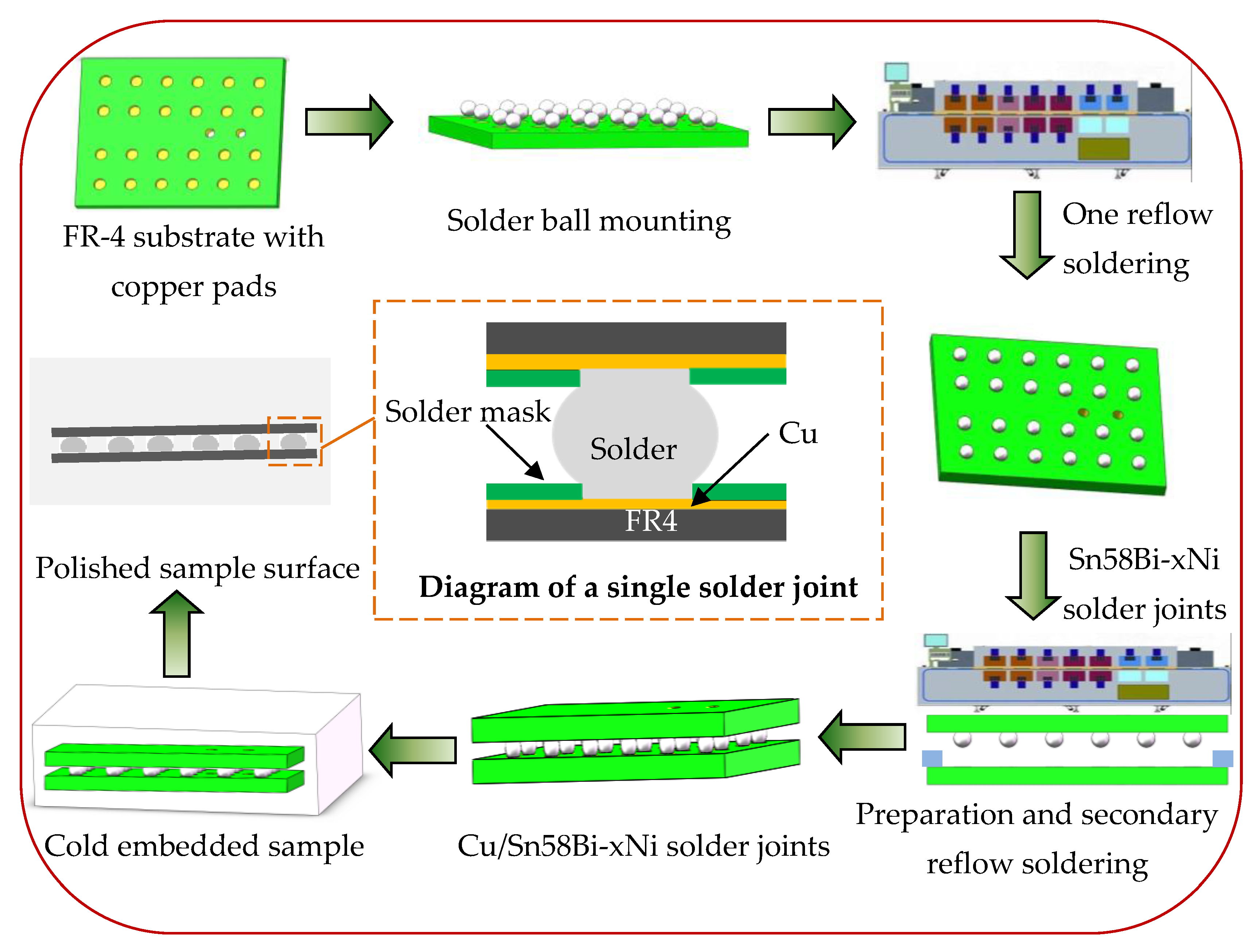
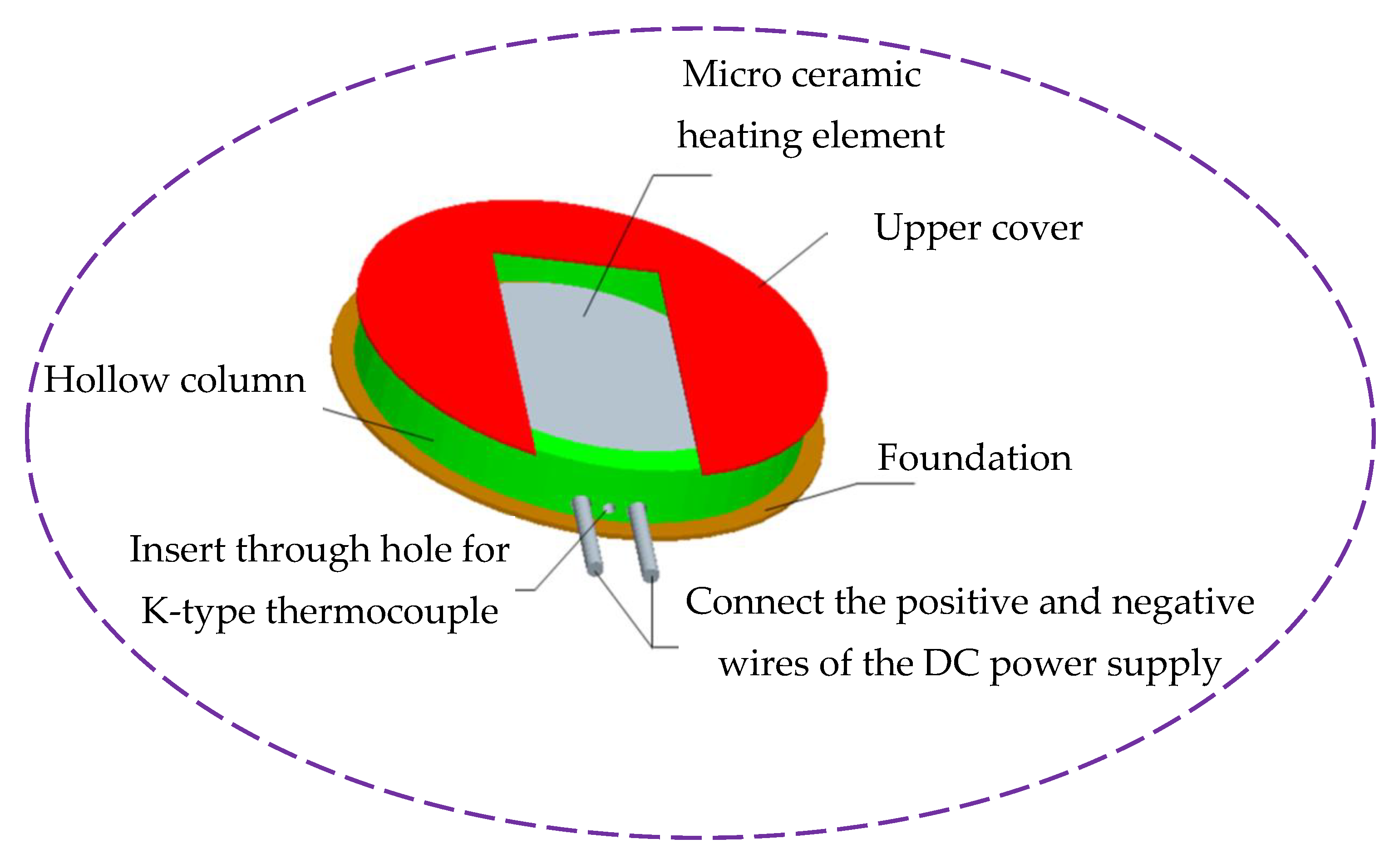
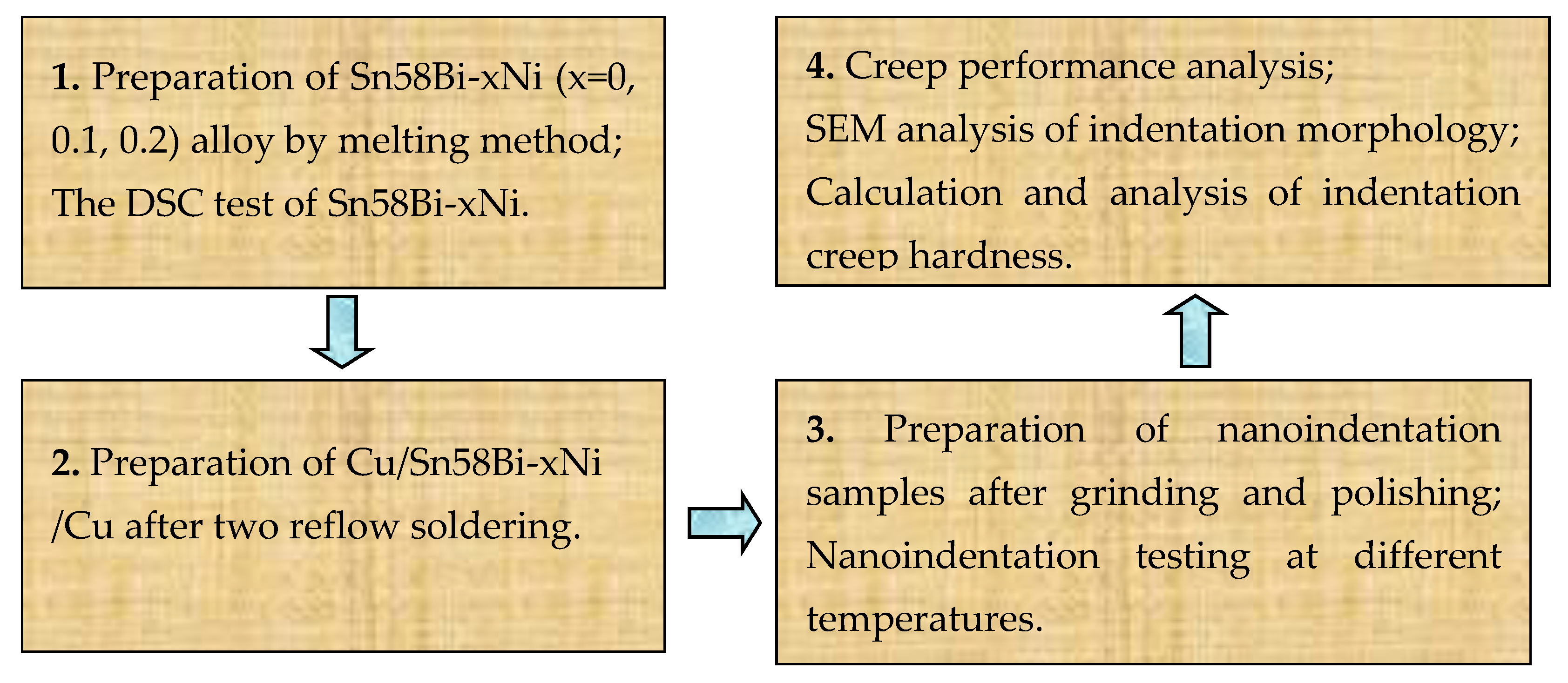
2. Materials and Methods
3. Results and Discussion
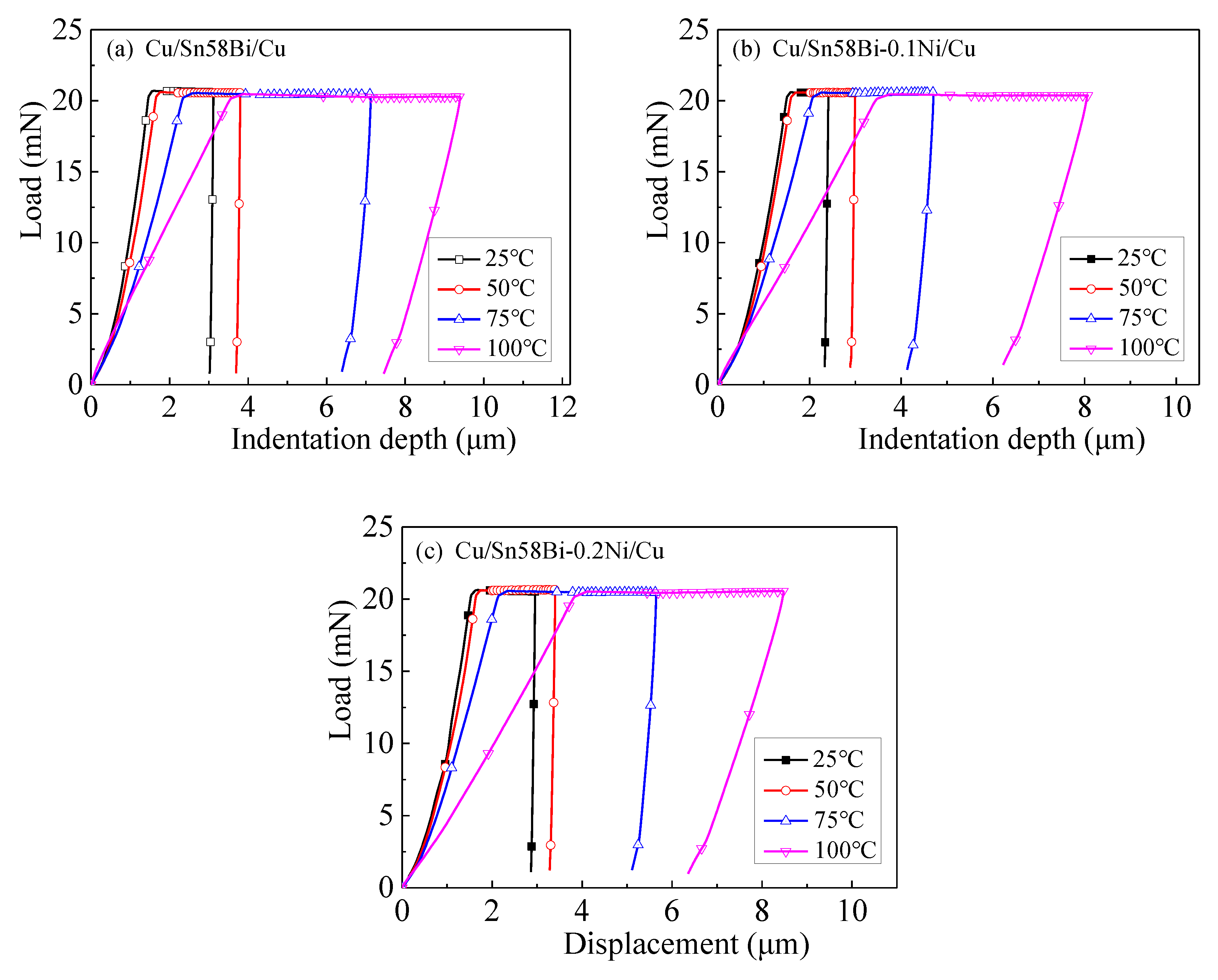
3.1. Indentation Load–Depth Curves versus Different Temperatures
3.2. Creep Displacement with Different Temperatures
3.3. Influence of Temperature on Indentation Morphology
3.4. Indentation Hardness at Different Temperatures
4. Conclusions
- (1)
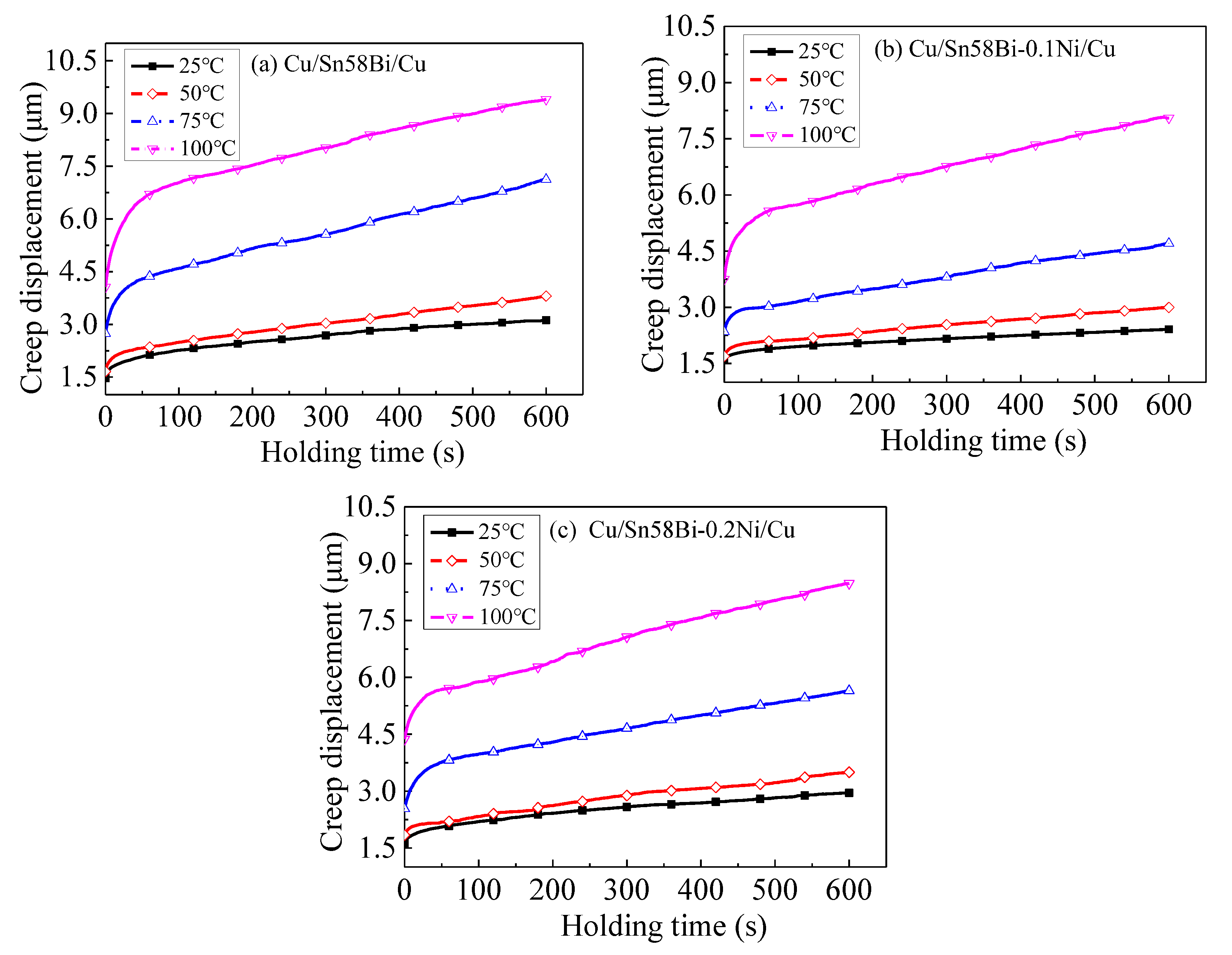
- Under the same experimental conditions, the initial indentation depth and creep displacement of Cu/Sn58Bi/Cu micro solder joints can be reduced by adding a small amount of Ni elements. The creep displacement values of Cu/Sn58Bi/Cu, Cu/Sn58Bi-0.1Ni/Cu, and Cu/Sn58Bi-0.2Ni/Cu micro solder joints at 75 °C were 4.39 ± 0.30 μm, 2.36 ± 0.24 μm and 3.11 ± 0.26 μm, respectively. Among the three types of micro solder joints, Cu/Sn58Bi-0.1Ni/Cu exhibited the best creep resistance at high temperatures.
- (2)
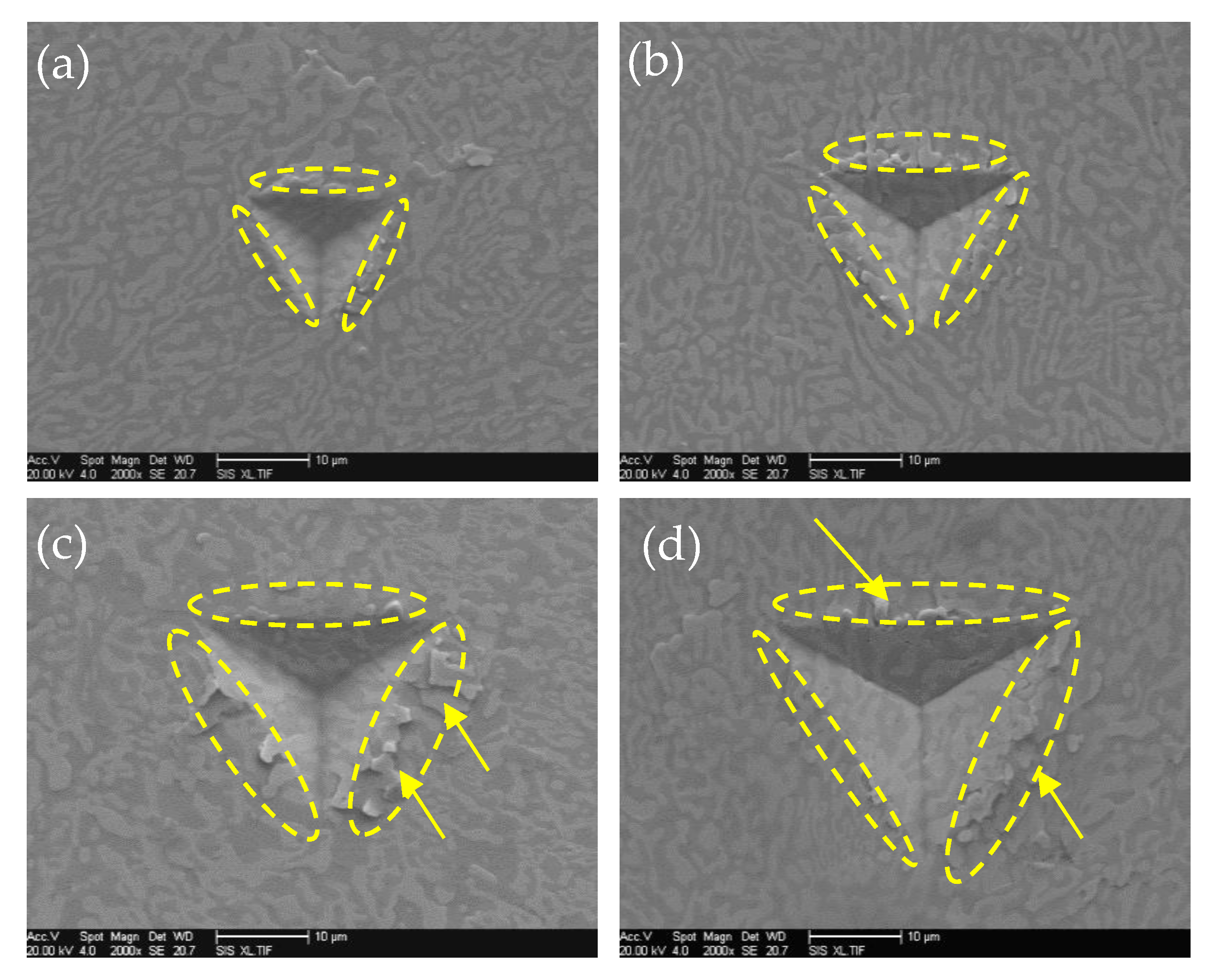
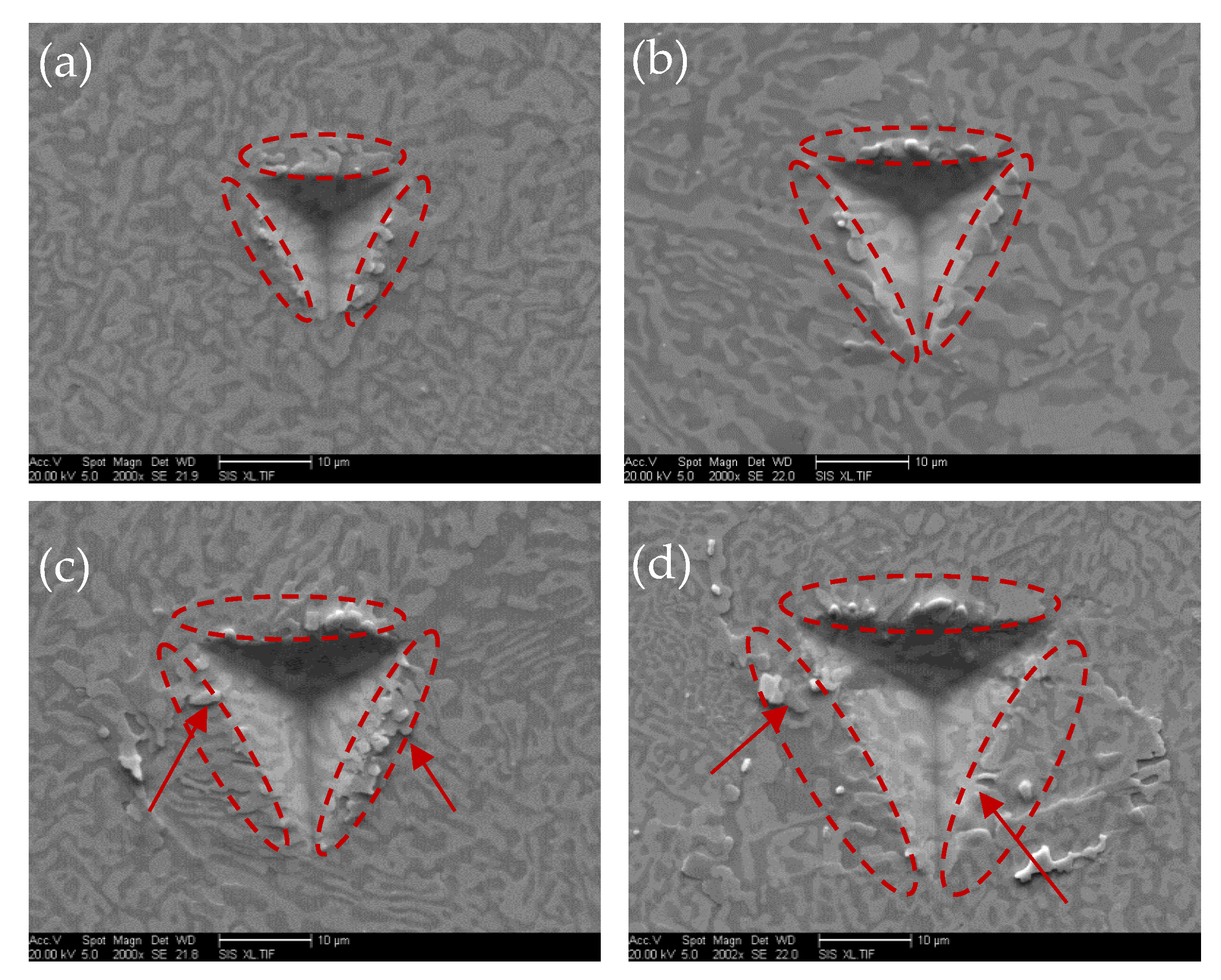
- According to the observation of the indentation morphology at different temperatures, it was found that there was accumulation around the indentation, especially at 75 °C and 100 °C. Compared with Cu/Sn58Bi/Cu micro solder joints, Cu/Sn58Bi-0.1Ni/Cu and Cu/Sn58Bi-0.2Ni/Cu had smaller indentation areas and less accumulation around the indentation. Ni doping can reduce the indentation area and accumulation phenomenon around the indentation.
- (3)
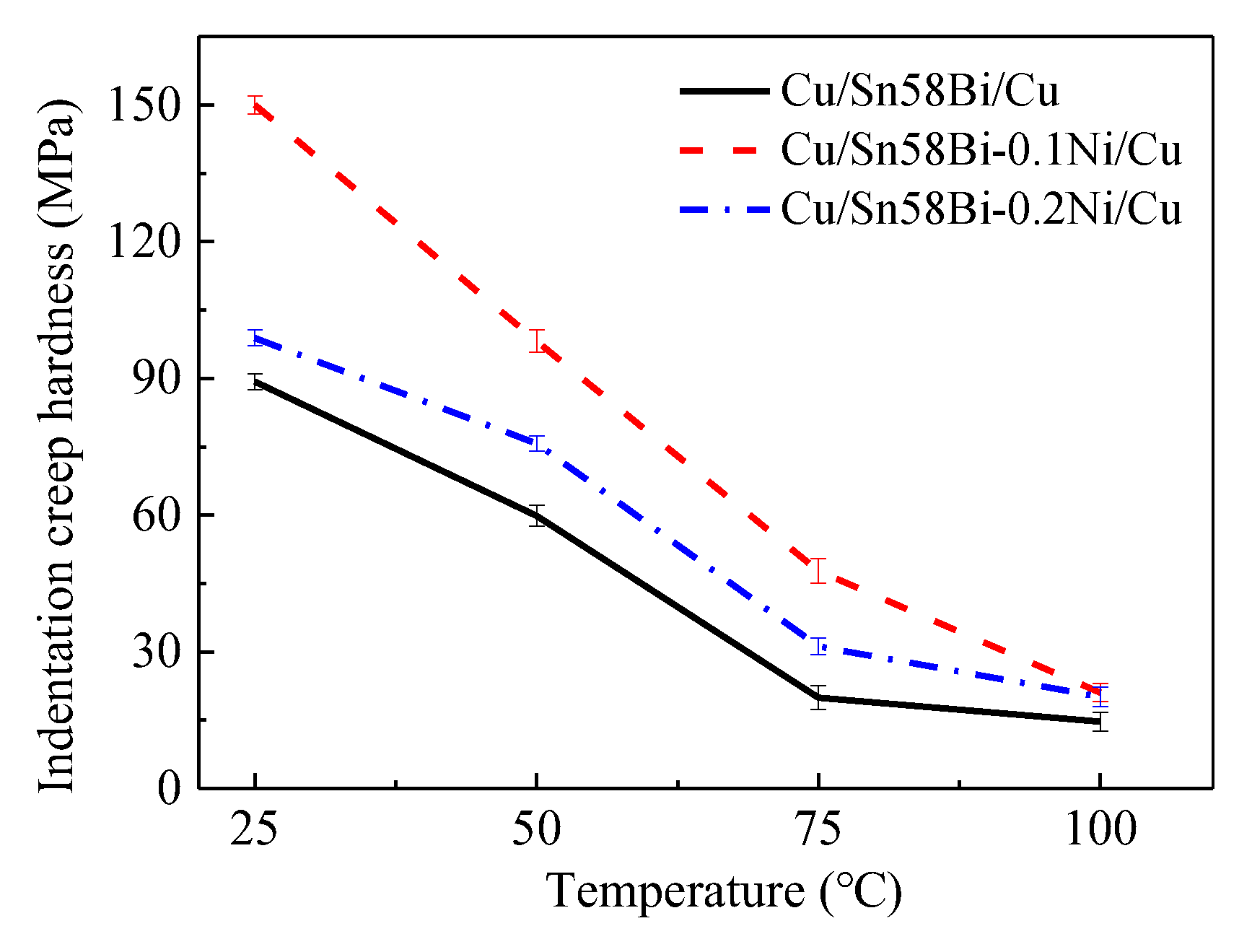
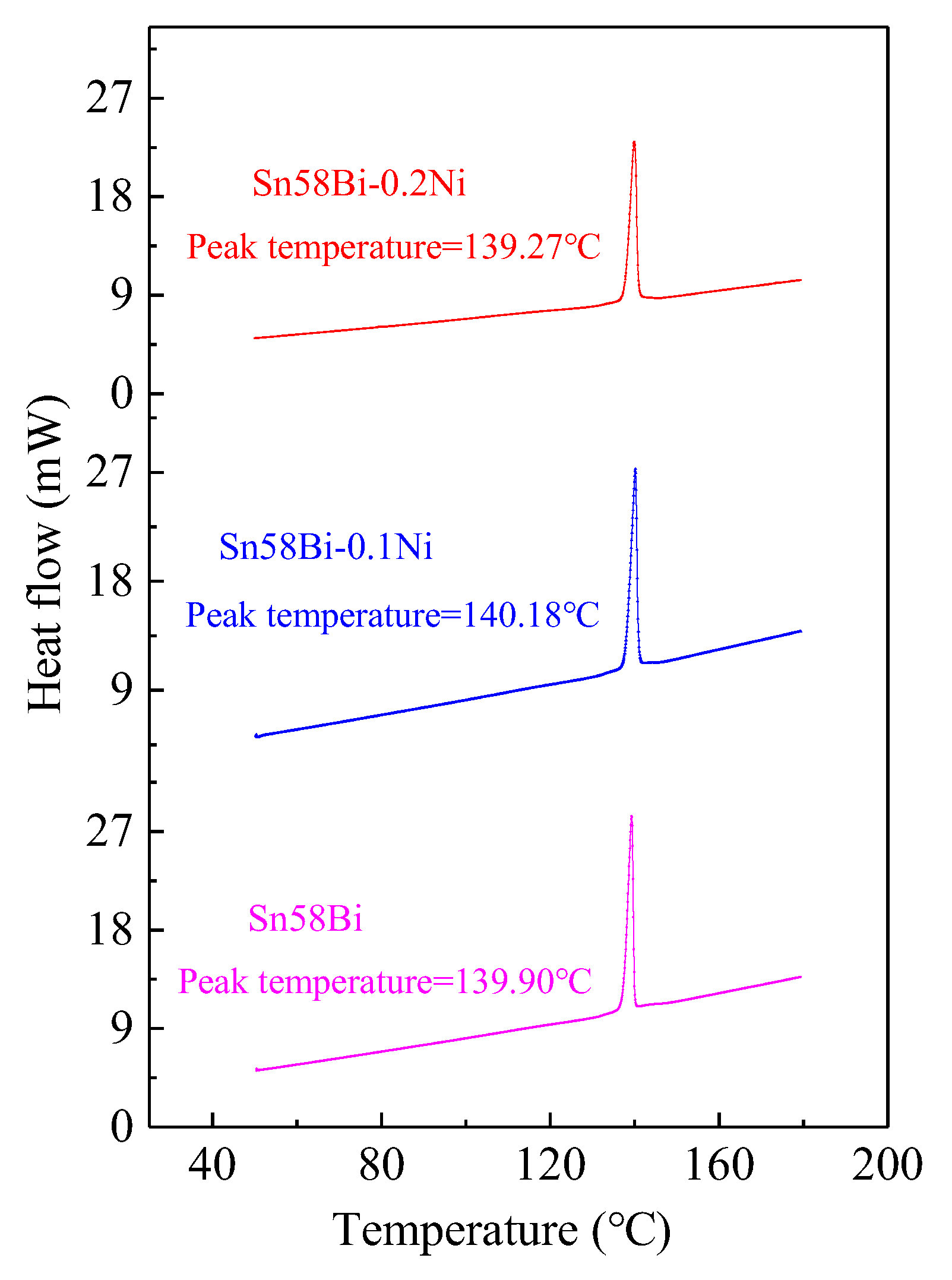
- The indentation hardness values of micro solder joints of Cu/Sn58Bi/Cu, Cu/Sn58Bi-0.1Ni/Cu, and Cu/Sn58Bi-0.2Ni/Cu at 100 °C were 14.67 ± 2.00 MPa, 21.05 ± 2.00 MPa, and 20.13 ± 2.10 MPa, respectively. Due to the melting points of the three types of solder alloys, which were 139.90 °C, 140.18 °C, and 139.27 °C, respectively, the solder softened during indentation testing at 100 °C, resulting in a sharp decrease in creep hardness.
Author Contributions
Funding
Institutional Review Board Statement
Informed Consent Statement
Data Availability Statement
Conflicts of Interest
References
- Tian, Y.N.; Jian, X.D.; Zhao, M.R.; Liu, J.H.; Dai, X.J.; Zhou, B.; Yang, X.F. Effect of thermal aging on the reliability of interconnected nano-silver solder joints. Crystals 2023, 13, 1630. [Google Scholar] [CrossRef]
- Song, Q.Q.; Yang, W.C.; Li, Y.T.; Mao, J.; Qin, W.O.; Zhan, Y.Z. Interfacial reaction and mechanical properties of Sn58Bi-XCr solder joints under isothermal aging conditions. Vacuum 2021, 194, 110559. [Google Scholar] [CrossRef]
- Gao, Y.; Zhang, K.; Zhang, C.; Wang, Y.; Chen, W. Microstructure and properties of electromigration of Sn58Bi/Cu solder joints with different joule thermal properties. Metals 2023, 13, 1475. [Google Scholar] [CrossRef]
- Dušek, K.; Buek, D.; Vesel, P.; Anna, P.; Plaek, M.; Re, J.D. Understanding the effect of reflow profile on the metallurgical properties of tin-bismuth solders. Metals 2022, 12, 121. [Google Scholar] [CrossRef]
- Singh, A.; Durairaj, R. Study on hardness and shear strength with microstructure properties of Sn52Bi/Cu+1% Al2O3 nanoparticles. In Proceedings of the IOP Conference Series: Materials Science and Engineering, Chennai, India, 16–17 September 2020; Volume 834, pp. 1–5. [Google Scholar]
- Liu, Y.; Chang, J.; Zhou, M.; Xue, Y.; Sun, F. Microstructure and shear behavior of Sn58Bi/Cu solder joint enhanced by SnAgCuBiNi bump. Mod. Phys. Lett. B 2020, 34, 2050413. [Google Scholar] [CrossRef]
- Hirata, Y.; Yang, C.H.; Lin, S.; Nishikawa, H. Improvements in mechanical properties of Sn-Bi alloys with addition of Zn and In. Mat. Sci. Eng. A-Struct. 2021, 813, 141131. [Google Scholar] [CrossRef]
- Kang, H.; Rajendran, S.H.; Jung, J.P. Low melting temperature Sn-Bi solder: Effect of alloying and nanoparticle addition on the microstructural, thermal, interfacial bonding, and mechanical characteristics. Metals 2021, 11, 364. [Google Scholar] [CrossRef]
- Shen, Y.A.; Zhou, S.; Li, J.; Tu, K.N.; Nishikawa, H. Thermomigration induced microstructure and property changes in Sn-58Bi solders. Mater. Des. 2019, 166, 107619. [Google Scholar] [CrossRef]
- Han, J.; Cao, H.; Meng, Z.; Jin, X.L.; Ma, L.M.; Guo, F.; An, T.; Wang, T. Study on electromigration mechanism of lead-free Sn3.5Ag0.5Bi8.0In solder joints. J. Electron. Mater. 2023, 52, 1216–1232. [Google Scholar] [CrossRef]
- Wang, X.; Zhang, L.; Chen, C.; Lu, X. Effect of AlN on the microstructure evolution of Cu/Sn58Bi/Cu solder joints for 3D packaging at different bonding times. J. Mater. Res. Technol. 2023, 25, 4488–4496. [Google Scholar] [CrossRef]
- Yang, L.; Ma, S.; Mu, G. Improvements of microstructure and hardness of lead-free solders doped with Mo nanoparticles. Mater. Lett. 2021, 304, 130654. [Google Scholar] [CrossRef]
- Singh, A.; Durairaj, R.; Kumar, K.G.; Kuan, S.H. Impact of 3% Molybdenum(Mo) nanoparticles on the interfacial and shear properties of lead-free Sn58Bi/Cu solder joint. In Proceedings of the IOP Conference Series: Materials Science and Engineering, Chandigarh, India, 4–5 March 2022; p. 012029. [Google Scholar]
- Li, Y.; Yu, S.; Li, L.; Song, S.; Qin, W.; Qi, D.; Yang, W.; Zhan, Y. A review on the development of adding grapheneto Sn-based lead-free solder. Metals 2023, 13, 1209. [Google Scholar] [CrossRef]
- Huang, X.; Zhang, L.; Chen, C.; Lu, X.; Wang, X. Comprehensive analysis of Sn58Bi/Cu solder joints reinforced with Mg particles: Wettability, thermal, mechanics, and microstructural characterization. J. Mater. Res. Technol. 2023, 27, 2641–2655. [Google Scholar] [CrossRef]
- Jeong, G.; Yu, D.Y.; Baek, S.; Bang, J.H.; Ko, Y.H. Interfacial reactions and mechanical properties of Sn-58Bi solder joints with Ag nanoparticles prepared using ultra-fast laser bonding. Materials 2021, 14, 335. [Google Scholar] [CrossRef]
- Yang, F.; Zhang, L.; Liu, Z.Q.; Zhong, S.; Ma, J.; Bao, L. Effects of CuZnAl particles on properties and microstructure of Sn-58Bi solder. Materials 2017, 10, 558. [Google Scholar] [CrossRef] [PubMed]
- Qin, W.; Yang, W.; Zhang, L.; Qi, D.; Song, Q.; Zhan, Y. Effect of Ni-modified reduced graphene oxide on the mechanical properties of Sn-58Bi solder joints. Vacuum 2023, 211, 111943. [Google Scholar] [CrossRef]
- Nogita, K.; Nishimura, T. Nickel-stabilized hexagonal (Cu, Ni)6Sn5 in Sn-Cu-Ni lead free solder alloys. Scripta Mater. 2008, 59, 191–194. [Google Scholar] [CrossRef]
- Nogita, K.; Mcdonald, S.D.; Tsukamoto, H.; Read, J.; Nishimura, T. Inhibiting cracking of interfacial Cu6Sn5 by Ni additions to Sn-based lead-free solders. Trans. Jpn. Inst. Electron. Packag. 2009, 2, 46–54. [Google Scholar] [CrossRef]
- Kanlayasiri, K.; Ariga, T. Physical properties of Sn58Bi-xNi lead-free solder and its interfacial reaction with copper substrate. Mater. Des. 2015, 86, 371–378. [Google Scholar] [CrossRef]
- Yang, L.Z.; Zhou, W.; Ma, Y.; Li, X.Z.; Liang, Y.H.; Cui, W.Q.; Wu, P. Effects of Ni addition on mechanical properties of Sn58Bi solder alloy during solid-state aging. Mat. Sci. Eng. A 2016, 667, 368–375. [Google Scholar] [CrossRef]
- Fleshman, C.; Duh, J.G. The variation of microstructure and the improvement of shear strength in SAC1205-xNi/OSP Cu solder joints before and after aging. J. Electron. Mater. 2020, 49, 196–201. [Google Scholar] [CrossRef]
- Cao, C.C.; Zhang, K.K.; Shi, B.J.; Wang, H.G.; Zhao, D.; Sun, M.M.; Zhang, C. The interface microstructure and shear strength of Sn2.5Ag0.7Cu0.1RExNi/Cu solder joints under yhermal-cycle loading. Metals 2019, 9, 518. [Google Scholar] [CrossRef]
- Yang, L.Z.; Zhou, W.; Li, X.Z.; Ma, Y.; Liang, Y.H.; Cui, W.Q.; Wu, P. Effect of Ni and Ni-coated Carbon Nanotubes on the interfacial reaction and growth behavior of Sn58Bi/Cu intermetallic compound layers. J. Mater. Sci. Mater. Electron. 2016, 27, 12264–12270. [Google Scholar] [CrossRef]
- Wang, H.Z.; Hu, X.W.; Jiang, X.G. Effects of Ni modified MWCNTs on the microstructural evolution and shear strength of Sn-3.0Ag-0.5Cu composite solder joints. Mater. Charact. 2020, 163, 110287. [Google Scholar] [CrossRef]
- Zhang, H.W.; Liu, Y.; Wang, J.; Sun, F.L. Failure study of solder joints subjected to random vibration loading at different temperatures. J. Mater. Sci.-Mater. Electron. 2015, 26, 2374–2379. [Google Scholar] [CrossRef]
- Khodabakhshi, F.; Zareghomsheh, M.; Khatibi, G. Nanoindentation creep properties of lead-free nanocomposite solders reinforced by modified carbon nanotubes. Mat. Sci. Eng. A 2020, 797, 140203. [Google Scholar] [CrossRef]
- Cordova, M.E.; Shen, Y.L. Indentation versus uniaxial power-law creep: A numerical assessment. J. Mater. Sci. 2015, 50, 1394–1400. [Google Scholar] [CrossRef]
- Qun, L.I.; Huang, J.H.; Zhang, H.; Zhao, X.K.; Qi, L.H. Influence of Al on microstructure and mechanical properties of the Sn-58Bi lead-free solder. Electron. Process Technol. 2008, 29, 3471–3474. [Google Scholar]
- Yang, L.Z.; Zhou, W.; Liang, Y.H.; Cui, W.Q.; Wu, P. Improved microstructure and mechanical properties for Sn58Bi solder alloy by addition of Ni-coated carbon nanotubes. Mater. Sci. Eng. A 2015, 642, 7–15. [Google Scholar] [CrossRef]
- Fan, J.J.; Jiang, D.W.; Zhang, H.; Hu, D.; Liu, X.; Fan, X.J.; Zhang, G.Q. High-temperature nanoindentation characterization of sintered nano-copper particles used in high power electronics packaging. Results Phys. 2022, 33, 105168. [Google Scholar] [CrossRef]
- Thornby, J.; Harris, A.; Bird, A.; Beake, B.; Haghshenas, M. Micromechanics and Indentation Creep of Magnesium Carbon Nanotube Nanocomposites: 298 K–573 K. Mater. Sci. Eng. A 2021, 801, 140418. [Google Scholar] [CrossRef]
- El-Daly, A.A.; Hammad, A.E.; Fawzy, A.; Nasrallh, D.A. Microstructure, mechanical properties, and deformation behavior of Sn-1.0Ag-0.5Cu solder after Ni and Sb additions. Mater. Des. 2013, 43, 40–49. [Google Scholar] [CrossRef]
- Che, F.X.; Zhu, W.H.; Poh, E.S.W.; Zhang, X.R.; Zhang, X.W.; Chai, T.C.; Gao, S. Creep properties of Sn-1.0Ag-0.5Cu lead-free solder with Ni addition. J. Electron. Mater. 2011, 40, 344–354. [Google Scholar] [CrossRef]
- Silva, B.L.; Cheung, N.; Garcia, A.; Spinelli, J.E. Sn-0.7wt%Cu-(xNi) alloys: Microstructure-mechanical properties. correlations with solder/substrate interfacial heat transfer coefficient. J. Alloys Compd. 2015, 632, 274–285. [Google Scholar] [CrossRef]
- Han, Y.D.; Gao, Y.; Zhang, S.T.; Jing, H.Y.; Xu, L.Y. Study of mechanical properties of Ag nanoparticle-modified graphene/Sn-Ag-Cu solders by nanoindentation. Mater. Sci. Eng. 2019, 761, 138051.1–138051.13. [Google Scholar] [CrossRef]
- Fischer-Cripps, A.C. Nanoindentation Testing; Springer: New York, NY, USA, 2011; pp. 89–90. [Google Scholar]
- Li, W.B.; Warren, R. A model for nano-indentation creep. Acta Metall. Mater. 1993, 41, 3065–3069. [Google Scholar] [CrossRef]
- Shen, L.; Tan, Z.Y.; Chen, Z. Nanoindentation study on the creep resistance of SnBi solder alloy with reactive nano-metallic fillers. Mater. Sci. Eng. A 2013, 561, 232–238. [Google Scholar] [CrossRef]
- Sun, Y.; Liang, J.; Xu, Z.H.; Wang, G.F.; Li, X.D. Nanoindentation for measuring individual phase mechanical properties of lead free solder alloy. J. Mater. Sci.-Mater. Electron. 2008, 19, 514–521. [Google Scholar] [CrossRef]
- Geng, D.C.; Yu, H.; Okuno, Y.; Kondo, S.; Kasada, R. Practical method to determine the effective zero-point of indentation depth for continuous stiffness measurement nanoindentation test with Berkovich tip. Sci. Rep. 2022, 12, 6391. [Google Scholar] [CrossRef]


Disclaimer/Publisher’s Note: The statements, opinions and data contained in all publications are solely those of the individual author(s) and contributor(s) and not of MDPI and/or the editor(s). MDPI and/or the editor(s) disclaim responsibility for any injury to people or property resulting from any ideas, methods, instructions or products referred to in the content. |
© 2024 by the authors. Licensee MDPI, Basel, Switzerland. This article is an open access article distributed under the terms and conditions of the Creative Commons Attribution (CC BY) license (https://creativecommons.org/licenses/by/4.0/).
Share and Cite
Kong, X.; Zhai, J.; Ma, R.; Sun, F.; Li, X. Mechanical Response of Cu/Sn58Bi-xNi/Cu Micro Solder Joint with High Temperatures. Crystals 2024, 14, 269. https://doi.org/10.3390/cryst14030269
Kong X, Zhai J, Ma R, Sun F, Li X. Mechanical Response of Cu/Sn58Bi-xNi/Cu Micro Solder Joint with High Temperatures. Crystals. 2024; 14(3):269. https://doi.org/10.3390/cryst14030269
Chicago/Turabian StyleKong, Xiangxia, Junjun Zhai, Ruipeng Ma, Fenglian Sun, and Xuemei Li. 2024. "Mechanical Response of Cu/Sn58Bi-xNi/Cu Micro Solder Joint with High Temperatures" Crystals 14, no. 3: 269. https://doi.org/10.3390/cryst14030269