Abstract
The prototype misfit layer compound (SnS)1.17NbS2 consists alternatingly of a metallic triatomic NbS2 layer, in which Nb atoms are sandwiched by S atoms, and an insulating SnS double layer featuring a NaCl-type structure. Here we investigate the effect of lattice misfit on the stability and chemical bonding in the misfit layer compound using a first-principles density functional theory approach. The calculations show that for the (SnS)1+xNbS2 approximants, the most stable one has x = 0.167, close to the experimental observations. Charge analysis finds a moderate charge transfer from SnS to NbS2. Sn or S vacancies in the SnS part affect the electronic properties and interlayer interactions. The obtained information here helps in understanding the mechanism of formation and stability of misfit layer compounds and ferecrystals and further contributes to the design of novel multilayer compounds and emerging van der Waals heterostructures.
1. Introduction
Since their discovery in the late 1980s, misfit layer compounds have been a topic of intensive investigation [1,2]. These compounds have the chemical formula (MX)1+xTX2 (M = Sn, Pb, Bi, Sb, rare earth elements; X = S, Se, Te; T = Ti, V, Cr, Nb, and Ta), with planar intergrowth structures [1,2,3,4]. Both MX and TX2 parts have subnano-sized thicknesses. The MX part typically consists of a bi-atomic layer of a distorted rock-salt-type constituent, and the TX2 part consists of a triatomic layer with a transition metal atom (T) sandwiched by two X atoms. The intra-interactions in both MX and TX2 parts are strong, whereas the interlayer interactions between MX and TX2 are weak, being van der Waals-type. Structurally the two parts are incommensurate in at least one orientation. Crystallographically these compounds lack three-dimensional periodicity. Misfit layer compounds exhibit unusual physical properties [1,4,5,6,7,8] and potential applications, particularly as two-dimensional electronic devices [4,5,6,9,10,11]. Moreover, lattice misfits provide a platform on which to explore the energetics and local bonding constraints of heterostructures and to engineer novel quantum fabrics and electronic properties [5,6,7].
Both experimental and theoretical efforts have been made to understand the stability of and chemical bonding in misfit layer compounds. Experimentalists have focused on synthesis for new forms, e.g., nanotubes [1,4,5,9,10,11,12,13,14], structural determination using super-space group theory [1,15,16,17], measurements of physical properties including electrical and thermal transport and electronic and magnetic properties [4,5,6,8,18,19,20], and spectroscopic characteristics [4,21,22,23,24,25,26,27]. The experiments have provided an improved understanding of the electronic properties and chemical bonding in these systems. Recent progress includes new synthesis approaches and produces new members, including ferecrystals, which have thicker MX or TX2 layers [28,29].
Theoretical efforts have been made to understand the chemical bonding in misfit layer compounds [22,25,29,30,31,32,33,34,35,36,37]. Bond analysis has been applied to investigate the interlayer interactions, including charge transfer [22,30,31]. First-principles band structure calculations have been applied to various misfit layer compounds to gain insight into the interlayer interactions [22,25,32,33,34,35,36,37]. Nevertheless, the dependence of lattice misfit on stability and chemical bonding is still largely unknown.
(SnS)1.17NbS2 has been regarded as a prototype of misfit layer compounds [1,4,5,38]. The structure of this compound was determined using the single-crystal X-ray diffraction approach [38,39]. It consists alternatingly of a metallic NbS2 triatomic layer, with Nb atoms sandwiched by S atoms, and an insulating SnS bi-atomic layer featuring a distorted NaCl-type atomic arrangement. Both NbS2 and SnS subsystems have C-centered orthorhombic unit cells, which do not match along the in-plane <100> orientation. Electrical transport property measurements revealed that this misfit compound is p-type metallic with about 0.87e/Nb holes according to the Hall effect measurements [38]. Photoemission spectroscopy revealed the near-complete occupation of the Nb 4d states, indicating charge transfer from the (SnS) part to the (NbS2) part [22,23,40]. (SnS)1.17NbS2 was the first misfit layer compound whose band structure was investigated by first-principles density functional theory within the local-density approximation (LDA) for an approximant (SnS)1.20NbS2 [22]. Charge transfer from the SnS layer to the NbS2 layer was revealed. However, in the early calculation, van der Waals forces and the effect of the misfit parameter x in the formula (SnS)1+xNbS2 were not included. Recently, Gotoh [31] determined the atomic modulation in the two-dimensional (2D) misfit layer (SnS)1.17NbS2 by means of accurate modeling of incommensurate composite crystal structure. The study suggested a sulfur vacancy in the SnS part. Based on first-principles band structure calculations, the La vacancy in the LaS part was proposed in the misfit layer compound (LaS)1.20CrS2 [36,37]. Kabliman et al. performed an ab initio investigation on the stability of (PbS)1.14TaS2 using different ratios of PbS and TaS2 and obtained the composition range of high stability with respect to the parental binary compounds [33].
Recent progress in computational material sciences has enabled the study of larger systems with high reliability and accuracy. The stability of the misfit layer compound (SnS)1.17NbS2 is investigated here using the approximants (SnS)1+xNbS2 with x = 0.200, 0.167, and 0.143, using first-principles density functional theory with van der Waals corrections created by Klimes et al. [41,42]. Furthermore, the effects of Sn or S vacancies in the SnS part on the electronic properties and interlayer bonding are examined. The information obtained here is not only helpful for gaining insight into the stability, chemical compositions, crystal structure, and chemical bonding in the misfit layer compound (SnS)1.17NbS2 and other misfit layer compounds [1,2,3,4,22], but also relevant to ferecrystals and their modification via doping [10,24,28], and even other unusual materials, such as FeCl3/graphene with misfit characteristics [43].
2. Details of Computational Methods
2.1. Supercells for Misfit Layer Compound (SnS)1+xNbS2 Approximants
A plane wave approach was employed in the present study, which utilizes the periodic boundary conditions. Thus, supercells were built [44]. According to the experimental observations [1,4,38,39] and previous work [22], the designed supercells had different misfit parameters and symmetry. The created configurations involved shifting the SnS part along the misfit direction to contain different types of interlayer bonding. Sn/S vacancies were also included within (SnS)1.167NbS2. In the formula (SnS)1+xNbS2, seven input configurations were produced: case (a) x = 0.200, based on the previous work [22]; case (b) x = 0.167 and case (c) x = 0.167, with atoms in the SnS part shifted along the misfit orientation; and case (d) x = 0.143. Configurations of S vacancy (i) with symmetry (case (e)) and (ii) without symmetry (case (f)) were included, both with x = 0.167. Case (g) has the configuration with x = 0.167 and Sn vacancies.
The formation energy of the misfit layer compound (SnS)1+xNbS2 with respect to the binaries, SnS and NbS2, is defined as
ΔE((SnS)1+xNbS2) = E((SnS)1+xNbS2) − [(1 + x) E(SnS) + E(NbS2)]
Here, E((SnS)1+xNbS2), E(SnS), and E(NbS2) represent the calculated total-valence-electron energy of (SnS)1+xNbS2 and the parental binaries α-SnS and 3R-NbS2, respectively. The unit of formation energy, ΔE, is eV per NbS2. A negative sign of ΔE means an exothermic relation from the binaries to the ternary compound. At 0 K and 0 Pa, the formation energy is equal to the formation enthalpy, ΔE = ΔH if the zero-point vibration is ignored.
2.2. First-Principles Code and Settings
The first-principles code VASP [44] used in the present study employs the projector augmented wave method [45] within the generalized gradient approximation formulated by Perdew, Burke, and Ernzerhof (GGA-PBE) [46]. The van der Waals density functional by Klimes, et al. (vdW-DF2) [41,42] was utilized since it works well for various systems [41,47]. The atomic electronic configurations are Nb ({[Ar] 3d10 4s2} 4p6 4d4 5s2 5p1), S ([Ne] 3s2 3p4), and Sn ({[Kr] 4d10} 5s2 5p2). The symbol {} represents frozen core electrons, and the rest are the valence electrons, which include the semicore Nb 4p6 electrons.
High cut-off energies of 400.0 eV for the wave functions and 550.0 eV for the augmentation functions were used. Those values are notably higher than the corresponding default values (EMAX/EAUG = 293.2/455.7 eV for Nb, 258.7/335.1 eV for Sn, and 103.2/263.6 eV for Sn, respectively). Dense k-meshes were used for sampling the electronic wave functions, e.g., a 24 × 24 × 8 (449 k-points) k-mesh and an 8 × 24 × 24 (845 k-points) k-mesh in the Brillouin zones (BZ) of 3R-NbS2 and α-SnS, respectively, based on the Monkhorst-Pack scheme [48]. A 4 × 10 × 6 k-mesh was used for cases (a) and (d), and a 2 × 10 × 6 k-mesh for the other approximants. Test calculations using different cut-off energies and k-meshes demonstrated that the settings are reliable and produce results with deviations within 1 meV/atom.
3. Results
3.1. The Parental SnS and NbS2 Phases
The parental binary compounds, SnS and NbS2, are first investigated using the code and settings in Section 2. There are two phases of SnS reported in the literature [22,49,50,51]. A novel phase featuring a NaCl-type structure is also included. Experiments revealed that both 2H- and 3R-NbS2 exist at ambient conditions [52,53]. There are two types of atomic arrangement for the 2H phase. Table 1 shows the obtained results.

Table 1.
Calculated results (Lattice parameters, volumes, and band gaps) for the binary compounds, (α- and β-)SnS and (2H-, 3R-)NbS2, using the DFT-GGA method with van der Waals interaction corrections.
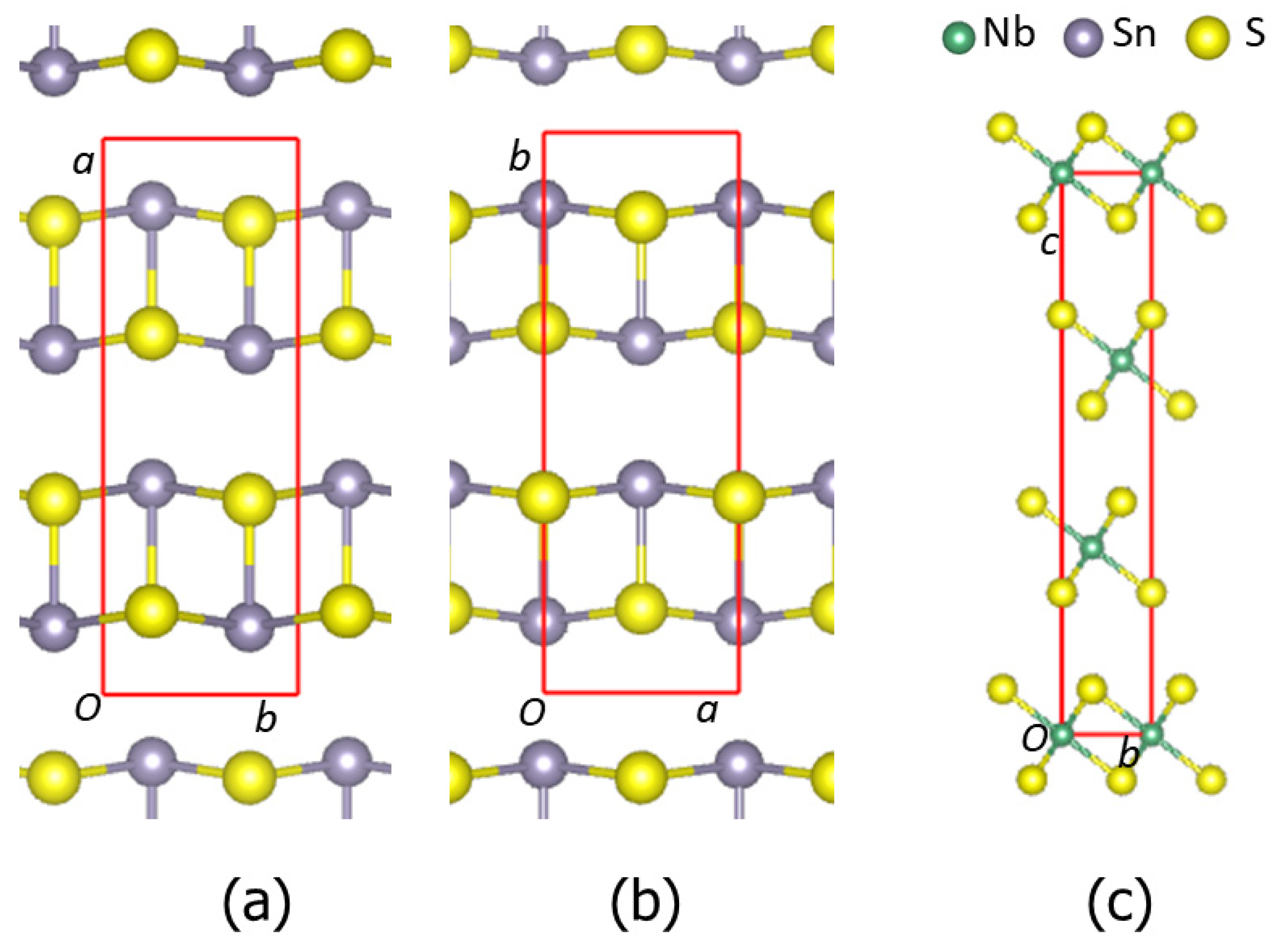
The calculations show that α-SnS is more stable than β-phase, while the phase featuring a NaCl-type structure is the least stable. The results agree with the experimental observation [49,50]. 3R-NbS2, whose structure is schematically shown in Figure 1c, is more stable than the 2H-phases (Table 1), in agreement with the experiments [52,53]. Table 1 also shows that the calculated lattice parameters of the SnS and NbS2 phases are close to their corresponding experimental values, indicating the applicability of the DFT-GGA approaches with van der Waals corrections [41,42,54] and the settings. Structurally, the α- and β-SnS phases are very similar: both are composed of zigzagged bi-atomic SnS layers along the α-SnS[1 0 0] and β-SnS[0 1 0] axis, as shown in Figure 1a and Figure 1b, respectively. The notable difference is the interlayer bonds. In α-SnS, there is weak interlayer bonding with an Sn-S bond length of 3.43 Å, whereas there is no direct bonding in β-SnS. The calculated densities of states for α- and β-SnS and 3R-NbS2 are shown in Figure 2.
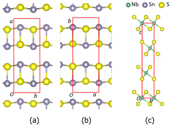
Figure 1.
Schematic structures of orthorhombic α-SnS along the [0 0 1] orientation (a), β-SnS along the [0 0 1] orientation (b), and 3R-NbS2 along the [1 0 0 0] orientation (c). Sn-S and Nb-S bonds within 3.0 Å are included. The small green spheres represent Nb, the large dark spheres represent Sn, and the golden spheres represent S.

Figure 2.
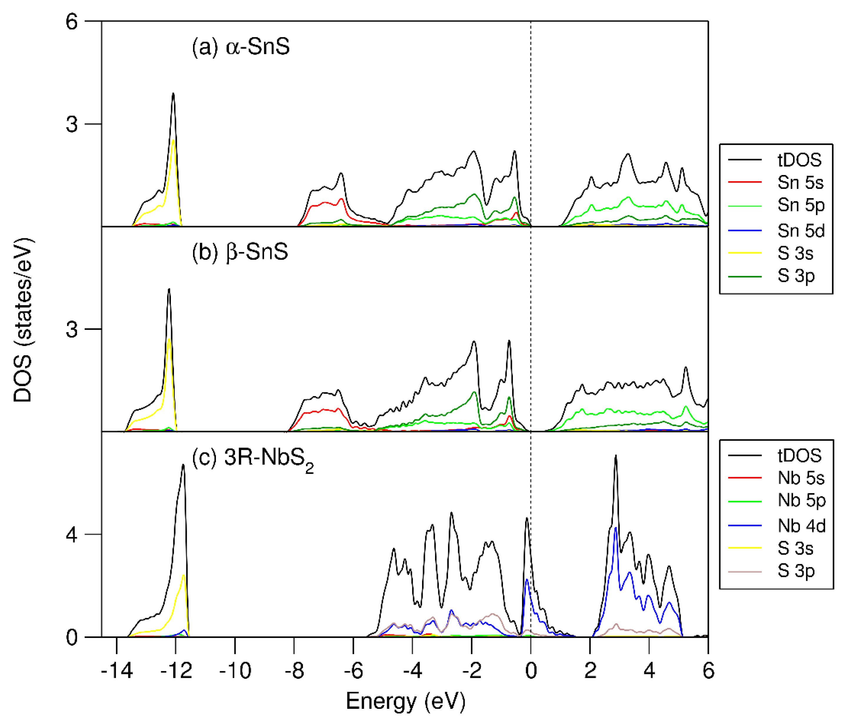
Calculated partial and total densities of states (PDOS and TDOS) for the reference binary compounds: (a) α-SnS, (b) β-SnS, and (c) 3R-NbS2. The perpendicular dotted line represents the Fermi level (zero eV).
The calculations show that the DOS curves of the SnS phases have similar frames, being composed of three parts. The lower part at −14.0 eV to −12.0 eV from the Fermi level (zero eV) is dominated by S 3s states. The valence band starts from about −8.0 eV and extends to the Fermi level. This part is dominated by Sn 5s, 5p, and S 3p states. It is notable that the Sn 5s states have a high density at the lower energy part, from −8.0 eV to −6.0 eV and from −1.0 eV to the Fermi level. Such large splitting of the lone-pair electrons indicates strong interaction with the S 3p states. However, in the SnS phases, both Sn 5s bonding (the lower part) and antibonding (the upper part) orbitals are fully occupied, indicating no contribution to the chemical bonding in the SnS phases. The conduction bands are dominated by Sn 5p and S 3p states. The calculated band gap for α-SnS is smaller than the experimental value, which is not unusual for standard density functionals, even with the van der Waals corrections [41,42,54]. Table 1 and Figure 2 show that (i) α-SnS is more stable than β-SnS, and (ii) the calculated band gap for α-SnS is larger than that for β-SnS. Such differences from the previous first-principles calculations using the local-density functional (LDA) and spherical wave approach [22,51] correspond to the advantage of GGA over LDA [54].
The DOS curve of 3R-NbS2 consists of three parts: the S 3s band, the valence band, and the conduction band. The S 3s states form a peak from −13.6 eV to −11.5 eV below the Fermi level. The valence band is composed of two parts. The lower part of the conduction band starts from −5.5 eV and extends to −0.4 eV, dominated by Nb 4d and S 3p states. There is a valley at −0.4 eV. The upper part of the valence band, in the range from −0.4 to 1.6 eV, is dominated by Nb 4d states. The peak of the Nb 4d states is at −0.1 eV. The Fermi level dominated by Nb 4d states hybridized with some S 3p states. Figure 2c shows a fraction of unoccupied Nb 4d states. There is a gap between the valence band and the conduction band. The conduction band starts from 2.1 eV, consisting of Nb 4d and S 3p states. The electronic structure shows a strong covalent nature.
3.2. Stability and Crystal Structure of (SnS)1+xNbS2 Approximants
First-principles calculations were performed for the designed misfit systems as mentioned in Section 2. The obtained results, including lattice parameters and formation energies according to Equation (1), are shown in Table 2. The optimized structures are schematically shown in Figure 3. The atomic coordinates and chemical bonds of the selected systems are included in the Supplementary Materials (Table S2 for case (a), Table S3 for case (b), Table S4 for case (d), Table S5 for case (e), and Table S6 for case (f), respectively). The chemical bonding in the most stable (SnS)1.167NbS2 (case (b) in Table 2) is listed in Table 3.
Table 2.
Calculated lattice parameters and formation energies of the approximants of the (SnS)1+xNbS2 compound with respect to α-SnS and 3R-NbS2 from the GGA-vdW calculations (Equation (1)). The deviation of the lengths of the axis in parentheses is defined as Δ = (dcalc. − dexp)/dexp. × 100%. * Pseudo-orthorhombic unit cells. Z represents the number of chemical formulas in the cell. The formation energies, ΔE, are obtained according to Equation (1).
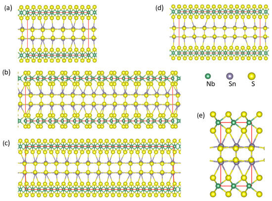
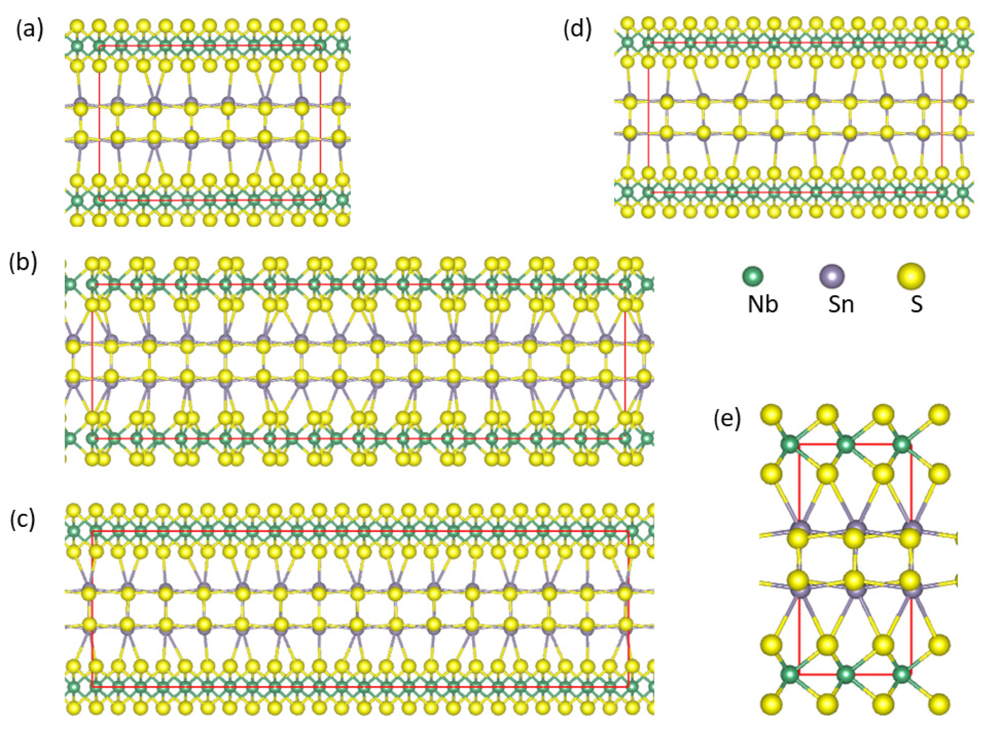
Figure 3.
Schematic structures of the misfit layer compound (SnS)1+xNbS2 with the [0 1 0] projections with the commensurate approximants, x = 0.200 (a), x = 0.143 (d), x = 0.167 (b,c) with SnS-shifts. The schematic structure of (SnS)1+xNbS2 with the [1 0 0] projection is shown in (e). The meaning of the spheres is as follows: The small green spheres represent Nb, the large dark spheres represent Sn, and the golden spheres represent S. Sn-S and Nb-S bonds with lengths less than 3.5 Å are shown.
Table 3.
The calculated values (chemical bonds, charges at atomic sites) for the (SnS)1.167NbS2 approximant, case (b).
Figure 3b,c show that the SnS shifts induce slight rearrangements of the S atoms in NbS2 (S(Nb), in short) and Nb atoms, and the calculated lattice parameters differ slightly from the pristine one as shown in Table 2. Table 2 also shows little energy difference between the two structural configurations. Structural analysis also found no significant differences in the interatomic distances. These results indicate the flexibility of such misfit structures.
The calculations revealed that all the structures (cases a–d) have negative formation energies with respect to the stable binary compounds, α-SnS and 3R-NbS2. The structures with x = 0.167 (cases (b) and (c) in Table 2) have the lowest energies. The energy difference between case (b) and case (c) is minor, indicating the flexibility of the misfit layer compound. This composition is close to the experimental value (x = 0.171). Therefore, the previous commensurate approximant with x = 1.20 deviates from the experimental observations.
As shown in Table 3, the Nb-S bonding in all the compositions and structures in the NbS2 part have the Nb-S bond lengths ranging from 2.47 to 2.50 Å, which are close to that of the bulk 3R-NbS2 (2.49 Å). In the SnS part, each Sn has five S neighbors with Sn-S bond lengths ranging from 2.64 Å to 3.0 Å, which are close to those in β-SnS (Table 1). Each Sn has generally one long interlayer Sn-S(Nb) bond with bond lengths of about 3.2 Å, which are in the range of van der Waals bonding.
3.3. Electronic Structure of (SnS)1.167NbS2
First-principles electronic band-structure calculations were performed for the most stable configuration. The obtained density of states (DOS) and band dispersion curves along the high symmetry lines are shown in Figure 4 and Figure 5, respectively.
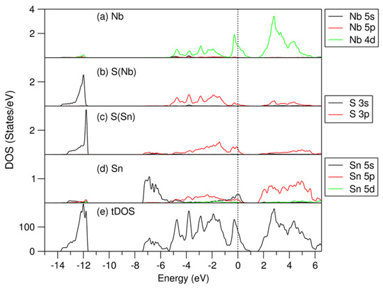
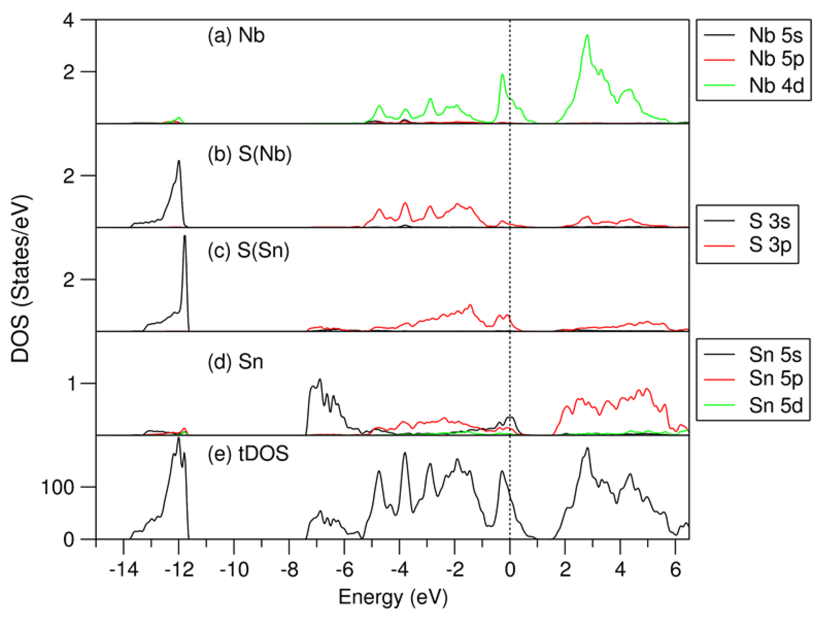
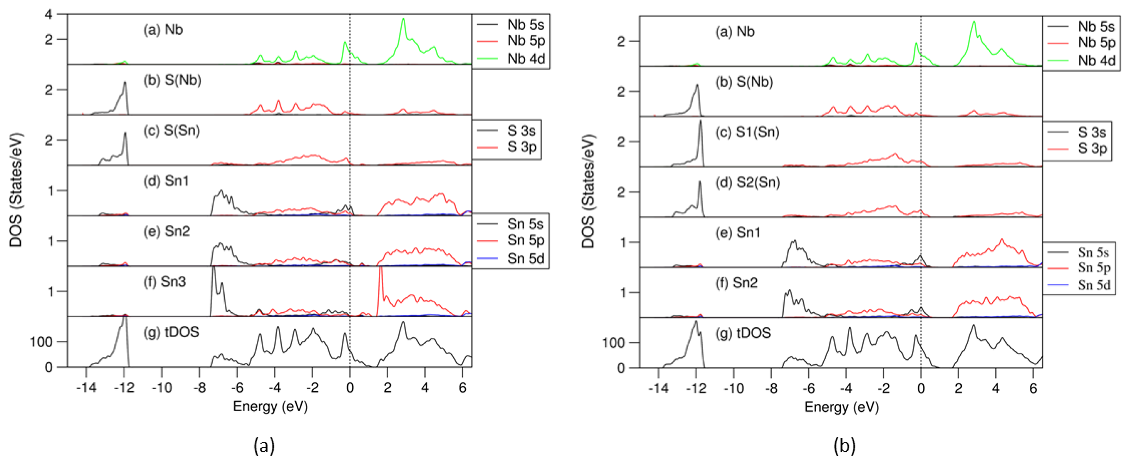
Figure 4.
Partial density of states for selected atoms: (a) for Nb, (b) for S(Nb), (c) for S(Sn), (d) for Sn, and total density of states (e) for the most stable (SnS)1.167NbS2 structure. The perpendicular dotted line represents the Fermi level at zero eV.
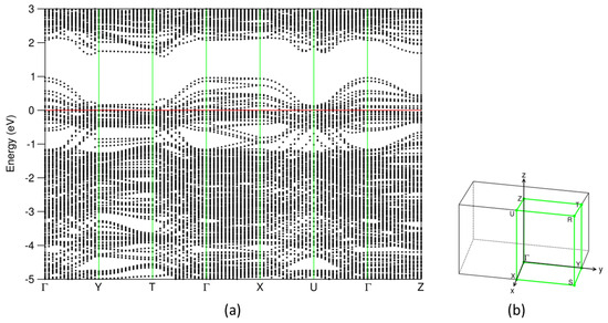
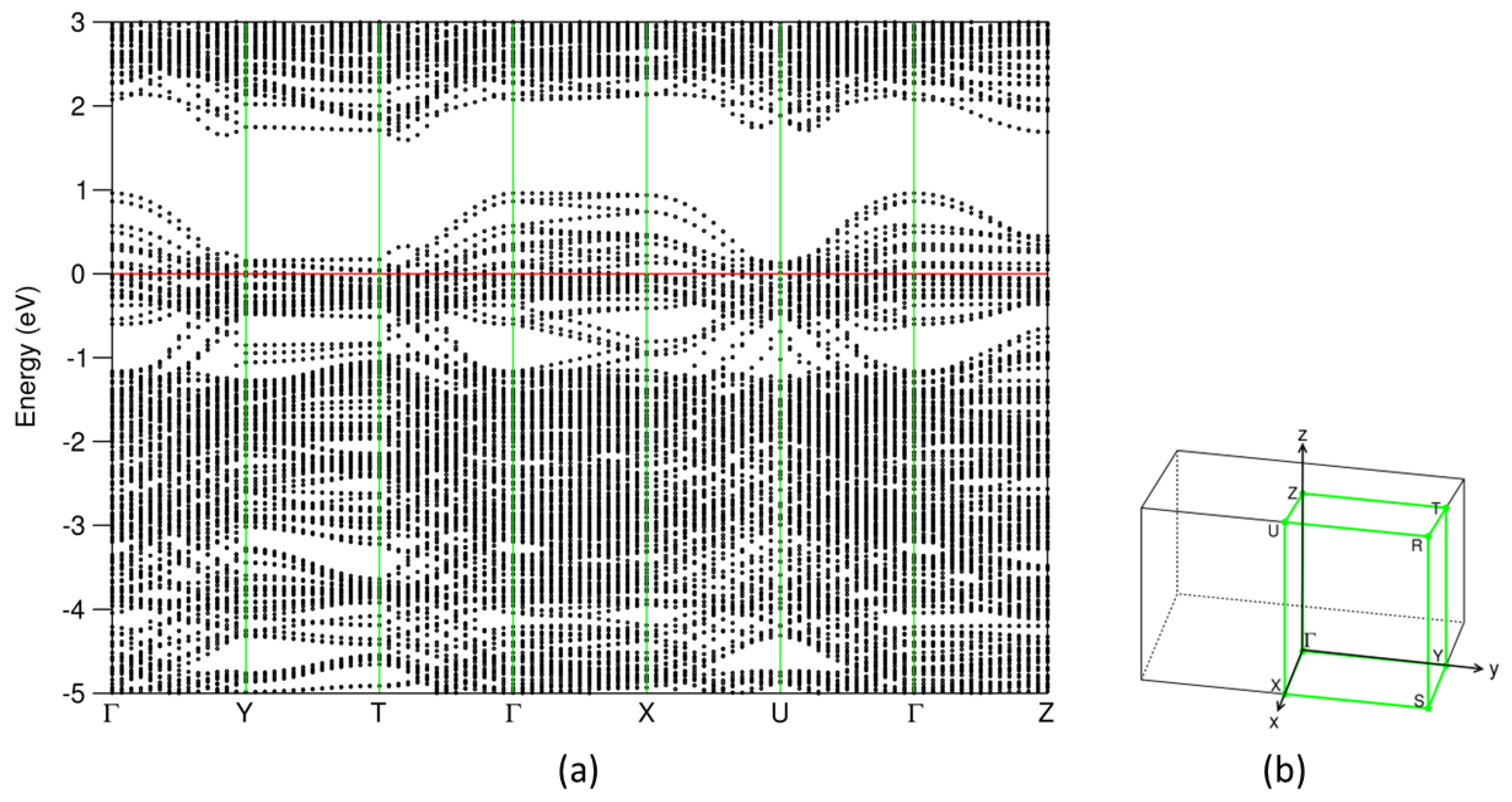
Figure 5.
(a) Dispersion curves along the high-symmetry lines around the Fermi level in (b) the Brillouin zone for the most stable (SnS)1.167NbS2 structure. The filled red horizontal line represents the Fermi level at zero eV.
As shown in Figure 4 and Figure 5, the electronic band structure of (SnS)1.167NbS2 consists of three separated parts, which is in line with the previous calculations for the (SnS)1.20NbS2 approximant using the DFT-LDA approximation [22]. Meanwhile, careful analysis revealed subtle differences.
The lowest part ranging from −13.8 eV to −11.6 eV consists of S 3s states. The S(Nb) 3s states in the NbS2 part are positioned lower in energy than those in the SnS part (S(Sn), in short). The peak of S(Nb) 3s is at −12.0 eV, which is about 0.2 eV lower in energy than that of S(Sn). This result is opposite to the DOS curves of the binary components, in which the S(Sn) 3s electrons have energies lower than that of S(Nb) (Figure 2). This relates to interlayer interaction and charge transfer in the misfit layer compound. There is an energy gap of about 4.2 eV, separating the S 3s states from the valence band.
The valence band starts at −7.4 eV and ends at 1.0 eV. The Sn 5s states dominate the lower part in the energy range from −7.4 eV to −5.5 eV. Interestingly, there are Sn 5s states around the Fermi level, and there are unoccupied Sn 5s states (Figure 4d), indicating that the inert Sn 5 s2 pair-electrons participate in the chemical bonding. This phenomenon agrees with the previous study on the transition metal dichalcogenides intercalated by post-transition metals, M1/3TmS2 (M = Pb, Sn; Tm = Nb, Ta) [55]. The unoccupied Sn 5s, 5p, and S(Sn) 3s states in the SnS part, which are in contrast with those in pure SnS phases (Figure 2), indicate charge transfer from the SnS part to the NbS2 part in this misfit layer compound. Figure 4 also shows that the valence band is composed of Sn 5s, 5p, Nb 4d, and S 3p states. Nb 4d states dominate the states around the Fermi level. These Nb 4d states exhibit weak dispersion in the energy range from −0.5 eV to 0.2 eV, as shown in Figure 5. There are unoccupied Nb 4d states. Compared with the corresponding pDOS of the Nb 4d peak at −0.1 eV of 3R-NbS2, the unoccupied part of the Nb 4d states in the misfit compound is smaller, indicating charge transfer from the SnS part. This result agrees with the experimental observations that the Nb 4d states are largely occupied due to the charge transfer. There is a smaller hole in the misfit compound compared with that in the parental NbS2 [1,4,22,27,38]. Such charge transfer is similar to that in the intercalation compounds [55]. Between the valence band and the conduction band, there is a gap of about 0.5 eV. The conduction band is composed dominantly of Nb 4d, Sn 5p, and S 3p states. The latter indicates covalence between the metals and S.
To assess the interlayer chemical interaction and charge transfer, the Bader charge model [56,57] is used. The obtained results for the (SnS)1+xNbS2 approximants are listed in Tables S2–S5. Table 3 shows the average values for the (SnS)1.167NbS2 approximant.
As shown in Table 3, each Sn atom loses 0.89 e/Sn in the misfit layer compound, which is more than that in α-SnS but slightly less than that in β-SnS. Meanwhile, the value of the lost electrons per Sn is larger than the gain by the S in SnS. Consequently, the (NbS2) part gains net electrons. Thus, there are charge transfers from the SnS part to the NbS2 part. Analysis showed that the average value of the charge transfers from the SnS to the NbS2 part in (SnS)1.167NbS2 is 0.18 e/NbS2 for both cases (b) and (c) in Table 1.
The amounts of electrons in the atomic spheres in the misfit layer compounds (SnS)1.167NbS2 (case (b)) and the binary components were analyzed (see Table S7). No significant differences were revealed for each elemental species in the misfit layer compound and in the reference binaries. This means that the charge transfer occurs mainly in the free space outside the atomic spheres. This corresponds to the long S(Nb)-Sn interlayer bonding (Table 3).
3.4. Effects of Sn or S Vacancy on the Local Bonding in (SnS)1.67NbS2
The optimized structures of the Sn- and S-vacant (SnS)1.167NbS2 are shown in Figure 6. The interlayer Sn-S(Nb) bonds within 3.1 Å are included, which helps gain more insight into the influences of the S or Sn deficiency on the interlayer interactions. The interatomic bond lengths and related Bader charges at the atomic sites are summarized in Table 3. Moreover, the obtained partial density of states for selected atoms and the total density of states for the S-vacant (SnS0.929)1.167NbS2 and Sn-vacant (Sn0.929S)1.167NbS2 are displayed in Figure 7a and Figure 7b, respectively.
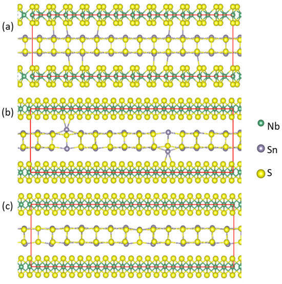
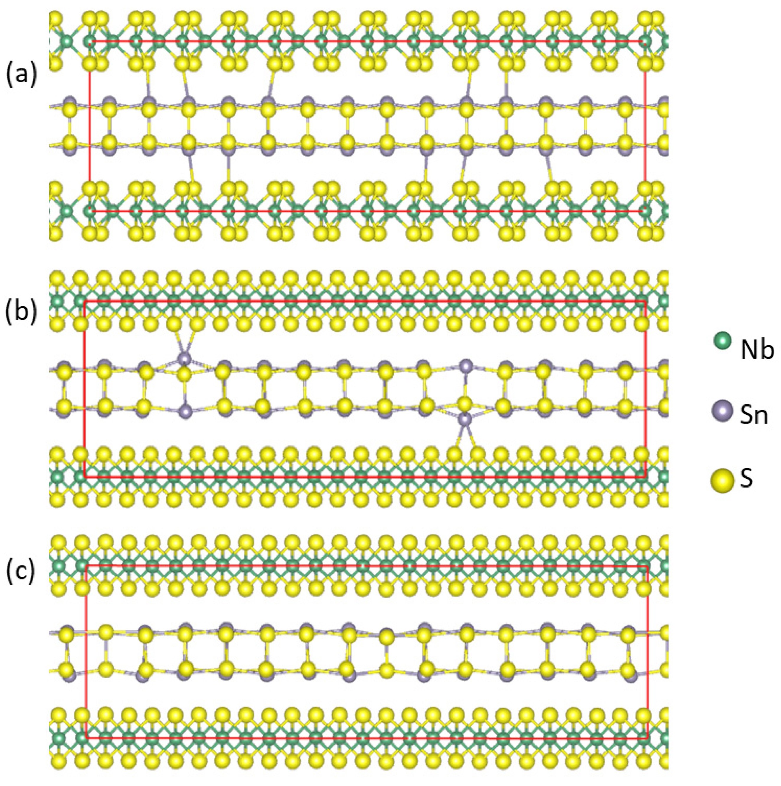
Figure 6.
Schematic structure of optimized atomic arrangements for (SnS)1.167NbS2 (a) for comparison, (SnS0.929)1.167NbS2 (b), and (Sn0.929S)1.167NbS2 (c). The interlayer bonds Sn-S(Nb) with lengths within 3.1 Å are shown.
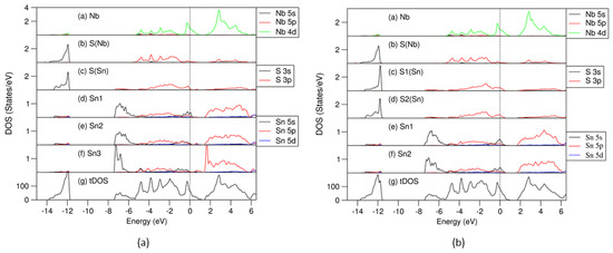
Figure 7.
Partial and total density of states curves for the atoms and cell of the S vacant in the (SnS) part of (SnS0.929)1.167NbS2 (a) and Sn vacant in the (SnS) part of (Sn0.929S)1.167NbS2 (b). The dotted lines represent the Fermi level at zero eV. In (a), Sn1 has five S(Sn) neighbors, Sn2 has four Sn-S(Sn) bonds and two Sn-S(Nb) neighbors, and Sn3 has four Sn-S(Sn) bonds and a short Sn-S(Nb) bond (2.82 Å). In (b), Sn1 has five Sn-S(Sn) bonds, and Sn2 has five Sn-S(Sn) and two Sn-S(Nb) bonds. S1(Sn) has four Sn neighbors, and S2(Sn) has five Sn neighbors.
The influence of the S deficiencies in the (SnS0.929)1.167NbS2 approximant revealed the short Sn-S(Nb) bonds (Figure 6b). The Sn atoms near the S vacancies may have one or two S(Nb) neighbors with bond lengths varying between 2.8 Å and 3.2 Å. In comparison, the Sn-S(Nb) bond lengths range from 3.06 Å to 3.25 Å in the approximant (SnS)1.167NbS2 (Figure 6a). Meanwhile, the analysis showed that for the Sn deficiency configuration, (Sn0.929S)1.167NbS2, the shortest interlayer Sn-S(Nb) bond length is over 3.1 Å, as shown in Figure 6c, indicating weaker interlayer interactions.
The Bader charge analysis revealed slightly more electron loss for the Sn atoms (0.90 e/Sn) in the Sn-deficient approximant, (Sn0.929S)1.167NbS2 (Table S5), than in the S-deficient compound (0.87 e/Sn) (Table S6). This is reasonable considering the Sn/S(Sn) ratio in the ionic model. Meanwhile, the electrons in the atomic spheres (Table S7) show moderate variation for each species from the corresponding ones in the parental and the vacancy-free misfit layer compound, indicating charge transfers outside the spheres. Figure 7 shows the calculated partial density of states for selected atoms in and total density of states of the (SnS) part of the (SnS0.929)1.167NbS2 (a) and (Sn0.929S)1.167NbS2 (b) misfit layer compounds.
The frame of the DOS curves for both the S- (Figure 7a) and Sn-deficient (Figure 7b) systems are similar to that of the stoichiometric system (Figure 4): the S 3s states are in the range from −13.8 eV to −11.5 eV; the valence bands are in the range from −7.5 to 1.0 eV. The Fermi level is dominated by Nb 4d states. The lone Sn 5s2 pair splits into two parts.
One is at the lower part (−7.5 eV to −5.5 eV), related to Sn 5s bonding. The other is positioned at the upper parts of the valence bands (−1.5 eV to 0.2 eV), belonging to antibonding. There is a gap between the valence band and the conduction band. Meanwhile, there are also some subtle differences between the electronic properties of the S- or Sn-deficient compounds and those of the stoichiometric compound.
As shown in Figure 7a, in the S-deficient (SnS0.929)1.167NbS2 approximant, there are some unoccupied antibonding 5s orbitals of the Sn1 with five S(Sn) neighbors, while Sn2 atoms with four S(Sn) and one short Sn-S(Nb) bond (bond length is 2.82 Å) and Sn3 with four S(Sn) neighbors are almost fully occupied. It is also notable that there is a sharp bonding peak at around −7.0 eV for the Sn3 5s states. The S(Sn) 3p states in the valence bands in the S-deficient configurations are below the Fermi level. These results indicate that S deficiency in SnS induces electron filling of the S 3p states and enhances interlayer bonding.
In Figure 7b, in the Sn-deficient (Sn0.929S)1.167NbS2 approximant, both Sn1 and Sn2 with different numbers of S neighbors have some unoccupied antibonding Sn 5s states. The Fermi level is also in the middle of the S(Sn) 3p states. Meanwhile, the S(Nb) 3s states in the valence band are below the Fermi level, indicating weaker interlayer interactions.
4. Conclusions
The first-principles calculations revealed the dependence of the formation energy on the misfit parameter x for the (SnS)1+xNbS2 approximants. The most stable approximant has x = 0.167, close to the experimentally observed (SnS)1.171NbS2. The Bader charge analysis found a moderate charge transfer (0.18 e/NbS2) from the SnS layer to the NbS2 tri-layer part via the interlayer van der Waals interactions. S or Sn deficiencies in the SnS part have influences on the local bonding and interlayer interactions. There are short Sn-S(Nb) interlayer bonds formed in the S-deficient system, which enhances the interlayer interactions. Meanwhile, for the Sn-deficient (Sn0.929S)1.17NbS2, the interlayer Sn-S(Nb) bonding becomes weaker.
Supplementary Materials
The following supporting information can be downloaded at https://www.mdpi.com/article/10.3390/cryst14090756/s1: Table S1: Designed approximants and related symmetry for the (SnS)1+xNbS2 (x = 0.20, 0.167, 0.143) misfit compounds. * Pseudo-orthorhombic unit cells. The experimental values are included for comparison; Table S2: Calculated results (coordinates of atoms, interatomic distances, and Bader charges at the atomic sites) using the DFT + vdW approach for the (SnS)1.20NbS2 misfit layer compound, case (a). Table S3: Calculated results (coordinates of atoms, interatomic distances, and Bader charges at the atomic sites) using the DFT + vdW correction for the (SnS)1.167NbS2 misfit layer compound, case (b); Table S4: Calculated results (coordinates of atoms, interatomic distances, and Bader charges at the atomic sites) using the DFT + vdW correction for the (SnS)1.143NbS2 misfit layer compound, case (d); Table S5: Calculated results (coordinates of atoms, interatomic distances, and Bader charges at the atomic sites) using the DFT + vdW correction for the (Sn1−xS)1.167NbS2 (x = 0.071) misfit layer compound, case (e); Table S6: Calculated results (coordinates of atoms, interatomic distances, and Bader charges at the atomic sites) using the DFT + vdW correction for the (SnS1−x)1.167NbS2 (x = 0.071) misfit layer compound, case (f); Table S7: Calculated electronic configurations within the atomic spheres of the parent binary compounds and the misfit layer compounds, (Sn1−xS)1.167NbS2 (x = 0.00), case (b) and (x = 0.0714), case (e).
Funding
Financial support from EPSRC (UK) under grant number EP/S005102/1 is gratefully acknowledged.
Data Availability Statement
The original contributions presented in the study are included in the article/Supplementary Materials, further inquiries can be directed to the corresponding author/s.
Conflicts of Interest
The author declares no conflicts of interest.
References
- Wiegers, G.A.; Meetsma, A.; van Smaalen, S.; Hannge, R.J.; Wulff, J.; Zeinstra, T.; de Boer, J.L.; Kuypers, S.; van Tendeloo, G.; van Landuyt, J.; et al. Misfit layer compounds (MS)nTS2 (M = Sn, Pb, Bi, rare earth elements; T = Nb, Ta; n = 1.08–1.19), a new class of layer compounds. Solid State Commun. 1989, 70, 409–413. [Google Scholar] [CrossRef]
- Meerschaut, A. Misfit layer compounds. Curr. Opin. Solid State Mater. Sci. 1996, 1, 250–259. [Google Scholar] [CrossRef]
- Rouxel, J.; Meerschaut, A.; Wiegers, G.A. Chalcogenid misfit layer compounds. J. Alloys Compd. 1995, 229, 144–157. [Google Scholar] [CrossRef]
- Wiegers, G.A. Misfit layer compounds: Structures and physical properties. Prog. Solid State Chem. 1996, 24, 1–139. [Google Scholar] [CrossRef]
- Ng, N.; McQueen, T.M. Misfit layered compounds: Unique, tunable heterostructured materials with untapped properties. APL Mater. 2022, 10, 100901. [Google Scholar] [CrossRef]
- Leriche, R.T.; Palacio-Morales, A.; Campetella, M.; Tresca, C.; Sasaki, S.; Brun, C.; Debontridder, F.; David, P.; Arfaoui, I.; Šofranko, O.; et al. Misfit layer compounds: A platform for heavily doped 2D transition metal dichalcogenides. Adv. Funct. Mater. 2020, 31, 2007706. [Google Scholar] [CrossRef]
- Zullo, L.; Marini, G.; Cren, T.; Calandra, M. Misfit layer compounds as ultratunable field effects transistors: From charge transfer control to emergent superconductivity. Nano Lett. 2023, 23, 6658–6663. [Google Scholar] [CrossRef] [PubMed]
- Nader, A.; Briggs, A.; Gotoh, Y. Superconductivity in the misfit layer compounds (BiSe)1.10(NbSe2) and (BiS)1.11(NbS2). Solid state Commun. 1997, 101, 149–153. [Google Scholar] [CrossRef]
- Huang, S.T.; Bai, J.H.; Long, H.Y.; Yang, S.C.; Chen, W.W.; Wang, Q.Y.; Sa, B.S.; Guo, Z.Y.; Zheng, J.Y.; Pei, J.J.; et al. Thermally activated photoluminescence induced by tunable interlayer interaction in naturally occurring van der Waals superlattice SnS/TiS2. Nano Lett. 2024, 24, 6061–6068. [Google Scholar] [CrossRef] [PubMed]
- Merrill, D.R.; Moore, D.B.; Bauers, S.R.; Falmbigl, M.; Johnson, D.C. Misfit layer compounds and ferecrystals: Model systems for thermoelectric nanocomposites. Materials 2015, 8, 2000–2029. [Google Scholar] [CrossRef] [PubMed]
- Lorenz, T.; Joswig, J.-O.; Seifert, G. Two-dimensional and tubular structures of misfit compounds: Structural and electronic properties Beilstein. J. Nanotechnol. 2014, 5, 2171–2178. [Google Scholar] [CrossRef]
- Serra, M.; Tenne, R. Nanotubes from misfit layered compounds. J. Coord. Chem. 2018, 71, 1669–1678. [Google Scholar] [CrossRef]
- Sreedhara, M.B.; Bukvišová, K.; Khadiev, A.; Citterberg, D.; Cohen, H.; Balema, V.; Pathak, A.K.; Novikov, D.; Leitus, G.; Kaplan-Ashiri, I.; et al. Nanotubes from the misfit layered compound (SmS)1.19TaS2: Atomic structure, charge transfer, and electric properties. Chem. Mater. 2022, 34, 1838–1853. [Google Scholar] [CrossRef]
- Lemon, M.; Harvel, F.G.; Gannon, R.N.; Lu, P.; Rudin, S.P.; Johnson, D.C. Targeted synthesis of predicted metastable compounds using modulated elemental reactants. J. Vac. Sci. Technol. A 2023, 41, 022203. [Google Scholar] [CrossRef]
- van Smaalen, S. A superspace group description of the misfit layer structure of (SnS)1.17(NbS2). J. Phys. Condens. Matter 1989, 1, 2791–2800. [Google Scholar] [CrossRef]
- Jobst, A.; van Smaalen, S. Intersubsystem chemical bonds in the misfit layer compounds (LaS)1.13TaS2 and (LaS)1.14NbS2. Acta Crystallogr. B 2002, 58, 179–190. [Google Scholar] [CrossRef]
- Fan, H.F.; van Smaalen, S.; Lam, E.J.W.; Beurskens, P.T. Direct methods for incommensurate intergrowth compounds. I. determination of modulation. Acta Cryst. A 1993, 49, 704–708. [Google Scholar] [CrossRef]
- Shen, X.; Chen, D.; Zhao, H.F.; Yao, Y.; Liu, X.Y.; Yu, R.C. Misfit-layered compound PbTiS3 with incommensurate modulation: Transmission electron microscopy analysis and transport properties. Chin. Phys. B 2013, 22, 116102. [Google Scholar] [CrossRef]
- Meerschaut, A.; Guemas, L.; Auriel, C.; Rouxel, J. Preparation, structure determination and transport properties of a new misfit layer compound: (PbS)114(NbS2)2. Eur. J. Solid State Inorg. Chem. 1990, 27, 557–570. [Google Scholar]
- Wiegers, G.A.; Haange, R.J. Electric transport and magnestic properties of the misfit layer compound (LaS)1.14NbS2. J. Phys. Condens. Matter 1990, 2, 455–463. [Google Scholar] [CrossRef]
- Sourisseau, C.; Cavagnat, R.; Tirodo, J.L. A Raman study of the misfit layer compounds, (SnS)1.17NbS2 and (PbS)1.18TiS2. J. Ramman Spectrosc. 1992, 23, 647–651. [Google Scholar] [CrossRef]
- Fang, C.M.; Ettema, A.R.H.; Haas, C.; Wiegers, G.A.; van Leuken, H.; de Groot, R.A. Electronic structure of the misfit-layer compound (SnS)1.17NbS2 deduced from band-structure calculations and photoelectron spectra. Phys. Rev. B 1995, 52, 2336–2347. [Google Scholar] [CrossRef] [PubMed]
- Krasovskki, E.E.; Tiedje, O.; Schottke, W.; Brandt, J.; Kanzow, J.; Rossnagel, K.; Kipp, L.; Skibowski, M.; Hytha, M.; Winkler, B. Electronic structure and UPS of the misfit chalcogenide (SnS)NbS2 and related compounds. J. Electron Spectrosc. Relat. Phenom. 2001, 114–116, 1133–1138. [Google Scholar] [CrossRef]
- Göhler, F.; Mitechson, G.; Alemayehu, M.B.; Speck, F.; Wanke, M.; Johnson, D.C.; Seyller, T. Charge transfer in (PbSe)1+δ(NbSe2)2 and (SnSe)1+δ(NbSe2)2 ferecrystals investigated by photoelectron spectroscopy. J. Phys. Condens. Matter 2018, 30, 055001. [Google Scholar] [CrossRef] [PubMed]
- Fang, C.M.; van Smaalen, S.; Wiegers, G.A.; Haas, C.; de Groot, R.A. Electronic structure of the misfit layer compound (LaS)1.14NbS2: Band-structure calculations and photoelectron spectra. J. Phys. Condens. Matter 1996, 8, 5367–5382. [Google Scholar] [CrossRef]
- Chikina, A.; Bhattacharyya, G.; Curcio, D.; Sanders, C.E.; Bianchi, M.; Lanatà, N.; Watson, M.; Cacho, C.; Breholm, M.; Hofmann, P. One-dimensional electronic states in a natural misfit structure. Phys. Rev. Mater. 2002, 6, L092001. [Google Scholar] [CrossRef]
- Fang, C.M.; Wiegers, G.A.; Haas, C. Charge transfer and photoemission spectra of some later rare earth misfit layer compounds, (LnS)1+xTS2 (Ln = Tb, Dy, Ho; T = Nb, Ta). Phys. Condens. Matter 1997, 233, 134–138. [Google Scholar] [CrossRef]
- Beekman, M.; Heideman, C.L.; Johnson, D.C. Ferecrystals: Non-epitaxial layered intergrowths. Semicond. Sci. Technol. 2014, 29, 064012. [Google Scholar] [CrossRef]
- Reisinger, G.R.; Richter, K.W. Review of vanadium-based layered compounds. J. Alloys Compd. 2021, 891, 161976. [Google Scholar] [CrossRef]
- Deudon, C.; Lafond, A.; Leynaud, O.; Moëlo, Y.; Meerschaut, A. Quantification of the interlayer charge transfer, via bond valence calculation, in a 2D misfit compounds: The case of (Pb(Mn,Nb)0.5S1.5)1.15NbS2. J. Solid State Chem. 2000, 155, 1–8. [Google Scholar] [CrossRef]
- Gotoh, Y. Structural stability and charge transfer of (SnS0.93)1.17NbS2 by accurate modelling of incommensurate composite crystal structure using information criterion. J. Phys. Soc. Jpn. 2021, 90, 094601. [Google Scholar] [CrossRef]
- Brandt, J.; Kanzow, J.; Roßbagl, K.; Kipp, L.; Skibowski, M.; Krasovskii, E.; Schattke, W.; Traving, M.; Stettner, J.; Press, W.; et al. Band structure of the misfit compound (PbS)NbS2 compared to NbSe2: Experiment and theory. J. Electron Spec. Relat. Phenom. 2001, 114–116, 555–561. [Google Scholar] [CrossRef]
- Kabliman, E.; Blaha, P.; Schwarz, K. Ab initio study of stabilization of the misfit layer compound (PbS)1.14TaS2. Phys. Rev. B 2010, 82, 125308. [Google Scholar] [CrossRef]
- Abramov, S.P. Varieties of charge transfer and bonding between layers in misfit layer compounds (MX)xTX2. J. Alloys Compd. 1997, 259, 212–218. [Google Scholar] [CrossRef]
- Fang, C.M.; de Groot, R.A.; Wiegers, G.A.; Haas, C. Band structure calculations and photoemission spectra of (SnS)1.20TiS2. J. Phys. Condens. Matter 1996, 8, 1663–1667. [Google Scholar] [CrossRef]
- Fang, C.M.; de Groot, R.A.; Wiegers, G.A.; Haas, C. Electronic structure and evidence for La vacancies in the misfit layer compound (LaS)1.20CrS2. J. Phys. Chem. Solids 1997, 58, 1103–1109. [Google Scholar] [CrossRef]
- Cario, L.; Johrendt, D.; Lafond, A.; Felser, C.; Meerschaut, A.; Rouxel, J. Stability and charge transfer in the misfit layer compound, (LaS)(SrS)0.2CrS2: Ab initio band-structure calculations. Phys. Rev. B 1997, 55, 9409–9414. [Google Scholar] [CrossRef]
- Wiegers, G.A.; Meetsma, A.; Haange, R.J.; de Boer, J. Structure and physical properties of (SnS)1.18NbS2, ‘‘SnNbS3’’, a compound with misfit layer structure. Mater. Res. Bull. 1988, 23, 1551–1559. [Google Scholar] [CrossRef]
- Meetsma, A.; Wiegers, G.A.; Haange, R.J.; de Boer, J.L. The incommensurate misfit layer structure of (SnS)1.17NbS2, ‘SnNbS3’: I. A study by means of X-ray diffraction. Acta Cryst. A 1989, 45, 285–291. [Google Scholar] [CrossRef]
- Ohno, Y. Electronic structure of the misfit layer compounds PbTiS3 and SnSbS3. Phys. Rev. B 1991, 44, 1281–1291. [Google Scholar] [CrossRef] [PubMed]
- Klimes, J.; Bowler, D.R.; Michelides, A. Chemical accuracy for the van der Waals density functional. J. Phys. Condens. Matter 2010, 22, 022201. [Google Scholar] [CrossRef] [PubMed]
- Klimes, J.; Bowler, D.R.; Michelides, A. Van der Waals density functionals applied to solids. Phys. Rev. B 2011, 83, 195131. [Google Scholar] [CrossRef]
- Cowley, J.M.; Ibers, J.A. The structures of some ferric chloride-graphite compounds. Acta Cryst. 1956, 9, 421–431. [Google Scholar] [CrossRef]
- Kresse, G.; Hafner, J. Ab initio molecular-dynamics simulation of the liquid-metal-amorphous-semiconductor transition in germanium. Phys. Rev. B 1994, 49, 14251–14269. [Google Scholar] [CrossRef]
- Blöchl, P.E. Projector augmented-wave method. Phys. Rev. B 1994, 50, 17953–17978. [Google Scholar] [CrossRef] [PubMed]
- Perdew, J.P.; Burke, K.; Ernzerhof, M. Generalized gradient approximation made simple. Phys. Rev. Lett. 1996, 77, 3865–3868. [Google Scholar] [CrossRef]
- Fang, C.M.; Mohammadi, V.; Nihtianov, S.; Sluiter, M.F.H. Stability, geometry and electronic properties of BHn (n = 0 to 3) radicals on the Si(001)3×1:H surface from first-principles. J. Phys. Condens. Matter 2020, 32, 235201. [Google Scholar] [CrossRef]
- Monkhorst, H.J.; Pack, J.P. Special points for Brillouin-zone integrations. Phys. Rev. B 1976, 13, 5188–5192. [Google Scholar] [CrossRef]
- Wiedemeier, H.; von Schnering, H.G. Refinement of the structure of GeS, GeSe, SnS and SnSe. Z. Kristollogr. 1978, 148, 295–303. [Google Scholar] [CrossRef]
- von Schnering, H.G.; Wiedemeier, H. The high temperature structure of β-SnS and β-SnSe and the B16 to B33 type λ-transition path. Z. Kristollogr. 1981, 156, 143–150. [Google Scholar] [CrossRef]
- Ettema, A.R.H.F.; Groot, R.A.; Haas, C.; Turner, T.S. Electronic structure of SnS deduced from photoelectron spectra and band-structure calculations. Phys. Rev. B 1992, 46, 7363–7373. [Google Scholar] [CrossRef]
- Fisher, W.G.; Sienko, M.J. Stoichiometry, structure, and physical properties of niobium disulfide. Inorg. Chem. 1980, 19, 39–43. [Google Scholar] [CrossRef]
- Morosin, B. Structure refinement on NbS2. Acta Cryst. B 1974, 30, 551–552. [Google Scholar] [CrossRef]
- Jones, R.O. Density functional theory: Its origins, rise to prominence, and future. Rev. Mod. Phys. 2015, 87, 897–923. [Google Scholar] [CrossRef]
- Fang, C.M.; Wiegers, G.A.; Meetsma, A.; de Groot, R.A.; Haas, C. Crystal structure and band structure calculations of Pb1/3TaS2 and Sn1/3NbS2. Physica B 1996, 226, 259–267. [Google Scholar] [CrossRef]
- Bader, R.F.W. A quantum-theory of molecular-structure and its applications. Chem. Rev. 1991, 91, 893–928. [Google Scholar] [CrossRef]
- Bader, R.F.W. A bonded path: A universal indicator of bonded interactions. J. Phys. Chem. A 1998, 102, 7314–7323. [Google Scholar] [CrossRef]
Disclaimer/Publisher’s Note: The statements, opinions and data contained in all publications are solely those of the individual author(s) and contributor(s) and not of MDPI and/or the editor(s). MDPI and/or the editor(s) disclaim responsibility for any injury to people or property resulting from any ideas, methods, instructions or products referred to in the content. |
© 2024 by the author. Licensee MDPI, Basel, Switzerland. This article is an open access article distributed under the terms and conditions of the Creative Commons Attribution (CC BY) license (https://creativecommons.org/licenses/by/4.0/).