Article

The Nested Topological Band-Gap Structure for the Periodic Domain Walls in a Photonic Super-Lattice

by
Zhen Lai
1,2,
Yufu Liu
1,2,
Yunlin Li
1,2,
Xuezhi Wang
1,2 and
Xunya Jiang
1,2,3,*
1
Department of Light Sources and Illuminating Engineering, School of Information Science and Engineering, Fudan University, Shanghai 200433, China
2
Engineering Research Center of Advanced Lighting Technology, Fudan University, Ministry of Education, Shanghai 200433, China
3
Institute of Future Lighting, Academy for Engineering and Technology, Fudan University, Shanghai 200433, China
*
Author to whom correspondence should be addressed.
Crystals 2024, 14(9), 757; https://doi.org/10.3390/cryst14090757
Submission received: 12 August 2024 / Revised: 21 August 2024 / Accepted: 22 August 2024 / Published: 26 August 2024
(This article belongs to the Special Issue Topological Photonic Crystals)

Abstract

:
We study the nested topological band-gap structure of one-dimensional (1D) photonic super-lattices. One cell of the super-lattice is composed of two kinds of photonic crystals (PhCs) with different topologies so that there is a domain wall (DW) state at the interface between the two PhCs. We find that the coupling of periodic DWs could form a new band-gap structure inside the original gap. The new band-gap structure could be topologically nontrivial, and a topological phase transition can occur if the structural or material parameters of the PhCs are tuned. Theoretically, we prove that the Hamiltonian of such coupled DWs can be reduced to the simple Su–Schrieffer–Heeger (SSH) model. Then, if two super-lattices carrying different topological phases are attached, a new topological interface state can occur at the interface between the two super-lattices. Finally, we find the nested topological band-gap structure in two-dimensional (2D) photonic super-lattices. Consequently, such nested topological structures can widely exist in complex super-lattices. Our work improves the topological study of photonic super-lattices and provides a new way to realize topological interface states and topological phase transitions in 1D and 2D photonic super-lattices. Topological interface states in super-lattices are sensitive to frequency and have high accuracy, which is desired for high-performance filters and high-finesse cavities.

1. Introduction

Models of topologically nontrivial photonic crystals (PhCs) have aroused much interest for the past few years. In a similar way as controlling the passage of electrons in semiconductors, PhCs possess bands through which photons in certain frequency ranges can propagate and gaps that serve as regions of suppressed transmission [1,2]. With the development of topology and condensed matter physics, it was soon realized that topologies can also be applied to photonic systems, creating topological photonics [3]. When two PhCs with different topological properties are connected, an interface state that is topologically protected can serve as special current channels [3,4]. Many systems have been proposed to achieve the topological interface state [5,6], such as one-dimensional (1D) PhCs and high-dimensional PhCs with broken symmetry [7,8,9]. The topological interface state can be applied to the enhancement of nonlinear optical responses and to the topological protection of quantum correlation [8,10,11]. With the rapid development of photonics, different materials and structures such as phononic lattices and plasmonic crystals have been used as practical realizations of 1D super-lattice models [12,13,14]. In fact, with the continuous improvement of theories and experiments, many basic aspects or phenomena beyond the scope of ordinary electronic systems have been discovered. For instance, high-dimensional electromagnetic systems have been demonstrated to support the 1D interface state [15,16], and more complicated systems, such as Floquet insulators and nonlinearities, have also been reported [17,18,19,20]. Compared with high-dimensional systems, the existence of topological interface states in 1D models is more inspiring for understanding the basic topological principles and can be used as a basic model to get insight into more complex systems [21,22,23,24,25,26]. As is known to all, the simple 1D Su–Schrieffer–Heeger (SSH) model of polyacetylene polymer has been well studied and has provided the basic tool for studying super-lattice model and topological insulators [27,28]. If we consider the interface state as a localized atomic orbital, it is possible to use it as a foundation for constructing super-lattices. The super-lattices may manifest different topological phases and new interface states. The SSH model can be expressed by the tight-binding model of a chain with two sub-lattices. The topological interface states, also called the domain walls (DWs) [27,28,29,30], occur at the ends of a finite SSH model with an open boundary condition or the interfaces between two SSH models with different topologies.
One-dimensional super-lattices can also be considered as a platform to study the physical properties of coupled edge states [31]. For 1D plasmonic crystals, the realization of topological super-lattices and the associated interface states has been reported [13]. Furthermore, the evolution of resonant states in a photonic heterostructure composed of alternating binary and quaternary inversion-symmetric PhCs has been studied [1]. In addition, through the coupled mode theory, the coupling between a sequence of topological edge states in a super-lattice composed of stacked binary 1D PhCs with opposite topological properties has been verified, thus realizing the coupled-topological-edge-state waveguide modes [32]. However, the nested topological band-gap structure, which is formed by coupled DWs in photonic super-lattices, has never been studied to the best of our knowledge. In addition, the topological phase transition in the nested topological band-gap structure as well as some of the more interesting physical phenomena have also not been investigated in depth.
In this work, we systemically study the nested topological band-gap structure in 1D and two-dimensional (2D) PhC super-lattices. First, we show that the coupled periodic DWs can form a new band-gap structure inside the original PhC gap. Second, we find that the new band-gap structure is topologically nontrivial, and a topological phase transition can occur if we tune the parameters of the PhCs. Third, the model of coupled DWs can also be reduced into a new SSH model. If we attach two super-lattice models with different topological phases to each other, a topological interface state between the two super-lattices can be found. At last, we find that the nested topological band-gap structure can also be realized in 2D PhC super-lattices. Consequently, such nested topological band-gap structures can widely exist in many complex systems. Theoretically, our work improves the topological study of photonic super-lattices and provides a new way to realize topological interface states and topological phase transitions in 1D and 2D photonic super-lattices. Topological interface states in super-lattices are sensitive to frequency and have high accuracy, which is desired for high-performance filters and high-finesse cavities.

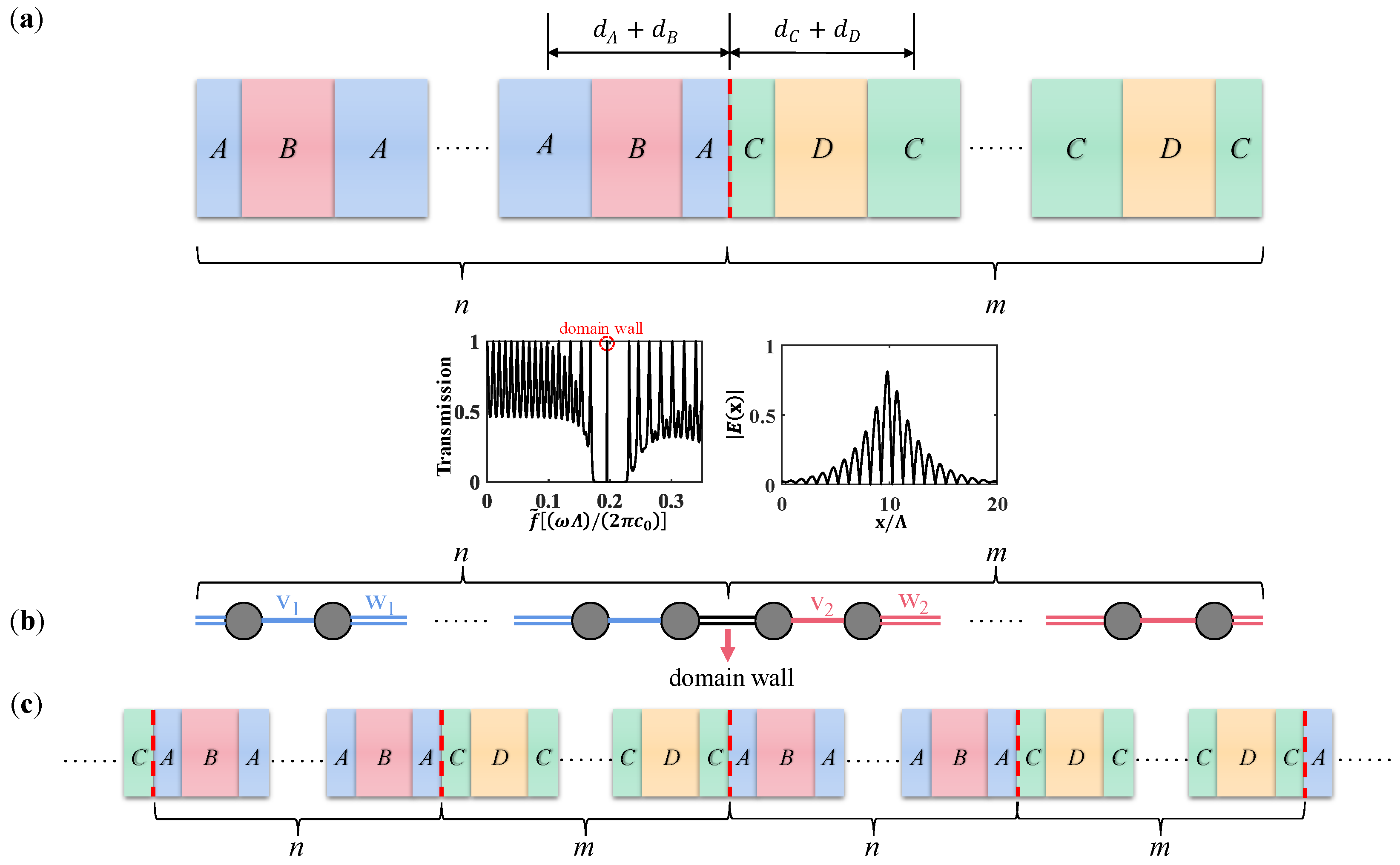
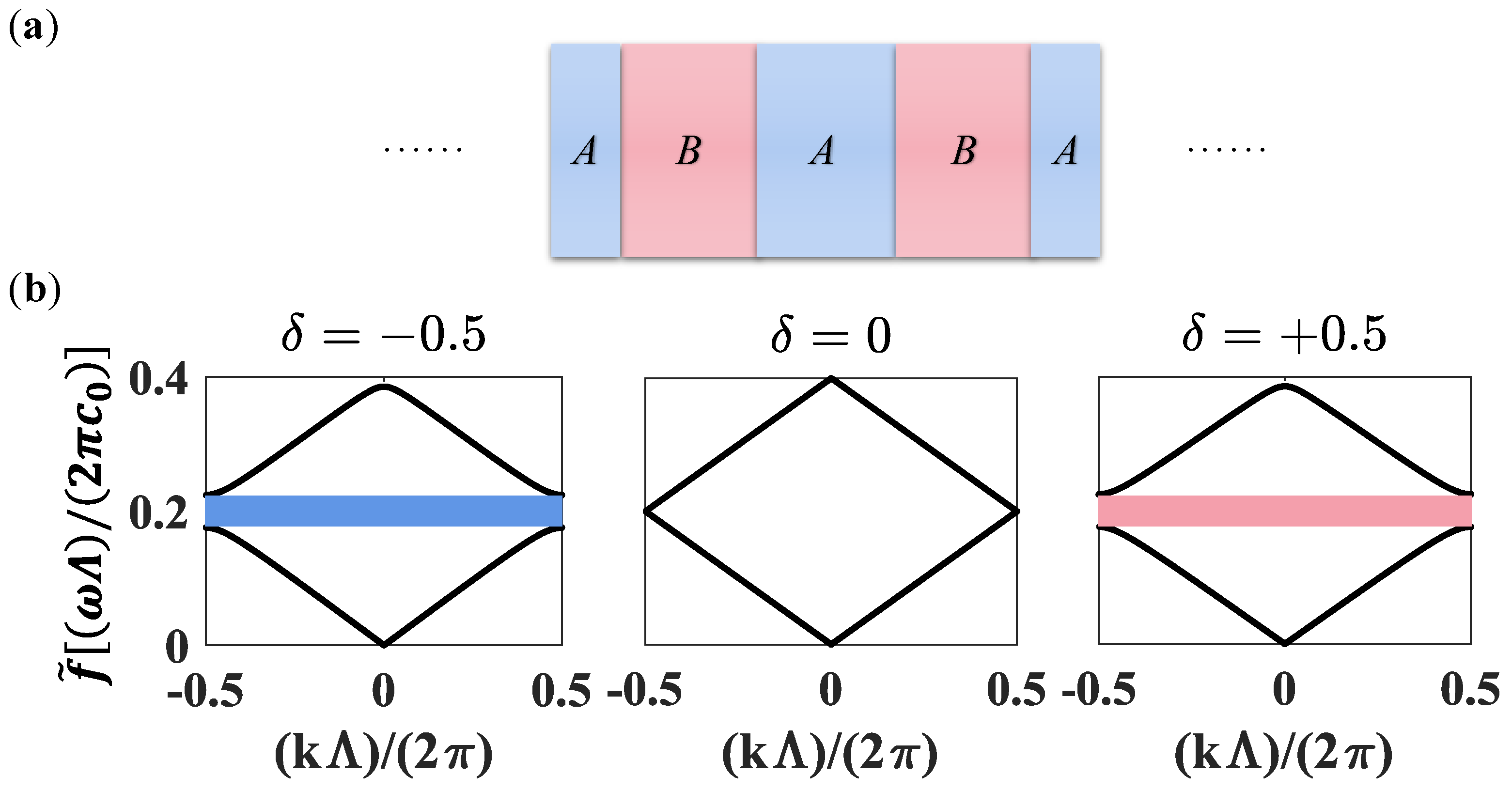
2. Model of 1D Super-Lattice

We introduce a 1D photonic super-lattice model with many cells, for which one cell is shown schematically in Figure 1a. There are n cells of AB-kind PhC on the left side and m cells of CD-kind PhC on the right side for a super-lattice cell. The interface between two kinds of PhCs is indicated by the dashed line in Figure 1a. The refractive indices and the widths of different layers are denoted by n A , n B , n C , and n D and d A / 2 , d B , d C / 2 , and d D , respectively. Without losing generality, the normalized thicknesses of four kinds of layers are supposed to be the same d A = d B = d C = d D = 0.5 Λ , where Λ is the thickness of a cell (the lattice constant) of both AB-kind and CD-kind PhCs. If two PhCs share the same gap range but have different topological properties, a topological interface state, which is also called the “domain wall”, will exist at the interface between the two PhCs [24]. Such a DW can be clearly seen from a sharp resonant peak inside the gap from the transmission spectrum of a super-lattice cell, and its field distribution | E ( x ) | is localized at the interface of two kinds of PhCs, which are shown in the insets of Figure 1a.
It is well known that such binary 1D PhCs can be thought of as photonic cases of the SSH model [33]. Then, a cell of our super-lattice model can also be presented in SSH model form, which is shown in Figure 1b. The single and double lines indicate intra-cell and inter-cell hopping terms. The blue lines signify v 1 and w 1 and the red lines signify v 2 and w 2 and are the intra-cell and inter-cell hopping terms of AB-kind and CD-kind PhCs, respectively. There is a DW if two SSH models have different topological properties.
In this work, we focus on the interaction of DWs of all cells of our super-lattice model. Since the DWs are deep inside the gap, their interaction is almost independent of all other states of the super-lattice model. The super-lattice model is shown in Figure 1c. All calculations in this work are done by the transfer matrix method (TMM) for 1D systems [34,35]:
E 1 + E 1 = M E n + 1 + 0 = M 11 M 12 M 21 M 22 E n + 1 + 0 ,
Based on the TMM, we can theoretically calculate the transmissions and bands of all 1D systems, such as structures with random layers or periodic systems.

3. Results and Analyses

In this section, we study the nested topological band-gap structure from our super-lattice model. First, we show that, not as generally expected, the interaction of periodic topological DWs can form a new band-gap structure inside the original gap. Second, we find that there is a topological origin for the new band-gap structure since the interaction of the DWs can be reduced into the SSH model. Third, we attach two super-lattice models with different topological phases to each other, and a topological interface state can be found. At last, we find the nested topological band-gap structure in 2D PhC super-lattices and realize the topological phase transitions and the topological interface state.

3.1. Disappearance of the Original DW and the New Band-Gap Structure of the Photonic Super-Lattice

In this subsection, we show that there are new band-gap structures from the interaction between DWs for our super-lattice model. Since the DW looks very like the defect state, one may naively imagine that many DWs generate a “domain wall band” similar to the “defect band” in a super-lattice model with periodic defects. However, we show that there are more complex and interesting phenomena for the DWs, such as the disappearance of the original DW and a nested topological band-gap structure generated by the coupled DWs.
We review the topological study [24] of a binary PhC as shown in Figure 2a. The refractive indices are set as n A = n ¯ δ , n B = n ¯ + δ , where n ¯ = 2.5 . As δ changes from 0.5 to 0 and then to + 0.5 , the evolutions of the band structure of AB-kind PhCs are as shown in Figure 2b, where the gap gradually shrinks until it closes at δ = 0 , and then it reopens afterwards. There is a topological phase transition at δ = 0 , and the red (blue) strip represents the topologically nontrivial (trivial) gap.
Then, we set n = m = 4 for a cell of the super-lattice model, as shown in Figure 1a, which means there are four cells of AB-kind and CD-kind PhCs at the left side and right side of a cell, respectively. We also choose δ 1 < 0 (trivial) and δ 2 > 0 (nontrivial) for the AB-kind and CD-kind PhCs. Meanwhile, to keep the gap centers of the AB-kind and CD-kind PhCs on both sides unchanged, we keep their total optical paths equal, i.e., n A d A + n B d B = n C d C + n D d D . Therefore, we can obtain the refractive index relation n A = n ¯ δ 1 , n B = n ¯ + δ 1 and n C = n ¯ δ 2 , n D = n ¯ + δ 2 , and we set δ 1 = 0.5 and δ 2 = + 0.6 .
We suppose the total cell number of our super-lattice model is N. Next, we can calculate the transmission spectra of our super-lattice model with different values of N, which are shown in Figure 3 for N from 1 to 5 and N = 10 . From Figure 3a, we can see that there is a DW inside the gap when N = 1 . As N gradually increases from two to five, some new states appear on both sides of the original DW, as shown in Figure 3a, and the number of new states increases with N. It looks like there will be a “domain wall band”, which agrees with our naive expectation. However, we are surprised to find that the central transmission peak of the original DW in Figure 3a gradually decreases with increasing N and finally almost disappears at N = 10 . Another interesting phenomenon is that when N increases by one, there are two new states, which are on either side of the original DW. This is against our intuition of the “domain wall band”, whose resonant peaks should increase by one state if N increases by one. The physical reasons behind these abnormal phenomena should be very interesting.
In order to find the reasons for the disappearance of the DW and the double new states appearing at the “domain wall band”, we calculate the band structure of the super-lattice at the normalized frequency range from 0.15 to 0.25 by cos ( k Λ ) = ( M 11 + M 22 ) / 2 [24], where k is the Bloch wave vector of the super-lattice model, and M 11 and M 22 are diagonal terms of the transfer matrix of a super-lattice cell.
Here, we calculate the band-gap structures when δ 2 = + 0.6 , + 0.5 , and + 0.4 , and the results are shown in Figure 4a. First, an interesting phenomenon we find is that instead of “one domain wall band”, there are two new bands and a small gap between them when δ 2 = + 0.6 . In other words, a new band-gap structure appears when DWs are coupled with each other. This is quite different from the case of one defect band formed for the super-lattice with periodic defects. The original DW in Figure 3a, whose transmission peak gradually disappears when we increase the cell number N of the super-lattice, is exactly at the center of the small gap. Hence, the new small gap is the reason for the disappearance of the transmission peak. The generation of a pair of new states at both sides of the original DW when N increases by one can be easily explained now. Since there are two new bands, with an increase of N by one, a new state will appear at each band.
Second, as seen in Figure 4a, for the changing of δ 2 from + 0.6 to + 0.4 , we can see that the new gap gradually shrinks until it closes at δ 2 = δ 1 = + 0.5 , and then it reopens. It is worth mentioning that when δ 2 = δ 1 = + 0.5 , the structure of CD-kind PhC is the same as the structure of AB-kind PhC, except that the position of the symmetry center changes from B to A. From every aspect, this gap-closing–reopening process is very similar to the topological phase transition of the SSH model. To verify this judgment, we observe the symmetry properties of the band-edge states. In Figure 4b, the field distribution of the four band-edge states that are signified in Figure 4a on the new lower band are shown. The dashed line is the symmetry center. We can see that the symmetry properties of the two band-edge states I and I I are different, while those of two band-edge states I I I and I V are the same. Such switching symmetry properties of band-edge states clearly show that it is a topological phase transition. In the 1D SSH model, an interface state will exist when the Zak phase of the occupied band on one side is different from that on the other side [24]. We also have calculated the Zak phase for each band [36], which is π for the δ 2 = + 0.6 and δ 2 = + 0.5 super-lattices but 0 for the δ 2 = + 0.4 super-lattice. We can see that there is a Zak phase jump for each band after the gap-closing–reopening process, which agrees with the symmetry properties of band-edge states naturally. Hence, we find an interesting phenomenon that the super-lattice of DWs that originate from the topological interface states between trivial and nontrivial PhCs can also generate topologically nontrivial band-gap structures. We call this phenomenon the nested topological band-gap structure.
The physical mechanism behind the nested topological band-gap structure is also very intriguing. Let us start with the analysis of the coupling between DWs. First, we know that the DW state is localized at the interface between an AB-kind PhC and a CD-kind PhC. We have calculated the decay length of the electric field for each side, which is 0.894 in the AB-kind PhC and 0.754 in the CD-kind PhC. Therefore, the field decays exponentially from the interface in the two kinds of PhCs. Second, the coupling strength between two neighbor DWs is from the overlapping integral of the fields of two DWs, as shown in Figure 5a. Obviously, the coupling strength mainly depends on the decay length of the DWs and the distance between two DWs. For our case, the distances between all DWs are the same since the lengths of the two kinds of PhCs are the same. However, as shown in Figure 5a, since the decay length of the DW field in the AB-kind PhC is different from the decay length of the DW field in the CD-kind PhC, the coupling strength for a DW to the right-side neighbor is different from that to the left-side neighbor. If we define the coupling strength over the AB-kind PhC as the intra-cell hopping term v and define the coupling strength over the CD-kind PhC as w , then the system of coupled DWs can be expressed as shown in Figure 5b, which is an exactly new SSH model. Hence, different decay lengths are the physical origin of the nested topological band-gap structure for our model.

3.2. Theory of Coupled DWs in the Photonic Super-Lattice Model

In this subsection, we show theoretically that the super-lattice with the nested topological band-gap structure can be reduced to the simple 1D SSH model, and the coupling constants of the corresponding SSH model can also be obtained. Therefore, our super-lattice model with the coupled DWs can have the nontrivial topological property since it is the same as the 1D SSH model.
From the results in the previous subsection, we know that DWs are localized states since the field decays exponentially in both AB-kind and CD-kind PhCs, as shown in Figure 5a. Therefore, DWs can be well-characterized by the tight-binding model. | I and | I I are used to represent the AB-CD type and CD-AB type of DWs. Obviously, they have the same on-site energy since they are spatially inversive to each other. We set the left boundary of a unit cell of the super-lattice as the origin of the coordinates, i.e., x = 0 . Therefore, the eigen-field of DWs can be expressed as [28]:
| I = α i = 1 n l I I , 2 l I , 1 exp ( d l I I , 2 d l I , 1 ) i 1 2 | i , A + α i = n + 1 2 n l I , 2 l I I , 1 exp ( d l I , 2 d l I I , 1 ) 2 n + 1 2 i | i , C ,
| I I = β i = 1 n l I I , 2 l I , 1 exp ( d l I I , 2 d l I , 1 ) n + 1 2 i | i , B + β i = n + 1 2 n l I , 2 l I I , 1 exp ( d l I , 2 d l I I , 1 ) i n 1 2 | i , D ,
where α and β are normalization constants, d is the normalized thickness of dielectric layers, l I , 1 and l I , 2 are the decay lengths of two sides of an AB–CD-type DW, and l I I , 1 and l I I , 2 are the decay lengths of two sides of CD–AB-type DWs, respectively. Obviously, l I , 1 = l I I , 2 , l I , 2 , and l I I , 1 for our super-lattice model.
Next, we derive the hopping terms between DWs. In the CD-kind PhC, the state | I is coupled with the | I I state on the right. Therefore, we can obtain the hopping term v by the overlapping integral of the field of the | I state on the left and the field of the | I I state on the right. Similarly, the hopping term w can be obtained by calculating the overlapping integral of the field of the | I state on the right and the field of the | I I state on the left.
To obtain the hopping terms, we first calculate the field distribution of the DWs. Second, the overlapping integrals at AB-kind and CD-kind PhCs can be obtained as:
u = 1 2 ε ( x ) [ E i * ( x ) E j ( x ) + E j * ( x ) E i ( x ) ] d x ,
If we focus on the topic of the nested topological band-gap structure in a very small frequency range by the coupling of DWs, the Hamiltonian of the super-lattice with N cells can be written as:
H S L e f f = j = 1 N ( v | I ( j ) I I ( j ) | + w | I ( j + 1 ) I I ( j ) | ) + h . c . ,
The Hamiltonian in Equation (5) has the same form as the traditional SSH model, as we expected. Topological phase transitions can occur depending on the coupling strength of v and w . The topological phase transition point is v = w : that is, the case where the structure of the CD-kind PhC is the same as the structure of the AB-kind PhC.
The hopping terms are obtained by Equation (4) when δ 2 increases from + 0.3 to + 0.7 , and the results are shown in Figure 6. We can see that v gradually decreases as δ 2 gradually increases, while w does the opposite. In addition, we can find that v > w when δ 2 = + 0.4 and v < w when δ 2 = + 0.6 . In other words, the super-lattice is topologically trivial when δ 2 = + 0.4 , while it is topologically nontrivial when δ 2 = + 0.6 . Moreover, the two curves intersect at δ 2 = + 0.5 , which means v = w at this point and it is the topological phase transition point. Obviously, the result is consistent with the previous one obtained from the field symmetry and Zak phase.
In summary, we have theoretically derived the SSH-like Hamiltonian of the model of coupled DWs, and the hopping terms are obtained by the overlapping integrals. We also show that the topological phase transition exists for the coupled DWs in such a super-lattice system.

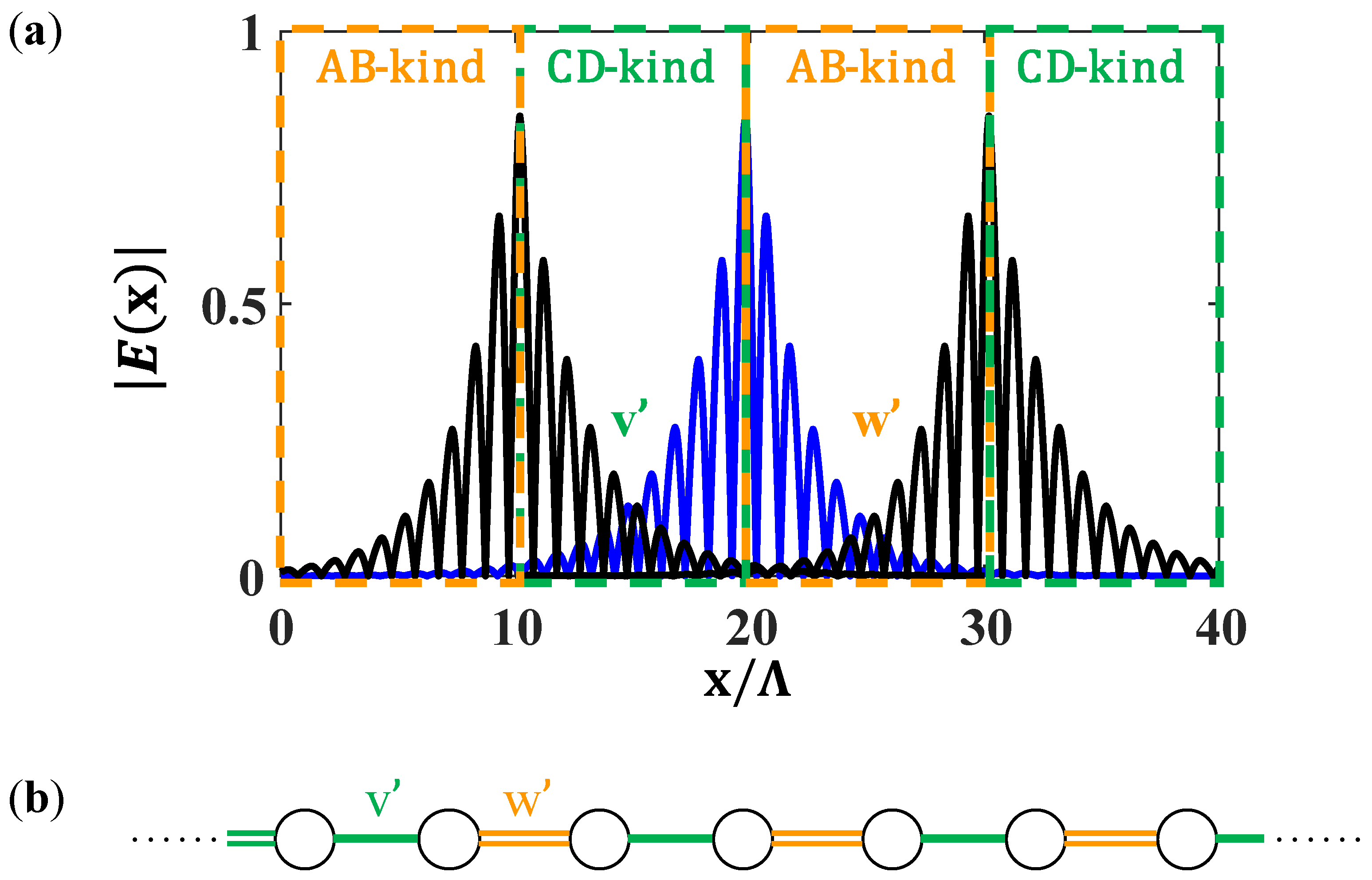
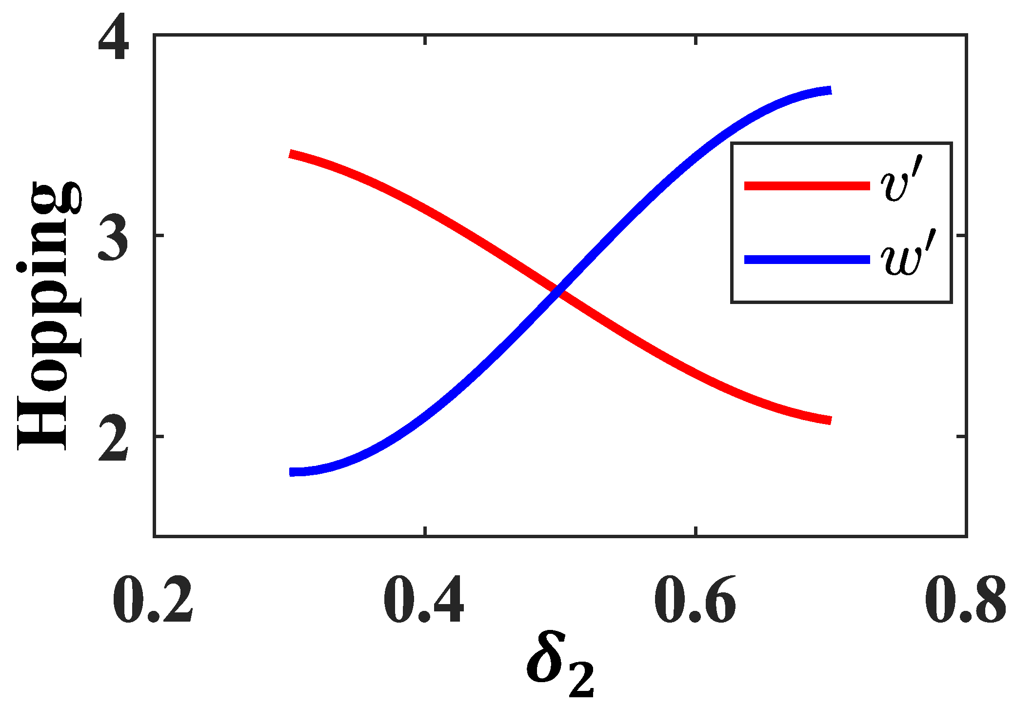
3.3. Topological Interface State between Two Photonic Super-Lattices

In this subsection, we attach two super-lattice models, which carry different topological phases for the coupled DWs. As we have predicted, there should be a new topologically protected interface state at the interface between two super-lattice models.
We choose δ 2 = + 0.4 (trivial) and δ 2 = + 0.6 (nontrivial) for two super-lattices to realize the topological interface state. The structure is shown in Figure 7a. We set the material parameters as n A = 3 , n B = 2 , n C 1 = 1.9 , n D 1 = 3.1 , n C 2 = 2.1 , and n D 2 = 2.9 and the cell number of the two super-lattices as p = q = 10 . The transmission spectra of the structure are shown in Figure 7b. We can see that there is a resonant peak with almost perfect transmission within the new gap of coupled DWs. To obtain the exponential decay lengths of the interface state, we calculate the absolute value of the electric field of the state, and we depict its cross-section profile in Figure 7c. The field of the state decays exponentially and symmetrically from the interface into two super-lattices, and the decay length of the interface state between the two super-lattices is also obtained as 63.033 Λ , which is much longer than the decay length of the DWs.

3.4. The Nested Topological Band-Gap Structure in a 2D Photonic Super-Lattice

In this subsection, we show that the nested topological band-gap structure can also appear for the 2D PhC super-lattices and is similar to that in 1D systems. The topological phase transitions and the new topological interface states in 2D PhC super-lattices can also be found.
One cell of the 2D PhC super-lattice model in the x-direction is shown schematically in Figure 8a and is composed of two kinds of 2D PhCs with the same square lattice but different symmetry centers. The regions of different colors represent dielectric materials with different refractive indices, which are denoted by n 1 , n 2 , n 3 , and n 4 . The lattice constant of the square lattice of PhCs is a 0 , and the edge size of the square rod in a PhC cell is 0.5 a 0 , as shown in Figure 8a.
The cell numbers of two 2D PhCs in one cell of super-lattice are the same and are set as four. As we expected, there will be a DW at the interface between the two PhCs since their topological properties are different. The DW is localized at the interface, and the field decays exponentially from the interface. To find the nested topological band-gap structure, we calculate the band-gap structure of the 2D super-lattice. We tune n 3 and n 4 while fixing n 1 = 4 and n 2 = 2 . Meanwhile, we keep their average refractive indices equal in order to leave the gap centers unchanged. We choose three sets of parameters as examples for our study, which are n 3 = 3.6 , n 4 = 2.5 ; n 3 = 4 , n 4 = 2 ; n 3 = 4.8 , and n 4 = 1.1 . The results are shown in Figure 8b–d. The red lines are the nested topological band-gap structure. From Figure 8b–d, we can see the gap-closing–reopening process. Obviously, a topological phase transition occurs in the 2D PhC super-lattice during the process of n 3 and n 4 change.
Therefore, we can obtain two 2D PhC super-lattices with trivial and nontrivial band topologies. We can attack the two super-lattices with different topological properties together, which have four cells for each 2D PhC super-lattice, to realize a topologically protected interface state. The states near the nested gap are shown in Figure 9a. We can see that there is a state in the gap, which is signified by the red circle. The absolute of the electric field distribution of this interface state is shown in Figure 9b. The inset of Figure 9b is a zoomed-in view of the topological interface state, which is well localized at the interface between the two 2D super-lattices.

4. Conclusions

In conclusion, we investigated the nested topological band-gap structure in photonic super-lattices. We showed that the coupling of periodic DWs could form a new band-gap structure inside the original gap, and the new band-gap structure could be topologically nontrivial. A topological phase transition can appear if we tune the structural or material parameters.
Furthermore, we proved theoretically that the Hamiltonian of such coupled DWs can be reduced to the SSH-like one. Then, we attached two super-lattices with different topological phases to each other to realize a new topological interface state. Finally, we found the nested topological band-gap structure in 2D photonic super-lattices. Consequently, we believe that such nested topological band-gap structures can exist widely in complex super-lattices. Theoretically, our work provides a new way to realize topological interface states and topological phase transitions in 1D and 2D photonic super-lattices. In practice, our model can be used to design photonic devices such as high-finesse photonic cavities and the edge-propagating channels of 2D super-lattices.

Author Contributions

Conceptualization, Z.L. and Y.L. (Yufu Liu); methodology, Z.L.; formal analysis, Z.L. and Y.L. (Yufu Liu); data curation, Z.L. and Y.L. (Yufu Liu); validation, Z.L., X.W. and Y.L. (Yunlin Li); writing, Z.L.; visualization, Z.L.; supervision, X.J. All authors have read and agreed to the published version of the manuscript.

Funding

This work is supported by National High Technology Research and Development Program of China (17-H863-04-ZT-001-035-01), the National Key Research and Development Program of China (2016YFA03001103, 2018YFA0306201), and the National Natural Science Foundation of China (grant No. 12174073).

Data Availability Statement

The original contributions presented in the study are included in the article, further inquiries can be directed to the corresponding author.

Conflicts of Interest

The authors declare no conflicts of interest.

References

  1. Bianchi, N.J.; Kahn, L.M. Optical states in a 1D superlattice with multiple photonic crystal interfaces. J. Opt. 2020, 22, 065101. [Google Scholar] [CrossRef]
  2. Yablonovitch, E. Inhibited spontaneous emission in solid-state physics and electronics. Phys. Rev. Lett. 1987, 58, 2059. [Google Scholar] [CrossRef] [PubMed]
  3. Lu, L.; Joannopoulos, J.D.; Soljačić, M. Topological photonics. Nat. Photonics 2014, 8, 821–829. [Google Scholar] [CrossRef]
  4. Amnon, Y.; Yeh, P. Optical Waves in Crystals: Propagation and Control of Laser Radiation; Wiley: New York City, NY, USA, 1984. [Google Scholar]
  5. Ma, G.; Xiao, M.; Chan, C.T. Topological phases in acoustic and mechanical systems. Nat. Rev. Phys. 2019, 1, 281–294. [Google Scholar] [CrossRef]
  6. Ling, C.; Xiao, M.; Chan, C.T.; Yu, S.F.; Fung, K.H. Topological edge plasmon modes between diatomic chains of plasmonic nanoparticles. Opt. Express 2015, 23, 2021–2031. [Google Scholar] [CrossRef]
  7. Gao, W.; Hu, X.; Li, C.; Yang, J.; Chai, Z.; Xie, J.; Gong, Q. Fano-resonance in one-dimensional topological photonic crystal heterostructure. Opt. Express 2018, 26, 8634–8644. [Google Scholar] [CrossRef]
  8. Peng, Y.; Xu, J.; Dong, H.; Dai, X.; Jiang, J.; Qian, S.; Jiang, L. Graphene-based low-threshold and tunable optical bistability in one-dimensional photonic crystal Fano resonance heterostructure at optical communication band. Opt. Express 2020, 28, 34948–34959. [Google Scholar] [CrossRef]
  9. Wu, L.H.; Hu, X. Scheme for achieving a topological photonic crystal by using dielectric material. Phys. Rev. Lett. 2015, 114, 223901. [Google Scholar] [CrossRef]
  10. Guo, J.; Wang, H.; Dai, X.; Xiang, Y.; Tang, D. Enhanced nonlinear optical responses of graphene in multi-frequency topological edge modes. Opt. Express 2019, 27, 32746–32763. [Google Scholar] [CrossRef]
  11. Dueñas, J.M.; Pérez, G.O.; Hermann-Avigliano, C.; Torres, L.E.F. Quadrature protection of squeezed states in a one-dimensional photonic topological insulator. Quantum 2021, 5, 526. [Google Scholar] [CrossRef]
  12. Li, E.; Eggleton, B.J.; Fang, K.; Fan, S. Photonic Aharonov–Bohm effect in photon–phonon interactions. Nat. Commun. 2014, 5, 3225. [Google Scholar] [CrossRef]
  13. Liu, C.; Ong, H. Realization of topological superlattices and the associated interface states in one-dimensional plasmonic crystals. Phys. Rev. B 2022, 106, 045401. [Google Scholar] [CrossRef]
  14. Xiao, Y.X.; Ma, G.; Zhang, Z.Q.; Chan, C.T. Topological subspace-induced bound state in the continuum. Phys. Rev. Lett. 2017, 118, 166803. [Google Scholar] [CrossRef] [PubMed]
  15. Cheng, X.; Jouvaud, C.; Ni, X.; Mousavi, S.H.; Genack, A.Z.; Khanikaev, A.B. Robust reconfigurable electromagnetic pathways within a photonic topological insulator. Nat. Mater. 2016, 15, 542–548. [Google Scholar] [CrossRef] [PubMed]
  16. Hafezi, M.; Mittal, S.; Fan, J.; Migdall, A.; Taylor, J. Imaging topological edge states in silicon photonics. Nat. Photonics 2013, 7, 1001–1005. [Google Scholar] [CrossRef]
  17. Peng, Y.G.; Geng, Z.G.; Zhu, X.F. Topologically protected bound states in one-dimensional Floquet acoustic waveguide systems. J. Appl. Phys. 2018, 123, 091716. [Google Scholar] [CrossRef]
  18. Liu, J.; Fu, L. Berry phase in nonlinear systems. Phys. Rev. A 2010, 81, 052112. [Google Scholar] [CrossRef]
  19. Elsayed, H.A.; Taha, T.; Algarni, S.A.; Ahmed, A.M.; Mehaney, A. Evolution of optical Tamm states in a 1D photonic crystal comprising a nanocomposite layer for optical filtering and reflecting purposes. Opt. Quantum Electron. 2022, 54, 312. [Google Scholar] [CrossRef]
  20. Elsayed, H.A. Transmittance properties of one dimensional ternary nanocomposite photonic crystals. Mater. Res. Express 2018, 5, 036209. [Google Scholar] [CrossRef]
  21. Wang, T.B.; Yin, C.P.; Liang, W.Y.; Dong, J.W.; Wang, H.Z. Electromagnetic surface modes in one-dimensional photonic crystals with dispersive metamaterials. JOSA B 2009, 26, 1635–1640. [Google Scholar] [CrossRef]
  22. Wang, X.; Liang, Y.; Wu, L.; Guo, J.; Dai, X.; Xiang, Y. Multi-channel perfect absorber based on a one-dimensional topological photonic crystal heterostructure with graphene. Opt. Lett. 2018, 43, 4256–4259. [Google Scholar] [CrossRef]
  23. Blanco-Redondo, A.; Andonegui, I.; Collins, M.J.; Harari, G.; Lumer, Y.; Rechtsman, M.C.; Eggleton, B.J.; Segev, M. Topological optical waveguiding in silicon and the transition between topological and trivial defect states. Phys. Rev. Lett. 2016, 116, 163901. [Google Scholar] [CrossRef]
  24. Xiao, M.; Zhang, Z.; Chan, C.T. Surface impedance and bulk band geometric phases in one-dimensional systems. Phys. Rev. X 2014, 4, 021017. [Google Scholar] [CrossRef]
  25. Xiao, M.; Ma, G.; Yang, Z.; Sheng, P.; Zhang, Z.; Chan, C.T. Geometric phase and band inversion in periodic acoustic systems. Nat. Phys. 2015, 11, 240–244. [Google Scholar] [CrossRef]
  26. Wang, F.; Song, X.Y.; Chio, U.; Wang, W.; Tang, X.H. Angular-adjustable single-channel narrow-band filter based on one-dimensional photonic crystal heterostructure. AIP Adv. 2021, 11, 095013. [Google Scholar] [CrossRef]
  27. Su, W.P.; Schrieffer, J.R.; Heeger, A.J. Solitons in polyacetylene. Phys. Rev. Lett. 1979, 42, 1698. [Google Scholar] [CrossRef]
  28. Asbóth, J.K.; Oroszlány, L.; Pályi, A. A short course on topological insulators. Lect. Notes Phys. 2016, 919, 166. [Google Scholar]
  29. Munoz, F.; Pinilla, F.; Mella, J.; Molina, M.I. Topological properties of a bipartite lattice of domain wall states. Sci. Rep. 2018, 8, 17330. [Google Scholar] [CrossRef]
  30. Liu, Y.; Xiong, L.; Jiang, X. The evolution of topological singularities between real-and complex-frequency domains and the engineering of photonic bands for Hermitian and non-Hermitian photonic crystals. New J. Phys. 2023, 24, 123042. [Google Scholar] [CrossRef]
  31. Xiong, L.; Zhang, Y.; Jiang, X. Resonance and topological singularity near and beyond zero frequency for waves: Model, theory, and effects. Photonics Res. 2021, 9, 2024–2036. [Google Scholar] [CrossRef]
  32. Wei, T.; Wang, Y. Coupled topological edge states in one-dimensional all-dielectric heterostructures. Opt. Express 2022, 30, 36900–36911. [Google Scholar] [CrossRef] [PubMed]
  33. Schmidt, C.; Palatnik, A.; Sudzius, M.; Meister, S.; Leo, K. Coupled topological interface states. Phys. Rev. B 2021, 103, 085412. [Google Scholar] [CrossRef]
  34. Markos, P.; Soukoulis, C.M. Wave Propagation: From Electrons to Photonic Crystals and Left-Handed Materials; Princeton University Press: Princeton, NJ, USA, 2008. [Google Scholar]
  35. Zhan, T.; Shi, X.; Dai, Y.; Liu, X.; Zi, J. Transfer matrix method for optics in graphene layers. J. Phys. Condensed Matter 2013, 25, 215301. [Google Scholar] [CrossRef] [PubMed]
  36. Wang, H.X.; Guo, G.Y.; Jiang, J.H. Band topology in classical waves: Wilson-loop approach to topological numbers and fragile topology. New J. Phys. 2019, 21, 093029. [Google Scholar] [CrossRef]
Figure 1. (a) The structure of the super-lattice model composed of AB-kind PhCs with n cells and CD-kind PhCs with m cells, respectively. The interface is indicated by the dashed line. The left inset shows the transmission spectra when n = m = 10 and n A = n D = 3 , n B = n C = 2 . There is a localized resonance with a sharp transmission peak at f ˜ [ ( ω Λ ) / ( 2 π c 0 ) ] 0.195143 . The right inset shows the absolute of the electric field | E ( x ) | at the transmission resonance. The field decays exponentially and symmetrically from the interface into two sides and has a decay length of 5.284 Λ . (b) The 1D SSH model. The single and double real lines between atoms indicate intra-cell and inter-cell hopping amplitudes, which are defined as v 1 , w 1 and v 2 , w 2 . (c) The super-lattice model.
Crystals 14 00757 g001
Figure 2. (a) The simplest structure of the AB-kind PhC. The refractive index of the material is n A = n ¯ δ , n B = n ¯ + δ , where n ¯ = 2.5 . (b) The diagram of the band structure (solid black curve) of AB-kind PhC changing with δ , where δ = 0.5 , 0, and + 0.5 . The blue and red strips represent the gap with different topological properties.
Crystals 14 00757 g002
Figure 3. (af) The transmission spectrum of the PhC super-lattice structure shown in Figure 1a when the total cell number N gradually increases from 1 to 5 and for N = 10 . Here, we set n = m = 4 , and δ 1 = 0.5 , δ 2 = + 0.6 .
Crystals 14 00757 g003
Figure 4. (a) The diagram of the band structure (solid black curve) of the PhC super-lattice changing with δ 2 , where δ 2 = + 0.6 , + 0.5 , and + 0.4 , while δ 1 = 0.5 remains unchanged. (b) The normalized field distribution of the points I, I I , I I I , and I V in (a). The dashed line is the symmetry center.
Crystals 14 00757 g004
Figure 5. (a) The field distribution of the DWs. (b) The dimerized domain walls form an SSH-like chain, and the intra-cell and inter-cell hopping terms are denoted by v and w .
Crystals 14 00757 g005
Figure 6. The hopping terms v and w calculating through the overlapping integral of the field with two DWs.
Crystals 14 00757 g006
Figure 7. (a) The structure composed of two kinds of super-lattice cells that possess different topological phases. The interface is indicated by the dashed line. Here, we take the PhC super-lattice structure shown in Figure 1a as the cell and set n = m = 4 . We set the material parameters as n A = 3 , n B = 2 , n C 1 = 1.9 , n D 1 = 3.1 , n C 2 = 2.1 , and n D 2 = 2.9 and the cell number of the two super-lattices as p = q = 10 . (b) The transmission spectra of the structure shown in (a) when p = q = 10 . There is a localized resonance with a sharp transmission peak at f ˜ [ ( ω Λ ) / ( 2 π c 0 ) ] 0.195018 . (c) The absolute value of the electric field at the transmission resonance. The field decays exponentially and symmetrically from the interface into two sides and has a decay length of 63.033 Λ .
Crystals 14 00757 g007
Figure 8. (a) One cell of the 2D PhC super-lattice model. (bd) The band structure of the 2D super-lattice with n 3 = 3.1 , n 4 = 2.3 ; n 3 = 4 , n 4 = 2 ; and n 3 = 4.9 , n 4 = 1.7 , respectively. Meanwhile, n 1 = 4 and n 2 = 2 remain the same. The red lines are the nested topological band-gap structure.
Crystals 14 00757 g008
Figure 9. (a) The band-gap of the structure composed of two 2D PhC super-lattices with trivial and nontrivial band topologies. The inset is a zoomed-in view of the surrounding topological interface state, and the red circle is the topological interface state. (b) The absolute of the electric field distribution of the topological interface state.
Crystals 14 00757 g009
Disclaimer/Publisher’s Note: The statements, opinions and data contained in all publications are solely those of the individual author(s) and contributor(s) and not of MDPI and/or the editor(s). MDPI and/or the editor(s) disclaim responsibility for any injury to people or property resulting from any ideas, methods, instructions or products referred to in the content.

