Abstract
Indium tin oxide (ITO) is a transparent conductive oxide (TCO) commonly used in the realization of optoelectronic devices needing at least a transparent electrode. In this work, ITO thin films were deposited on glass substrates by non-reactive RF magnetron sputtering, investigating the effects of power density, sputtering pressure, and substrate temperature on the electrical, optical, and structural properties of the as-grown films. High-quality films, in terms of crystallinity, transparency, and conductivity were obtained. The 120 nm thick ITO films grown at 225 °C under an argon pressure of 6.9 mbar and a sputtering power density of 2.19 W/cm2 without post-annealing treatments in an oxidizing environment showed an optical transmittance near 90% at 550 nm and a resistivity of cm. This material was applied as the electrode of simple-structure organic light-emitting diodes (OLEDs).
1. Introduction
Indium tin oxide (ITO) is one of the leading transparent conductive oxides (TCOs) and is extensively used for the electrodes of optoelectronic devices, including transparent and flexible ones, because the material possesses advantageous characteristics, such as high transmittance in the visible region of the spectrum, excellent conductivity, low light absorption, and high stability [1,2]. ITO is an inorganic mixture of indium oxide (In2O3) and tin oxide (SnO2), resulting in an n-type semiconductor characterized by a cubic bixbyite crystal structure [3]. It is commonly used in display technologies, solar cells, organic light-emitting diodes (OLEDs), and other applications for architectural and automotive purposes [4]. For typical high-quality ITO films suitable for use in applications, the transmittance must be higher than 80% in the wavelength range between 400 nm and 700 nm and the electrical sheet resistance below 10 [5,6]. In particular, for OLED application, the combination of good optical transparency and high electrical conductivity is highly desirable. Optical transparency in the visible spectrum ensures that the light produced by the organic layers within the OLED can pass through the electrodes with minimal loss, resulting in brighter and more efficient devices. Additionally, the electrical properties of ITO enable efficient charge injection into the organic layers, which promotes the recombination of electrons and holes that generate light. The low electrical resistance contributes to decreased power consumption and enhanced efficiency of the OLED device. ITO is compatible with a variety of substrates, including glass and flexible materials like plastic [7]. This makes it versatile for use in different types of OLED, from rigid screens or light sources to flexible ones, foldable displays, or wearable devices. The ability to be deposited on flexible substrates is particularly important, as the demand for innovative, flexible displays continues to grow. Various deposition techniques are used to obtain ITO thin films: thermal evaporation [8], chemical vapor deposition [9], pulsed laser deposition [10], spray pyrolysis [11], and DC (direct current) [12] and RF (radio frequency) magnetron sputtering [13]. It is well known that both optical properties and electrical properties are strongly dependent on the deposition process parameters, such as gas pressure, substrate heating during deposition, sputtering power, chamber environment, and post-deposition annealing treatment [14].
RF magnetron sputtering is the principal technique employed in industrial context to fabricate ITO films. This method provides accurate control of deposition parameters, making it appropriate for applications that require uniformity as well as high quality of thin films. Indeed, it provides several advantages over other methods, such as uniform material film over a large area, good repeatability, high deposition rate, reliable process stability, simple control of the film thickness, and suitability for large-scale manufacturing [15,16,17].
In RF magnetron sputtering, a target material is bombarded with high-energy ions produced in a plasma, usually consisting of argon gas. Ions displace atoms from the target, which then adhere to the substrate, creating a thin film. The procedure employs a radio frequency power source that usually functions at a frequency of 13.56 MHz. Moreover, in the deposition chamber, it is possible to intentionally introduce reactive gas species that can be included in the film during deposition [18]. Reactive magnetron sputtering, using oxygen as the reactive gas and argon as the sputtering gas, is often applied to deposit ITO [19,20]. However, this technique, especially when performed in transition mode [21], has the disadvantage of complex deposition processes because the target conditions rapidly vary with the quantity of reactive gas injected in the process chamber. Therefore, this technology, although it enables a high deposition rate and low energy consumption, requires appropriate systems to control the sputtering process in order to maintain stable deposition conditions during film growth [22]. Nevertheless, films deposited by using pure argon gas exhibit a significant lack of oxygen. The presence of oxygen vacancies within the ITO structure has a significant impact on its electrical conductivity. When ITO films are produced under oxygen-deficient conditions, the resulting vacancies generate free electrons, increasing the number of charge carriers in the film and enhancing its conductivity [23].
By introducing O2 during the process, the re-sputtering of the film is induced by the impact of high-energy oxygen atoms, and this reduces the number of oxygen vacancies in the structure of the film. However, a trade-off is needed, as higher oxygen concentration levels improve the transmittance of the final material, whereas the presence of oxygen vacancies increases its electrical conductivity [24,25].
Although ITO offers numerous benefits, it is not without challenges. Indium is a rare and costly material, and the fragility of ITO can restrict its use in highly flexible applications [26]. Continuing research is being conducted on alternate transparent conducting materials, such as conductive polymers or graphene, which could potentially supplement or even substitute ITO in the future; but currently, ITO continues to be the prevailing standard because of its unmatched mix of transparency, conductivity, and easy integration into existing manufacturing processes.
Organic light-emitting diodes are a well-known technology for display and light sources [27,28]. Their structure of stacked layers, for the several inner functions, therefore made of different materials [5,29,30], requires at least one transparent contact to out-couple the generated light. In this sense, as just said, there is an advantage to using ITO, which was employed even in the first work on efficient devices [31].
Taking into account all these aspects, in this study, ITO films were grown by the non-reactive RF magnetron sputtering method at various power densities, process pressures, and substrate temperatures. The aims were to develop a sustainable process for ITO deposition without using oxygen and to study the growth of the material films by exploring the relationship between the microstructure and the electrical and optical characteristics. In order to verify the obtained results, the in-house deposited ITO films were compared with commercial ITO on glass substrates through the manufacturing of organic light-emitting diodes (OLEDs) using ITO as the anode electrode.
2. Experimental Details
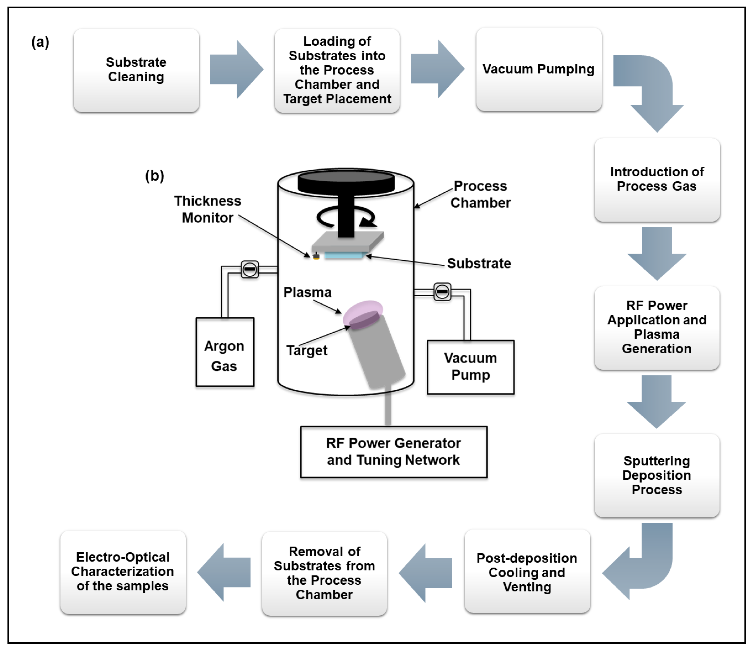
The ITO films were deposited onto 10 cm × 10 cm Corning Eagle XG® glass substrates by using a Kurt J. Lesker Company (KJLC, Hastings, UK) sputtering system with a KJLC Torus® HV magnetron sputter source. Figure 1b shows the schematic representation of the RF magnetron sputtering equipment used. All substrates were pre-cleaned with acetone and isopropanol in an ultrasonic bath for 60 min at 60 °C and dried in vacuum (≤ bar) at 150 °C for at least 1 h. A ceramic In2O3:SnO2 target (90:10 wt%, 99.99% purity) from KJLC was used. ITO target size was 3.0 inches in diameter and 1/8 inch in thickness. The radio frequency power (operating at 13.56 MHz) was provided by a generator matched to the target with a tuning network. Before each deposition process, the system was pumped down to a base pressure of mbar, and the target was pre-sputtered for 15 min by using the chosen sputtering condition. To ensure the homogeneity of the film, the substrate holder was rotated continually during the sputtering process. High-purity argon gas (99.999%) was used for the process. The diagram describing the complete process used for the realization of a film through the RF sputtering method is depicted in Figure 1a. Samples were deposited at different RF power densities (ranging from 1.10 to 3.07 W/cm2), at different sputtering pressures (from 1.5 mTorr to 15 mTorr), and considering different substrate temperatures (from room temperature up to 225 °C). Every process was stopped when the thickness monitor (a quartz crystal microbalance, whose tooling factor was previously calibrated) of the deposition chamber measured about 100 nm.
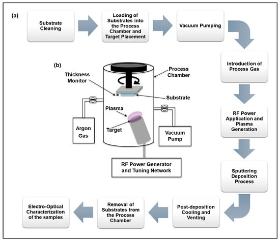
Figure 1.
(a) Diagram showing the procedure here adopted for making a film by using RF magnetron sputtering. (b) Schematic representation of the RF magnetron sputtering equipment used.
The thickness of the films was then determined by using a KLA-Tencor P10 stylus profilometer (KLA-Tencor Italy S.r.l, Italy). ITO resistivity was measured with a conventional four-point probe system Napson RESISTAGE RG-80 (Napson, Tokyo, Japan). The structural properties of the samples were analyzed by using an X-ray diffractometer PHILIPS X’PERT-MPD (now serviced by Malvern Panalytical S.r.l., Lissone, Italy). The crystallographic structures of the materials were measured by − 2 XRD, using CuK radiation, with a scan speed of 2°/min and a scan range from 20° to 80°. The optical properties were evaluated by employing a Perkin-Elmer Lambda 900 spectrophotometer (Perkin-Elmer Italia, Milano, Italy).
3. Results and Discussion
Table 1 summarizes the deposition parameters and the evaluated properties of the sputtered ITO thin films obtained at a fixed argon pressure of 15 mTorr, at different RF power densities and with the samples at room temperature. The thicknesses of all the films were in the range between 60 nm and 107 nm.

Table 1.
Deposition parameters and corresponding properties of ITO samples obtained at a fixed pressure of 15 mTorr, at different RF power densities and at room temperature.
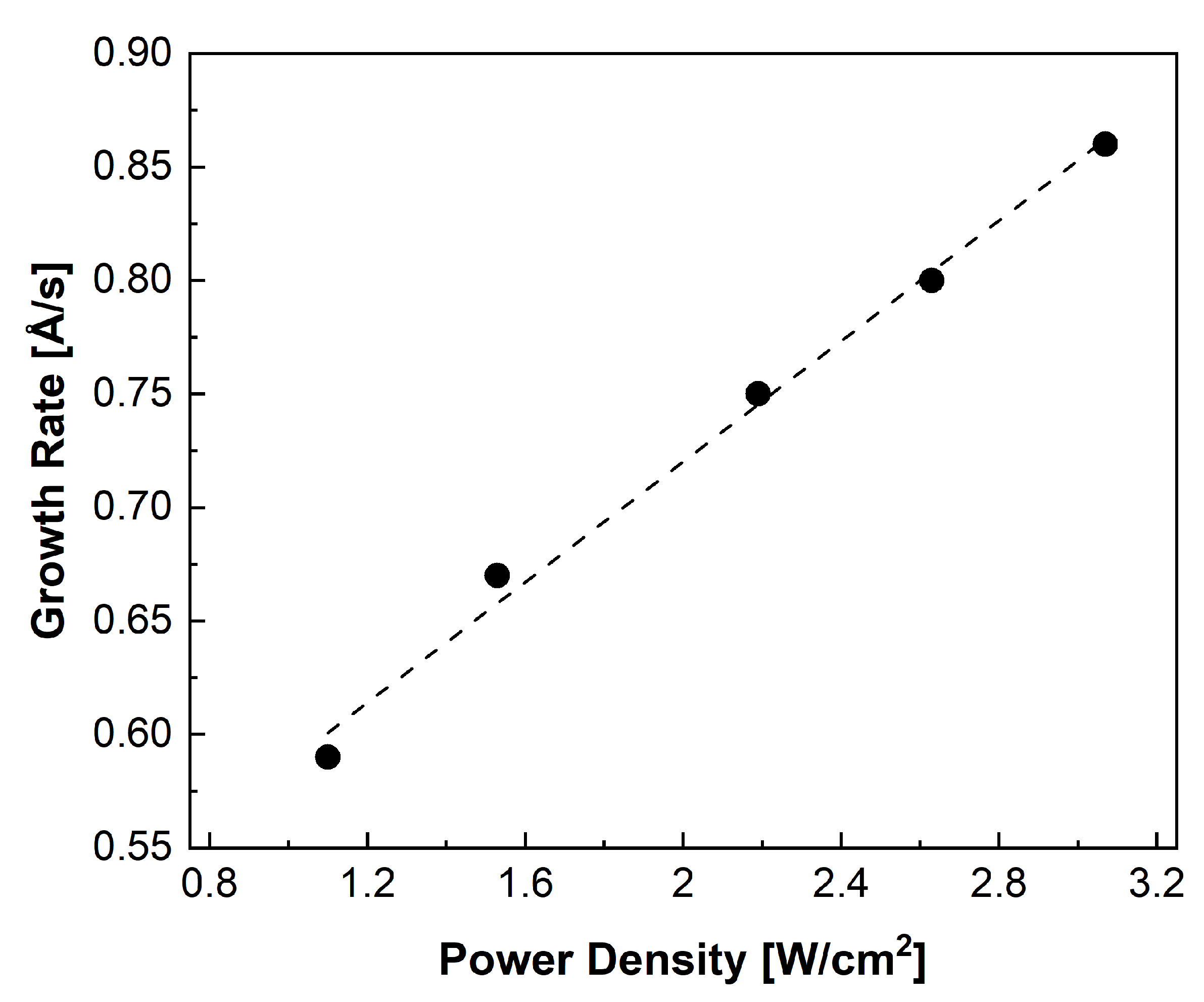
By fixing the argon pressure at 15 mTorr, the growth rate was found to be nearly linearly dependent on the RF sputtering power density, as reported in Figure 2. The phenomenon, also observed in [32,33], is linked to the increase in the kinetic energy of argon ions that occurs as the sputtering power increases. This, in turn, leads to an increase in the number of ions expelled from the target and subsequently deposited onto the substrate.
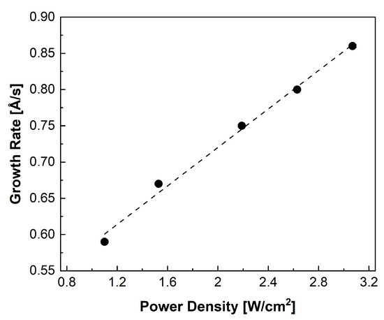
Figure 2.
ITO growth rate vs. RF power density. The argon pressure was fixed at 15 mTorr, and the process was at room temperature. The dashed black line is the linear fitting of the data.
Every deposition process was stopped when the thickness monitor inside the deposition chamber showed a value of 100 nm. The duration of the processes was recorded, and the effective growth rate was determined by measuring the obtained thickness of the ITO films against the process duration. According to the data presented in Table 1, the relation between film thickness and power density on the target exhibited a maximum value at a power density of 2.19 W/cm2 and subsequently dropped with the increase in power density. This phenomenon can be clarified by considering that sputtered particles acquire a significant amount of energy when the RF power is increased. Consequently, there is an increased probability that these particles will rebound off the substrate instead of adhering to it, as well as in more disordered paths. If this effect dominates over the growth rate increase resulting from the increase in power density, it could result in a thinner final film. Further investigation might be conducted by placing control samples adjacent to the substrate during the process and measuring the thickness of the resultant films.
The optical properties of the ITO films deposited at 15 mTorr at room temperature were investigated as a function of the power density. The measured transmittance spectra are shown in Figure 3. Apart from sample 1, which did not exhibit interference fringes due to the limited thickness [13] as a consequence of the low growth rate, all obtained ITO films deposited on glass substrates showed an average transmittance between 80% and 85% in the visible and NIR regions of the electromagnetic spectrum. Below 400 nm, the ITO films exhibited strong absorption due to sub-band and band-to-band absorption [34]. At 550 nm, the ITO film obtained at a power density of 2.19 W/cm2 showed the highest transmittance, equal to 82%, among the prepared ones (Figure 3).
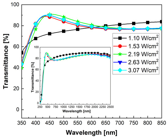
Figure 3.
UV–Vis region optical transmittance spectra of the ITO films deposited at different RF power densities, with an argon pressure of 15 mTorr and at room temperature. In the inset, the transmittance values measured for wavelengths between 250 and 2500 nm.
The correlation between the process parameters (RF sputtering power, process pressure, sputtering gas composition, sample and target temperature, eventual target bias, etc.) and transmittance is complex and relies on achieving an optimal equilibrium among layer thickness, surface smoothness, and structure. Low or high RF power density can have a detrimental effect on the ability of the film to transmit light. This is because it can lead to problems such as inadequate thickness, poor crystallinity, or increased surface roughness, all of which contribute to light scattering or absorption and decrease the transmittance of the film [35,36]. Based on the conducted studies, the power value of 2.19 W/cm2 can be considered the ideal sputtering power that achieves a balance among the thickness, crystallinity, and surface smoothness of the film.
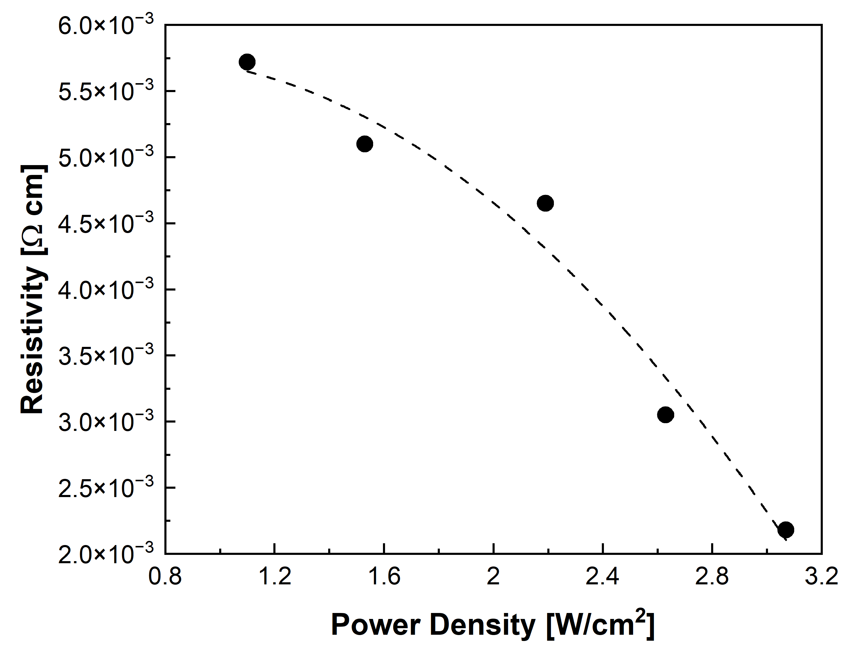
Additionally, the electrical characteristics of these samples were examined. Figure 4 illustrates the relationship between the resistivity of the films and the sputtering power density.
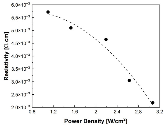
Figure 4.
Resistivity of the ITO films vs. the RF power density, deposited at room temperature and with an argon pressure of 15 mTorr.
It is observed that resistivity decreased as RF power density increased and reached a minimum value of Ω cm at 3.07 W/cm2, corresponding to a conductivity of about 459 S/cm. However, periodic arc flashes over the magnetron region were observed when the sputtering power density exceeded 2.19 W/cm2. For this reason, the next experiments were conducted at an RF power density of 2.19 W/cm2.
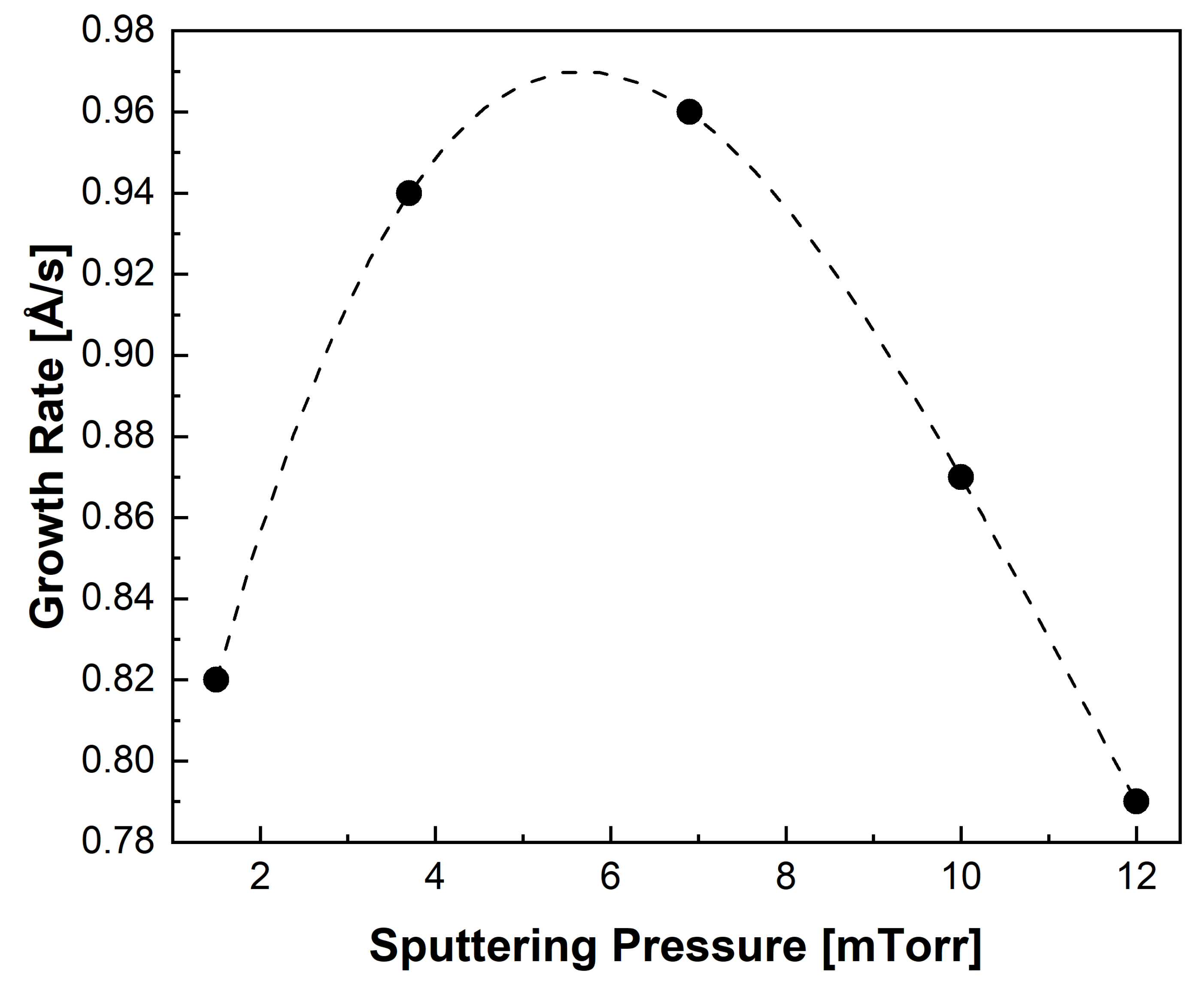
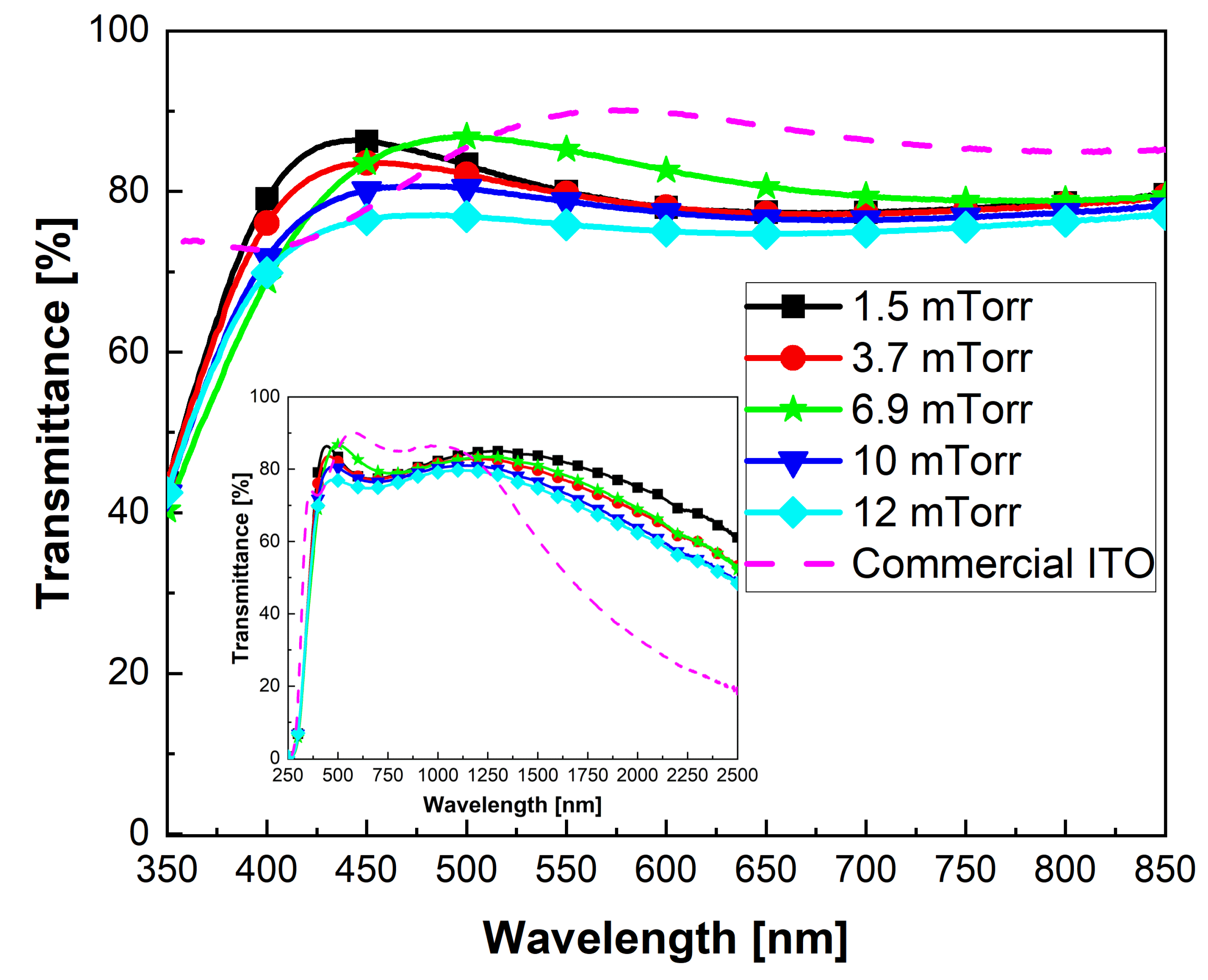
At the fixed power density of 2.19 W/cm2 while keeping the process at room temperature, samples were deposited at different sputtering pressures, and the corresponding properties were also evaluated. Figure 5 shows the relation between the growth rate of ITO and the pressure of argon. Among the tested argon pressures, the highest growth rate was observed at 6.9 mTorr. At higher pressures, the deposition rate decreased since there was an increase in the number of collisions between the sputtered particles and the argon atoms. Conversely, at low argon pressures, there was a decrease in the sputtering efficiency due to the low concentration of carrier near the magnetron region [37]. This means that an intermediate pressure exists where the growth rate is maximum [34]. Table 2 displays the deposition parameters together with the resulting thickness, growth rate, and resistivity of the obtained ITO thin films. The optical properties were also investigated as a function of the sputtering pressure. Figure 6 shows the optical transmittance of ITO films, having quite similar thickness, deposited on glass at different sputtering pressures and keeping a fixed power density of 2.19 W/cm2 and room temperature. Figure 6 also reports the transmittance curve of the commercial ITO on glass substrate, here used as reference, whose thickness was 150 nm. The ITO films deposited at 6.9 mTorr showed the highest transmittance (about 85%) in the visible region (at 550 nm) and an average transparency of 82% in the wavelength range from 400 nm to 800 nm. These values are close to those of the commercial ITO, which in turn exhibited a transmittance of 89% at 550 nm and an average transparency of 85% in the range from 400 to 800 nm. The obtained results have to be considered satisfactory, especially considering that these samples were fabricated with no oxygen addition during the process, which is able to increase the transparency of ITO thin films [38]. Regarding the specific influence of sputtering pressure on the optical properties of the ITO samples, the data presented in Figure 6 show that the average transmittance within the visible range of the spectrum was nearly 80% when the sputtering pressure was below 6.9 mTorr. Further pressure increases resulted in a decrease in the average transmittance, which was found to be 75% for the sample obtained at the pressure of 12 mTorr.
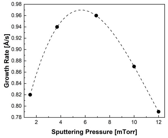
Figure 5.
ITO growth rate vs. argon pressure for films deposited at the fixed RF power density of 2.19 W/cm2 and at room temperature. The dashed line is the three-degree polynomial fit of the data.
Table 2.
Deposition parameters and properties of ITO samples obtained at different sputtering pressures, at fixed RF power density of 2.19 W/cm2 and at room temperature.
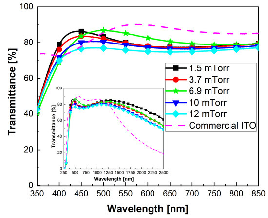
Figure 6.
UV–Vis region optical transmittance spectra of the ITO films obtained at different sputtering pressures with no heating during deposition. In the inset, the transmittance values measured for wavelengths between 250 and 2500 nm.
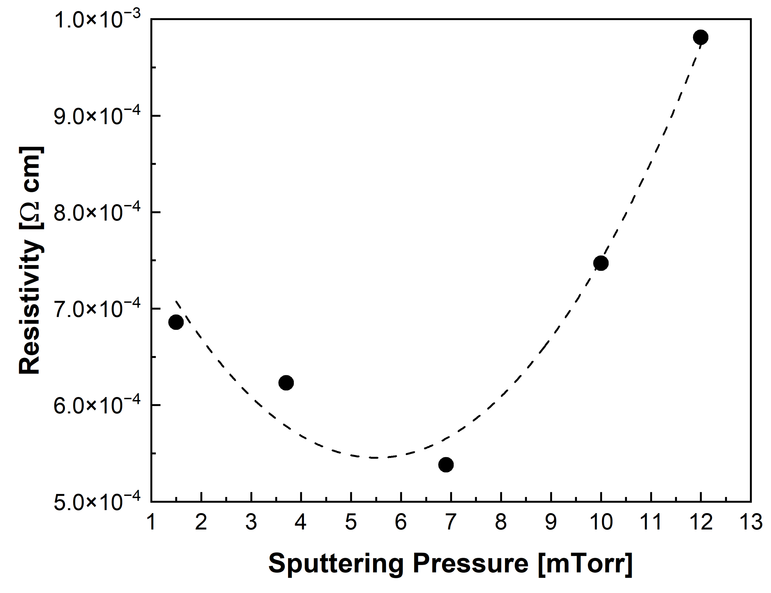
The electrical properties are also influenced by the sputtering pressure. It is possible to observe from Figure 7 that ITO thin films obtained at the sputtering pressure of 6.9 mTorr presented the minimum value of resistivity and, consequently, a high conductivity of about 1860 S/cm.
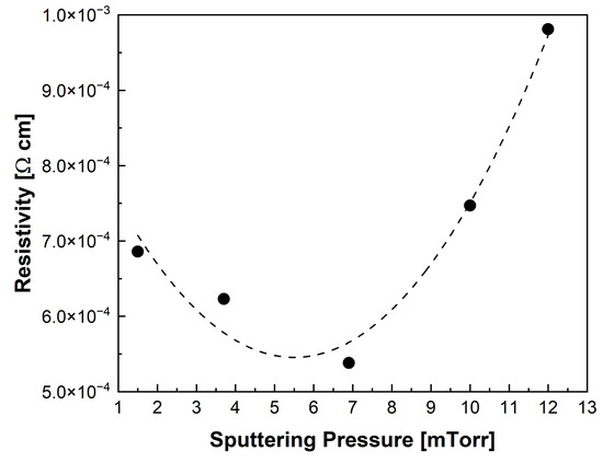
Figure 7.
Resistivity of the ITO films vs. sputtering pressure at a fixed power density of 2.19 W/cm2 and at room temperature.
Any other variation in the pressure led to worse electrical properties. This is mostly attributed to a decrease in mobility and carrier density, as also explained in [39].
It is worth highlighting that ITO films deposited at room temperature are typically amorphous [40,41]. Indeed, to enhance material crystallinity, samples were deposited by varying the deposition temperature and keeping the other process parameters (pressure and power density) fixed. In fact, during deposition, the mobility of atoms and clusters on the substrate, which is proportional to their energy, increases with the increase in the substrate temperature. Hence, substrate temperature influences the microstructure and the crystalline orientation of ITO films [42,43,44]. The properties of the films, such as resistivity, bandgap, and crystallinity, were evaluated at different substrate temperatures, varying from 25 °C to 225 °C (which is the maximum temperature that can be set in the sputtering system used here).
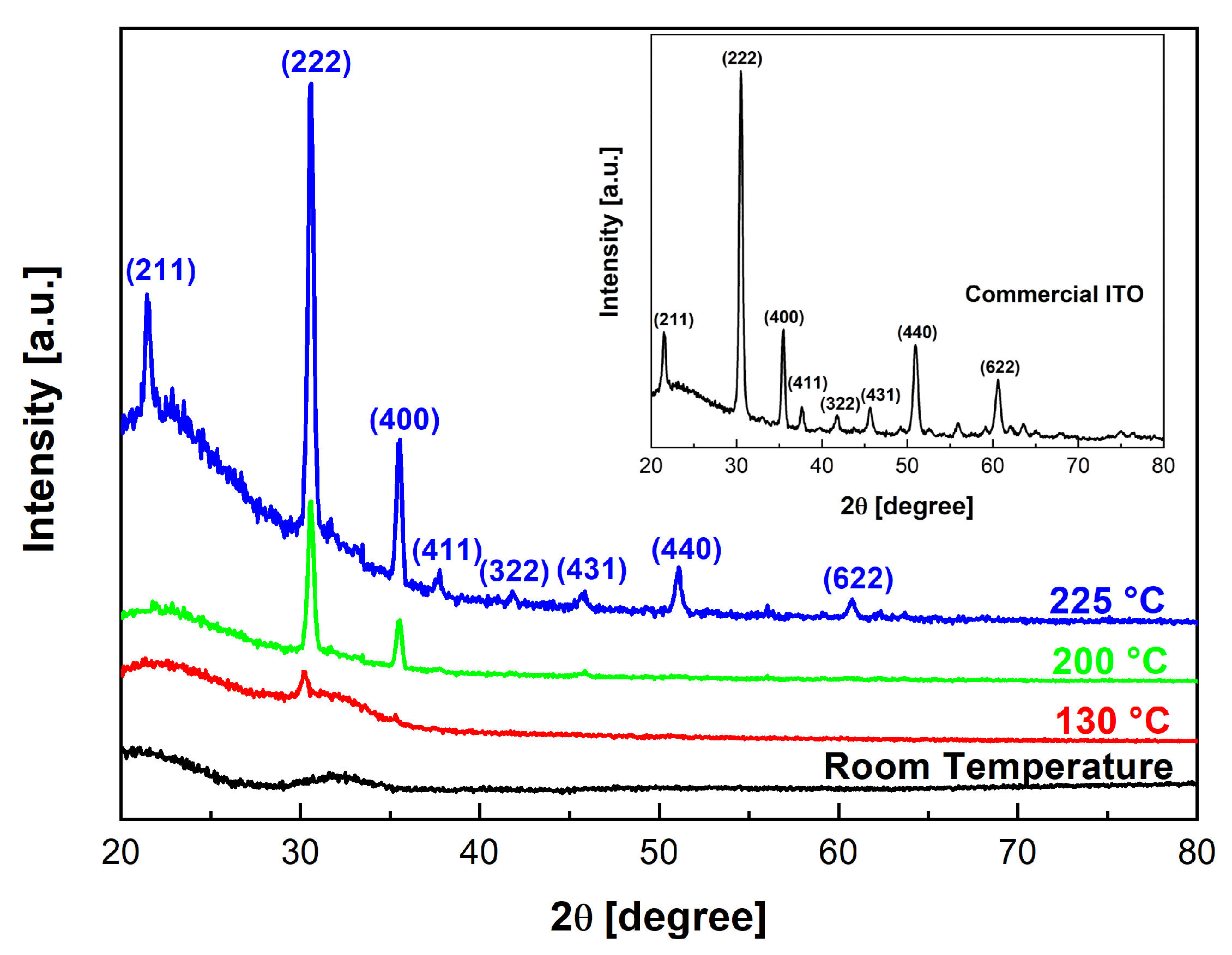
The analysis of the XRD patterns (Figure 8), shows a transition from an amorphous state to a polycrystalline state as the substrate deposition temperature increased. Films grown at substrate temperatures lower than 130 °C were amorphous, with a broad structure in the XRD spectrum. Crystallization was observed on the (222) plane at substrate temperatures ranging from 130 °C to 225 °C. This plane represents the preferred orientation of the films, and from a thermodynamic viewpoint, it corresponds to the plane with the lowest surface energy [45]. Others peaks, including the (211) and (400) ones, also appeared at high substrate temperatures. The observed orientation and diffraction peaks are characteristic of Sn-doped polycrystalline In2O3 thin films [44,46,47,48]. Similar crystallinity dependence was reported in [49], in which the authors observed changes in crystallization orientation with the increase in density power, which closely matches the changes documented in this study at the specified substrate temperatures. This behavior in crystalline growth can be clarified by the assertion made by Kumar and Mansingh. According to them, if the samples are obtained by the bombardment of more energetic particles and/or by particles that possess high energies upon reaching the growth surface, the (400) orientation can also become favored [50]. The inset of Figure 8 reports the XRD pattern of the commercial ITO, which shows the typical bixbyite structure (In2O3) (PDF card No. 006-0416) characterized by several peaks, also detected in the ITO samples here fabricated. It is worth noting that the data given in this work indicate that raising the substrate temperature is crucial to enhancing the crystallinity of the films. Due to their growth being induced by a non-reactive sputtering method, the presence of oxygen vacancies could potentially contribute to the changes in crystal orientation. Indeed, the number of oxygen vacancies is significantly influenced by the temperature of the substrate. This number can be expected to increase in the films obtained at high temperatures and in a no-added-oxygen deposition environment [51,52].
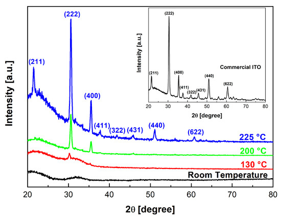
Figure 8.
X-ray diffraction patterns of 110 nm thick ITO films grown at various substrate temperatures, with sputtering pressure of 6.9 mTorr and power density of 2.19 W/cm2. In the inset, the X-ray diffraction pattern of commercial ITO.
The electrical properties of the films as a function of deposition temperature were also evaluated. In particular, Figure 9 illustrates a decrease in resistivity as the temperature of the substrate increased. The alteration in the preferred crystallization orientation may also have the beneficial effect of reducing the resistivity values in response to the increase in temperature. The lowest resistivity of Ω cm corresponding to a conductivity of 4763 S/cm was obtained at 225 °C for a 120 nm thick film. The increase in the conductivity of the films can be ascribed to the high level of crystallinity, leading to less scattering at the grain boundaries. This is a very important result, given that these films were not grown or annealed in an oxidizing environment. Furthermore, the obtained value of conductivity is very close to the commercial ITO’s (about 5500 S/cm), thus confirming the good quality of the ITO samples here fabricated.
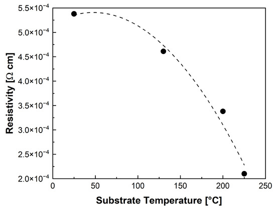
Figure 9.
Resistivity of the ITO films as a function of the substrate temperature, with sputtering pressure of 6.9 mTorr and power density of 2.19 W/cm2.
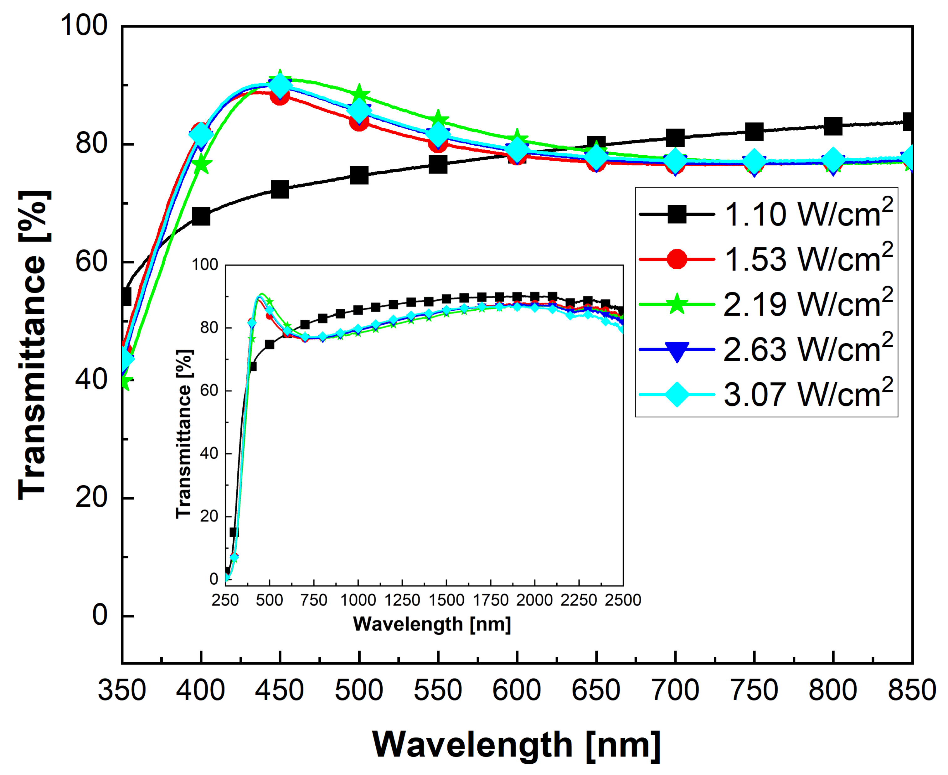
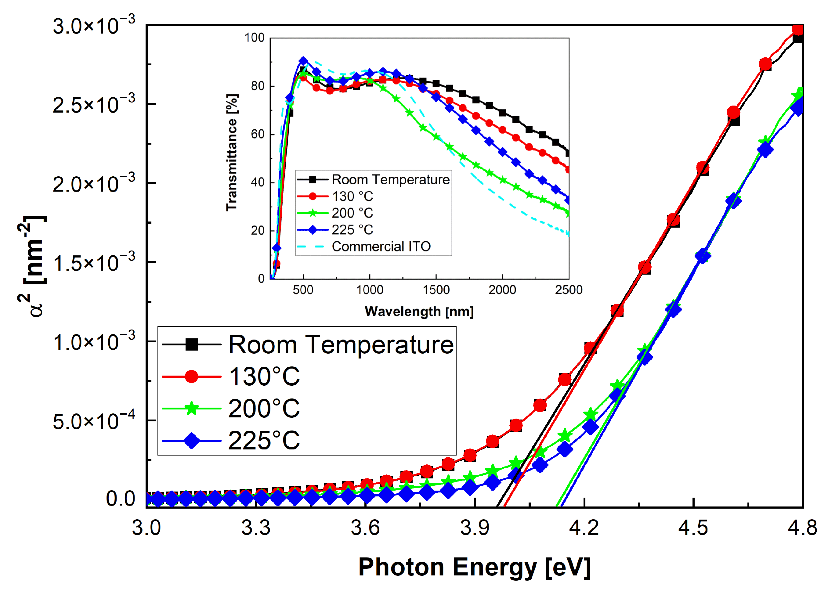
The optical transmission measurements performed on the films, reported in the inset of Figure 10, showed that in the range between 400 nm and 1100 nm, transmittance does not change much with the increase in substrate temperature, as reported in [53], remaining above 80%. In particular, the 120 nm thick film obtained at 225 °C showed a transparency equal to 89% at 550 nm and an average transparency of 85% in the range of wavelength between 400 and 800 nm, which are exactly the same values characterizing the commercial ITO. The high transparency in the visible region of the spectrum is a consequence of the wide bandgap of the obtained ITO films, which can be calculated from Equation (1) [52], that links the absorption coefficient with the transmittance T and the reflectance R of a film with a thickness t, plotting as a function of photon energy.
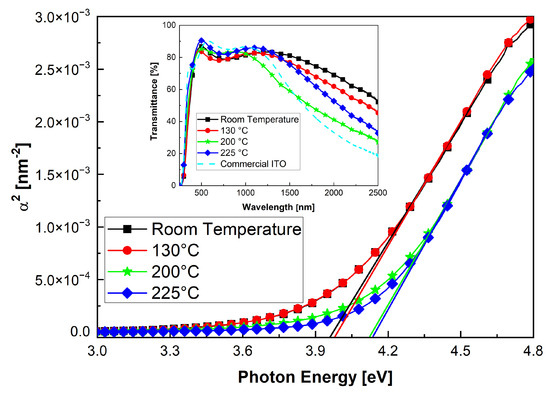
Figure 10.
Absorption coefficient vs. photon energy for ITO films grown at different substrate temperatures. The inset illustrates the transmission spectra of these films and of the commercial ITO.
The reflectance of conductive oxides is generally very low in the visible and UV ranges and can be neglected. Therefore, the following simplified formula can be used (Equation (2)).
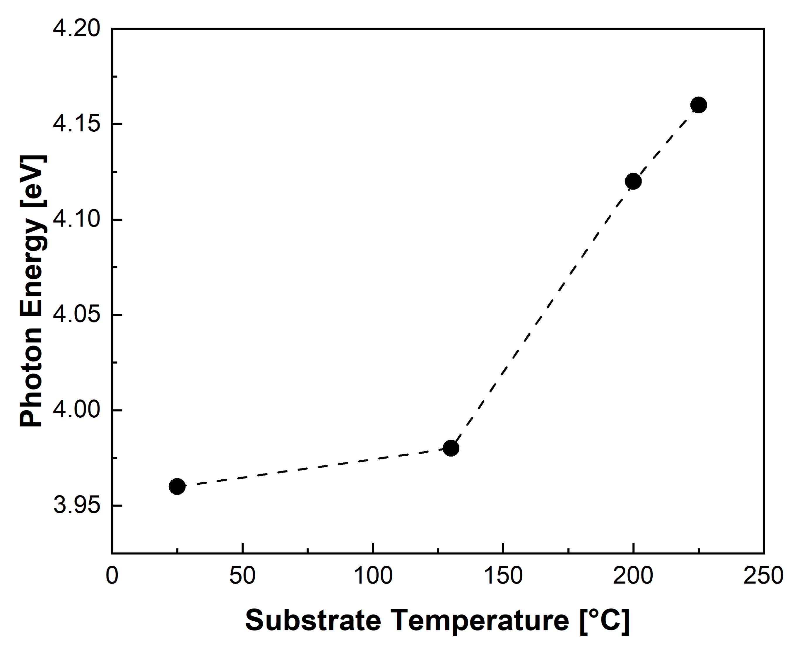
By extrapolating the linearly increasing part of the curve that shows the relationship between the absorption coefficient and photon energy, it is possible to determine the bandgap values of these films, as shown in Figure 10. The obtained values, ranging from about 3.95 eV to about 4.17 eV, show an increase in the bandgap value with respect to the substrate temperature increase, as also reported in Figure 11. The gradual increase in the deposition temperature results in an increase in the number of carriers that fill the lowest energy states in the conduction band, resulting in a bandgap widening, as explained by the Burstein–Moss shift model [51,54,55,56].
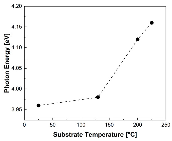
Figure 11.
Relationship between photon energy and substrate temperature during deposition of ITO thin films.
The ITO thin films with the best characteristics, deposited on glass by using a sputtering pressure of 6.9 mTorr, a power density of 2.19 W/cm2, and a deposition temperature of 225 °C, with thickness 120 nm, were used as the anodic material for organic light-emitting diodes. The devices had the structure shown in Figure 12a. A set of OLEDs, with the same structure, were also prepared by using commercial ITO (Delta Technologies, Ltd., Loveland, CO, USA; on Corning Eagle XG glass, with a substrate thickness of 1.1 mm). The commercial material had the following characteristics: thickness of 150 nm; sheet resistance of 12 , corresponding to a conductivity of 5556 S/cm; and a nominal transmittance of about 85% in the visible and NIR regions of the electromagnetic spectrum.
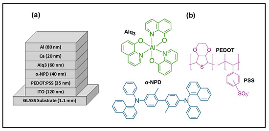
Figure 12.
(a) The structure of the prepared OLEDs with the anode electrode made of in-house sputtered and commercial ITO thin films. The commercial ITO film’s thickness was 150 nm. (b) The chemical structure of NPD, Alq3, and PEDOT:PSS.
Both types of ITO films were patterned through photolithography and chemical etching (HCl-based solution), followed by treatment with UV ozone. Commercial (Heraeus CleviosTM P VP AI 4083) poly(3,4 ethylenedioxythiophene):poly(styrenesulfonate) (PEDOT:PSS), which serves as a hole injection layer (HIL) to improve the injection of holes from ITO to the emitting layer, was deposited on the substrates by a spin-coating technique in air (3500 rpm for 60 s with an acceleration of 500 rpm/s). The coated substrate was then dried in an oven at 100 °C for a duration of two hours, resulting in a thickness of 35 nm.
The OLEDs were completed by thermally evaporating a 40 nm thick layer of N,N′-Di(1-naphthyl)-N,N′-diphenyl-(1,1′-biphenyl)-4,4′ diamine (-NPD, which acts as the hole transport layer (HTL)) and a 60 nm thick layer of tris(8 hydroxyquinolinate)aluminum (Alq3), used as both the emissive layer and as the electron transport layer (EML-ETL) (both -NPD and Alq3 were from Lumtec). The chemical structure of the organic material employed is shown in Figure 12b. Finally, Ca/Al cathode films (20 nm/80 nm) were evaporated on top of all the devices through a shadow mask to define the layout of the device, having a circular active area of 7 mm2. The evaporation processes were performed in a high-vacuum chamber at a base pressure of mbar and at rates below 1 Å/s.
The simple structure used for all these OLEDs ensures good reproducibility among the devices. It is important to highlight that a more complex structure and thickness optimization would be necessary to achieve higher device efficiency [57,58,59], but this is beyond the scope of this work.
The electro-optical measurements of the OLEDs were conducted within a glove box (H2O and O2 < 1 ppm) without device encapsulation. The devices were characterized through voltage–current measurements by using a Keithley 2400 SourceMeter (Tektronix Srl, Milano, Italy).
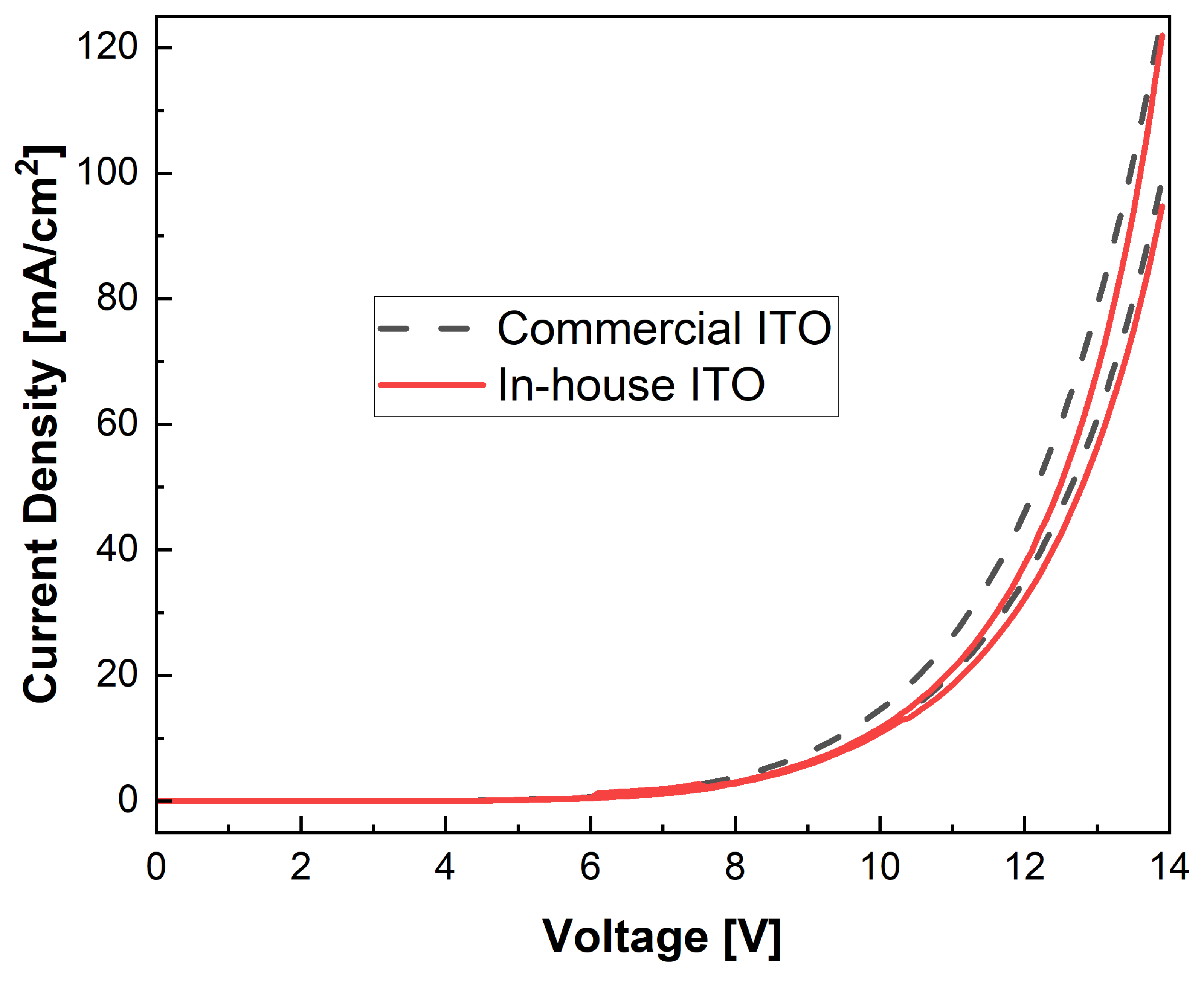
Figure 13 shows the current density vs. voltage curves of the devices made with commercial ITO and in-house ITO. They exhibited similar electrical performance. This suggests that assuming that the materials and interfaces in all the devices behaved the same, the two types of ITO had similar work functions. It is important to underline that the focus of this study was not on optimizing the performance of the OLEDs, thus sub-optimal characteristics are not critical in this regard.

Figure 13.
Comparison of current density vs. voltage characteristics obtained for two of the OLED devices made with commercial ITO anode (dash lines) and two devices made with in-house (solid lines) sputtered ITO anode.
The electroluminescence (EL) analysis was carried out by using a Gooch & Housego OL 770 spectroradiometer (Gooch & Housego (G&H), Ilminster, UK; through Photo Analytical Srl, Settala, Italy) coupled with a G&H OL IS-671-LED Integrating Sphere.
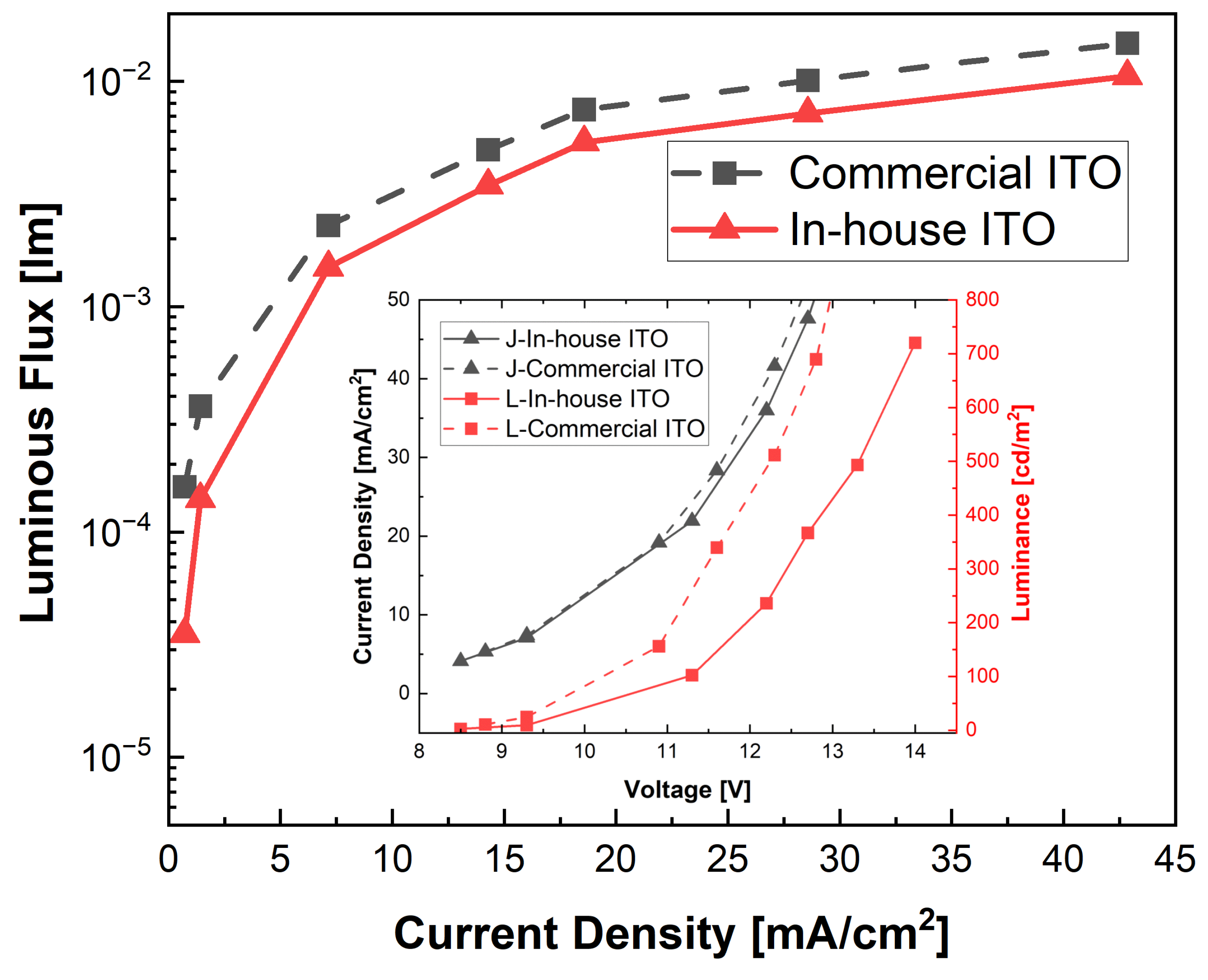
Figure 14 depicts the average measured luminous flux value for each type of device as a function of the current density, while the inset shows a comparison between the current density vs. voltage and luminance vs. voltage of the OLEDs. These optical measurements further confirm that both types of devices achieved comparable performance.
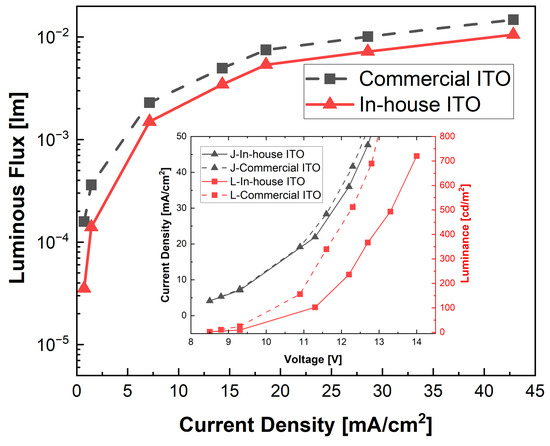
Figure 14.
Luminous flux versus current density of the devices with commercial ITO (dash line) and devices with in-house ITO (solid line). In the inset, the comparison of the JVL plot of OLEDs prepared with commercial (dash lines) and in-house (solid lines) ITO films.
The emission spectra for the two types of devices (shown in Figure 15) exhibited similar peak wavelength (547 nm for the device with commercial ITO and 542 nm for the device with in-house ITO) and comparable bandwidths. The slight difference observed could be attributed to cavity effects generated by small thickness differences in the layers of the device, mainly of the ITO films [60].
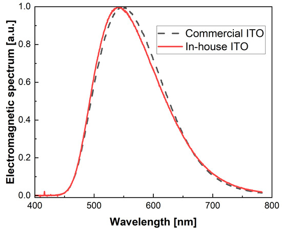
Figure 15.
Comparison of the normalized measured spectra of the OLED devices made with commercial (dash line) and in-house (solid line) sputtered ITO.
4. Conclusions
ITO thin films with properties comparable to commercial ITO were grown on glass substrates by non-reactive RF magnetron sputtering; this means that no oxygen was present in the process chamber during the deposition of the material. Different power densities, argon sputtering pressures, and varying substrate temperatures were tested. The optimal process condition was determined at each step to ensure the best electro-optical performance of the deposited film. The ITO film obtained at a power density of 2.19 W/cm2 and at room temperature showed a maximum transmittance of 82% (at 550 nm) and a resistivity of cm. After fixing the power density, the sputtering pressure was optimized for a room-temperature process. At 6.9 mTorr, the highest growth rate was observed, and the films obtained showed the highest transmittance (about 85%) in the visible region and the minimum resistivity value of cm. Finally, increasing the process temperature was found to have a significant impact on improving the crystallinity of the material, also resulting in a lower sheet resistance of the film. The ITO films prepared at 225 °C, with a power density of 2.19 W/cm2 and a sputtering pressure of 6.9 mTorr, showed a resistivity of Ω cm (corresponding to a conductivity of 4763 S/cm) and a transparency of about 89% in the visible range.
To validate the results obtained, these ITO films were used as the anode for organic light-emitting diodes. These devices were compared to ones made with commercially available ITO (Delta Technologies, Ltd.) on glass substrates. The OLEDs fabricated with the in-house sputtered ITO films exhibited electrical and optical performances that were comparable to those made with commercial ITO substrate. This research suggests that easy steps for optimizing the RF sputtering process, customized for the specific application, can result in high-quality material properties comparable to commercially available alternatives. By eliminating the complex procedure of oxygen incorporation, the complete technique is simplified, making it advantageous for industrial applications that prioritize efficiency, safety, and cost effectiveness.
Author Contributions
Conceptualization, C.D., F.N., and S.A.; Investigation, C.D. and L.M.; Resources, M.G.M. and P.T.; Writing, C.D., F.N., and S.A.; Supervision, C.D., M.G.M., A.R., and P.T. All authors have read and agreed to the published version of the manuscript.
Funding
This research was funded partially by the Italian Ministry of Education, University and Research (MIUR), Public Private Laboratory TRIPODE 2-Progetto RELIGHT (PON02_00556_3306937) (CUP I21J12000040005); partially by the Italian Ministry of Economic Development (MISE), Progetto ISAAC (F/050119/03/X32) (CUP B88I17000590008); partially by the Italian Ministry of Ecological Transition (MITE, now MASE), PTR2022-2024-Progetto 1.5 (CUP I53C22003050001); and partially by ENEA POC202010, Progetto OLEDWIND (CUP I58I20000000005).
Data Availability Statement
Data are available upon request from the authors.
Conflicts of Interest
The authors declare no conflicts of interest.
References
- Chavan, G.T.; Kim, Y.; Khokhar, M.Q.; Hussain, S.Q.; Cho, E.C.; Yi, J.; Ahmad, Z.; Rosaiah, P.; Jeon, C.W. A Brief Review of Transparent Conducting Oxides (TCO): The Influence of Different Deposition Techniques on the Efficiency of Solar Cells. Nanomaterials 2023, 13, 1226. [Google Scholar] [CrossRef]
- Lan, L.; Dai, X.; He, C.; Liu, L.; Yang, X.; Liang, L.; Cao, H.; Peng, J. Improving Negative-Bias-Temperature-Stress Stability for Thin-Film Transistors by Doping Mg Into ScInO Semiconductor. IEEE Trans. Electron Devices 2019, 66, 2620–2623. [Google Scholar] [CrossRef]
- Song, W.; Lan, L.; Xiao, P.; Lin, Z.; Sun, S.; Li, Y.; Song, E.; Gao, P.; Zhang, P.; Wu, W.; et al. High-Mobility and Good-Stability Thin-Film Transistors with Scandium-Substituted Indium Oxide Semiconductors. IEEE Trans. Electron Devices 2016, 63, 4315–4319. [Google Scholar] [CrossRef]
- Liguori, R.; Nunziata, F.; Aprano, S.; Maglione, M.G. Overcoming Challenges in OLED Technology for Lighting Solutions. Electronics 2024, 13, 1299. [Google Scholar] [CrossRef]
- Huseynova, G.; Lee, J.H.; Kim, Y.H.; Lee, J. Transparent Organic Light-Emitting Diodes: Advances, Prospects, and Challenges. Adv. Opt. Mater. 2021, 9, 2002040. [Google Scholar] [CrossRef]
- Liu, L.; Cao, K.; Chen, S.; Huang, W. Toward See-Through Optoelectronics: Transparent Light-Emitting Diodes and Solar Cells. Adv. Opt. Mater. 2020, 8, 2001122. [Google Scholar] [CrossRef]
- Jung, H.S.; Eun, K.; Kim, Y.T.; Lee, E.K.; Choa, S.H. Experimental and numerical investigation of flexibility of ITO electrode for application in flexible electronic devices. Microsyst. Technol. 2017, 23, 1961–1970. [Google Scholar] [CrossRef]
- Ali, M.K.M.; Ibrahim, K.; Pakhuruddin, M.; Faraj, M. Optical and Electrical Properties of Indium Tin Oxide (ITO) Thin Films Prepared by Thermal Evaporation Method on Polyethylene Terephthalate (PET) Substrate. Adv. Mater. Res. 2012, 545, 393–398. [Google Scholar] [CrossRef]
- Kutlimratov, A.; Zufarov, M.A.; Kabulov, R.R.; Xajiyev, M.U. Structial, Electrophysical, and Optical Properties of ITO Films Produced by the Modified CVD Method. Appl. Sol. Energy 2022, 58, 497–502. [Google Scholar] [CrossRef]
- Zuev, D.A.; Lotin, A.A.; Novodvorsky, O.A.; Lebedev, F.V.; Khramova, O.D.; Petuhov, I.A.; Putilin, P.N.; Shatohin, A.N.; Rumyanzeva, M.N.; Gaskov, A.M. Pulsed laser deposition of ITO thin films and their characteristics. Semiconductors 2012, 46, 410–413. [Google Scholar] [CrossRef]
- Hinna, M.; Hartiti, B.; Gouya, A.; Labrim, H.; Fadili, S.; Tahri, M.; Belfhailli, A.; Siadat, M.; Thévenin, P. Synthesis of ITO thin films by Spray pyrolysis based on Taguchi design. Mater Today Proc. 2022, 66, 447–455. [Google Scholar] [CrossRef]
- Wang, K.; Jiao, P.; Cheng, Y.; Xu, H.; Zhu, G.; Zhao, Y.; Jiang, K.; Zhang, X.; Su, Y. ITO films with different preferred orientations prepared by DC magnetron sputtering. Opt. Mater. 2022, 134, 113040. [Google Scholar] [CrossRef]
- Hacini, A.; Ali, A.H.; Adnan, N.N. Optimization of ITO thin film properties as a function of deposition time using the swanepoel method. Opt. Mater. 2021, 120, 111411. [Google Scholar] [CrossRef]
- Zhang, W.; Zhu, G.; Zhi, L.; Yang, H.; Yang, Z.; Yu, A.; Xu, H. Structural, electrical and optical properties of indium tin oxide thin films prepared by RF sputtering using different density ceramic targets. Vacuum 2012, 86, 1045–1047. [Google Scholar] [CrossRef]
- Aydin, E.; Altinkaya, C.; Smirnov, Y.; Yaqin, M.A.; Zanoni, K.P.; Paliwal, A.; Firdaus, Y.; Allen, T.G.; Anthopoulos, T.D.; Bolink, H.J.; et al. Sputtered transparent electrodes for optoelectronic devices: Induced damage and mitigation strategies. Matter 2021, 4, 3549–3584. [Google Scholar] [CrossRef]
- Chauhan, R.N.; Tiwari, N. Preparation of optically transparent and conducting radio-frequency sputtered indium tin oxide ultrathin films. Thin Solid Film. 2021, 717, 138471. [Google Scholar] [CrossRef]
- Daza, L.; Acosta, M.; Castro-RodrÍGUEZ, R.; Iribarren, A. Tuning optical properties of ITO films grown by rf sputtering: Effects of oblique angle deposition and thermal annealing. Trans. Nonferrous Met. Soc. China 2019, 29, 2566–2576. [Google Scholar] [CrossRef]
- Gudmundsson, J.T. Physics and technology of magnetron sputtering discharges. Plasma Sources Sci. Technol. 2020, 29, 113001. [Google Scholar] [CrossRef]
- David, C.; Tinkham, B.; Prunici, P.; Panckow, A. Highly conductive and transparent ITO films deposited at low temperatures by pulsed DC magnetron sputtering from ceramic and metallic rotary targets. Surf. Coatings Technol. 2017, 314, 113–117. [Google Scholar] [CrossRef]
- Kleinhempel, R.; Kaune, G.; Herrmann, M.; Kupfer, H.; Hoyer, W.; Richter, F. Properties of ITO films prepared by reactive magnetron sputtering. Microchim. Acta 2006, 156, 61–67. [Google Scholar] [CrossRef]
- Safi, I. Recent aspects concerning DC reactive magnetron sputtering of thin films: A review. Surf. Coatings Technol. 2000, 127, 203–218. [Google Scholar] [CrossRef]
- Diletto, C.; D’Angelo, A.; Esposito, S.; Guglielmo, A.; Gattia, D.M.; Lanchi, M. Materials Based on Amorphous Al2O3 and Composite W-Al2O3 for Solar Coatings Deposited by High-Rate Sputter Processes. Solar 2023, 3, 113–131. [Google Scholar] [CrossRef]
- Ren, Y.; Liu, P.; Liu, R.; Wang, Y.; Wei, Y.; Jin, L.; Zhao, G. The key of ITO films with high transparency and conductivity: Grain size and surface chemical composition. J. Alloys Compd. 2022, 893, 162304. [Google Scholar] [CrossRef]
- Gwamuri, J.; Marikkannan, M.; Mayandi, J.; Bowen, P.; Pearce, J. Influence of Oxygen Concentration on the Performance of Ultra-Thin RF Magnetron Sputter Deposited Indium Tin Oxide Films as a Top Electrode for Photovoltaic Devices. Materials 2016, 9, 63. [Google Scholar] [CrossRef] [PubMed]
- Najwa, S.; Shuhaimi, A.; Talik, N.; Ameera, N.; Sobri, M.; Rusop, M. In-situ tuning of Sn doped In2O3 (ITO) films properties by controlling deposition Argon/Oxygen flow. Appl. Surf. Sci. 2019, 479, 1220–1225. [Google Scholar] [CrossRef]
- Miao, J.; Fan, T. Flexible and stretchable transparent conductive graphene-based electrodes for emerging wearable electronics. Carbon 2023, 202, 495–527. [Google Scholar] [CrossRef]
- Pode, R. Organic light emitting diode devices: An energy efficient solid state lighting for applications. Renew. Sustain. Energy Rev. 2020, 133, 110043. [Google Scholar] [CrossRef]
- Hong, G.; Gan, X.; Leonhardt, C.; Zhang, Z.; Seibert, J.; Busch, J.M.; Bräse, S. A Brief History of OLEDs—Emitter Development and Industry Milestones. Adv. Mater. 2021, 33, 2005630. [Google Scholar] [CrossRef]
- Negi, S.; Mittal, P.; Kumar, B. Impact of different layers on performance of OLED. Microsyst. Technol. 2018, 24, 4981–4989. [Google Scholar] [CrossRef]
- Liu, S.; Xie, W.; Lee, C.S. Organic light-emitting diodes, what’s next? Next Nanotechnol. 2023, 1, 100003. [Google Scholar] [CrossRef]
- Tang, C.W.; Van Slyke, S.A. Organic electroluminescent diodes. Appl. Phys. Lett. 1987, 51, 913–915. [Google Scholar] [CrossRef]
- Chuang, M. ITO Films Prepared by Long-throw Magnetron Sputtering without Oxygen Partial Pressure. J. Mater. Sci. Technol. 2010, 26, 577–583. [Google Scholar] [CrossRef]
- Saenko, A.V.; Vakulov, Z.E.; Klimin, V.S.; Bilyk, G.E.; Malyukov, S.P. Effect of Magnetron Sputtering Power on ITO Film Deposition at Room Temperature. Russ. Microelectron. 2023, 52, 297–302. [Google Scholar] [CrossRef]
- Kudryashov, D.; Gudovskikh, A.; Zelentsov, K. Low temperature growth of ITO transparent conductive oxide layers in oxygen-free environment by RF magnetron sputtering. J. Phys. Conf. Ser. 2013, 461, 012021. [Google Scholar] [CrossRef]
- Tchenka, A.; Agdad, A.; Vall, M.C.S.; Hnawi, S.K.; Narjis, A.; Nkhaili, L.; Ibnouelghazi, E.; Ech-Chamikh, E. Effect of RF Sputtering Power and Deposition Time on Optical and Electrical Properties of Indium Tin Oxide Thin Film. Adv. Mater. Sci. Eng. 2021, 2021, 556305. [Google Scholar] [CrossRef]
- Asri, R.; Hamzah, N.; Ahmad, M.; Taib, M.M.; Sahil, S.; Hassan, Z. Role of RF Magnetron Sputtering Power on Optical and Electrical Properties of ITO Films on Soda-Lime Glass Substrates. J. Phys. Conf. Ser. 2020, 1535, 012035. [Google Scholar] [CrossRef]
- Schiller, S.; Heisig, U.; Goedicke, K. Use of the ring gap plasmatron for high rate sputtering. Thin Solid Films 1977, 40, 327–334. [Google Scholar] [CrossRef]
- Robb, A.J.; Duca, Z.A.; White, N.; Woodell, P.; Ward, P.A. Influence of oxygen on the optical and electrical properties of magnetron-sputtered indium tin oxide thin films at ambient temperature. Thin Solid Films 2024, 788, 140152. [Google Scholar] [CrossRef]
- Yasrebi, N.; Bagheri, B.; Yazdanfar, P.; Rashidian, B.; Sasanpour, P. Optimization of Sputtering Parameters for the Deposition of Low Resistivity Indium Tin Oxide Thin Films. Acta Metall. Sin. Engl. Lett. 2014, 27, 324–330. [Google Scholar] [CrossRef]
- Sousa, M.; da Cunha, A. Optimization of low temperature RF-magnetron sputtering of indium tin oxide films for solar cell applications. Appl. Surf. Sci. 2019, 484, 257–264. [Google Scholar] [CrossRef]
- Li, J.; Jiang, L.; Li, X.; Luo, J.; Liu, J.; Wang, M.; Yan, Y. Different Crystallization Behavior of Amorphous ITO Film by Rapid Infrared Annealing and Conventional Furnace Annealing Technology. Materials 2023, 16, 3803. [Google Scholar] [CrossRef] [PubMed]
- Nasir, M.F.B.M.; Mamat, M.H. Effect of substrates temperature on structural and optical properties indium tin oxide prepared by RF magnetron sputtering. In Proceedings of the 2016 IEEE Student Conference on Research and Development (SCOReD), Kuala Lumpur, Malaysia, 13–14 December 2016; pp. 1–4. [Google Scholar] [CrossRef]
- Chen, Y.; Zhou, Y.; Zhang, Q.; Zhu, M.; Liu, F. The correlation between preferred orientation and performance of ITO thin films. J. Mater. Sci. Mater. Electron. 2007, 18, 411–414. [Google Scholar] [CrossRef]
- Shigeno, E.; Shimizu, K.; Seki, S.; Ogawa, M.; Shida, A.; Ide, M.; Sawada, Y. Formation of indium-tin-oxide films by dip coating process using indium dipropionate monohydroxide. Thin Solid Films 2002, 411, 56–59. [Google Scholar] [CrossRef]
- Cruz, L.; Legnani, C.; Matoso, I.; Ferreira, C.; Moutinho, H. Influence of pressure and annealing on the microstructural and electro-optical properties of RF magnetron sputtered ITO thin films. Mater. Res. Bull. 2004, 39, 993–1003. [Google Scholar] [CrossRef]
- Shigesato, Y.; Hayashi, Y.; Haranoh, T. Doping mechanisms of tin-doped indium oxide films. Appl. Phys. Lett. 1992, 61, 73–75. [Google Scholar] [CrossRef]
- Amanullah, F.; Pratap, K.; Babu, V.H. Characterization of isochronally and isothermally annealed indium tin oxide thin films. Thin Solid Films 1995, 254, 28–32. [Google Scholar] [CrossRef]
- Kobayashi, H.; Ishida, T.; Nakamura, K.; Nakato, Y.; Tsubomura, H. Properties of indium tin oxide films prepared by the electron beam evaporation method in relation to characteristics of indium tin oxide/silicon oxide/silicon junction solar cells. J. Appl. Phys. 1992, 72, 5288–5293. [Google Scholar] [CrossRef]
- Qiao, Z.; Mergel, D. Comparison of radio-frequency and direct-current magnetron sputtered thin In2O3:Sn films. Thin Solid Films 2005, 484, 146–153. [Google Scholar] [CrossRef]
- Kumar, C.V.R.V.; Mansingh, A. Effect of target-substrate distance on the growth and properties of rf-sputtered indium tin oxide films. J. Appl. Phys. 1989, 65, 1270–1280. [Google Scholar] [CrossRef]
- Kim, J.; Shrestha, S.; Souri, M.; Connell, J.G.; Park, S.; Seo, A. High-temperature optical properties of indium tin oxide thin-films. Sci. Rep. 2020, 10, 12486. [Google Scholar] [CrossRef]
- Tuna, O.; Selamet, Y.; Aygun, G.; Ozyuzer, L. High quality ITO thin films grown by dc and RF sputtering without oxygen. J. Phys. D Appl. Phys. 2010, 43, 055402. [Google Scholar] [CrossRef]
- Nunziata, F.; Aprano, S.; Liguori, R.; Maglione, M.G.; Tassini, P.; Rubino, A. ITO sputtering study for transparent OLED top electrode. In Organic Electronics and Photonics: Fundamentals and Devices IV; Reineke, S., Vandewal, K., Maes, W., Eds.; SPIE: Bellingham, WA, USA, 2024; Volume 6, p. 2. [Google Scholar] [CrossRef]
- Chao, Y.; Tang, W.; Wang, X. Properties of Resistivity, Reflection and Absorption Related to Structure of ITO Films. J. Mater. Sci. Technol. 2012, 28, 325–328. [Google Scholar] [CrossRef]
- Wohlmuth, W.; Adesida, I. Properties of R.F. magnetron sputtered cadmium–tin–oxide and indium–tin–oxide thin films. Thin Solid Films 2005, 479, 223–231. [Google Scholar] [CrossRef]
- Reddy, V.S.; Das, K.; Dhar, A.; Ray, S.K. The effect of substrate temperature on the properties of ITO thin films for OLED applications. Semicond. Sci. Technol. 2006, 21, 1747–1752. [Google Scholar] [CrossRef]
- Dong, B.; Yan, J.; Li, G.; Xu, Y.; Zhao, B.; Chen, L.; Wang, H.; Li, W. High luminance/efficiency monochrome and white organic light emitting diodes based pure exciplex emission. Org. Electron. 2022, 106, 106528. [Google Scholar] [CrossRef]
- Sheng, R.; Yang, L.; Li, A.; Chen, K.; Zhang, F.; Duan, Y.; Zhao, Y.; Chen, P. Highly efficient orange and white OLEDs based on ultrathin phosphorescent emitters with double reverse intersystem crossing system. J. Lumin. 2022, 246, 118852. [Google Scholar] [CrossRef]
- Li, X.; Liu, W.; Zhu, Q.; Wu, R.; Liu, G.; Zhou, L. High-performance full phosphorescent warm white organic light-emitting diodes with external quantum efficiency of 34.5%. Opt. Mater. 2022, 124, 112005. [Google Scholar] [CrossRef]
- Li, X.; Liu, W.; Chen, K.; Yu, C.; Xia, X.; Liu, G.; Zhou, L. Very bright and efficient ITO-free narrow-spectrum micro-cavity top-emitting organic light-emitting diodes with low operation voltage. J. Mater. Chem. C 2022, 10, 3241–3247. [Google Scholar] [CrossRef]


Disclaimer/Publisher’s Note: The statements, opinions and data contained in all publications are solely those of the individual author(s) and contributor(s) and not of MDPI and/or the editor(s). MDPI and/or the editor(s) disclaim responsibility for any injury to people or property resulting from any ideas, methods, instructions or products referred to in the content. |
© 2024 by the authors. Licensee MDPI, Basel, Switzerland. This article is an open access article distributed under the terms and conditions of the Creative Commons Attribution (CC BY) license (https://creativecommons.org/licenses/by/4.0/).