Article

Influence of the Acetylene Flow Rate and Process Pressure on the Carbon Deposition Behavior by Thermal Chemical Vapor Deposition Process

1
Heat & Surface Technology R&D Group, Korea Institute of Industrial Technology, Siheung 15014, Republic of Korea
2
Department of Materials Science and Engineering, Yonsei University, Seoul 03722, Republic of Korea
*
Authors to whom correspondence should be addressed.
Crystals 2024, 14(9), 782; https://doi.org/10.3390/cryst14090782
Submission received: 29 July 2024 / Revised: 18 August 2024 / Accepted: 20 August 2024 / Published: 31 August 2024
(This article belongs to the Section Crystal Engineering)

Abstract

:
We used the chemical vapor deposition process to deposit carbon film at a high temperature (900 °C). The carbon films were deposited on AISI 1006 foils using an acetylene gas. We analyzed the carbon film deposited on the surface using Raman spectroscopy, scanning electron microscopy, and high-resolution transmission electron microscopy to define changes in the bonding structure of the carbon film. The results of Raman spectroscopy and high-resolution transmission electron microscopy revealed that as the acetylene flow rate increased, the shape of the deposited carbon film changed from graphene to graphite. In addition, in order to compare the quality of the carbon film in terms of mechanical and electrical properties, carbon films treated under various conditions were closely analyzed using nano-indenter and a sheet resistance meter. Therefore, the optimal condition (1 Torr-50 sccm) was selected in which graphene was uniformly deposited and had the lowest electrical resistance (500 Ω/sq) and highest hardness (12 GPa).

1. Introduction

Graphene has carbon atoms forming an sp2 bond and has a 2D hexagonal structure with a thickness of one atomic layer [1,2,3]. The carbon layer formed by graphene has excellent physical properties such as high chemical stability, electron mobility, quantum hall effect, and electrical conductivity; therefore, it can be used in transistors, sensors, actuators, flexible and transparent conducting films, etc. [4,5]. However, since complex shapes and large surface areas are required for synthesis to these functional parts, large-scale graphene application technology must be developed. To synthesize graphene, research has been conducted on various methods such as mechanical exfoliation, wet chemical synthesis, arc discharge, and CVD (chemical vapor deposition) [6,7,8,9,10,11,12]. Graphene produced by physical methods is very limited in terms of commercialization due to its small size and limited yield. On the other hand, the CVD process is economical with regard to process cost and allows for uniform and high-quality graphene growth on a large scale by adsorbing carbon well on the surface of the catalyst metal at high temperature. In 2008, there was a study that grew graphene on transition metal Ni and Cu substrates by injecting methane gas through CVD for the first time, and related research activities have increased explosively since then [13,14]. One of the keys to growing graphene is to select an appropriate hydrocarbon and deposit the decomposed carbon near the surface of the transition metal substrate. The transition metal used as a substrate not only plays a catalytic role in lowering the reaction energy barrier, but also determines the graphene growth mechanism. As shown in Table 1, transition metals such as copper (Cu), nickel (Ni), cobalt (Co), platinum (Pd), iron (Fe), and germanium (Ge) are used as substrates, and the carbon solubility limit and graphene formation mechanism are different depending on the type.
Iron, one of the transition metals, is a very useful material because it is cheap and easy to access. In contrast to other transition metals, iron is used to increase strength in the carburizing process. In recent research, several studies have been conducted on forming graphene on an iron substrate during the carburizing process [24,25]. Graphene formed on the iron surface or grain boundaries not only provides superior mechanical and electrical properties at the outermost surface compared to conventional carburization, but also provides high corrosion resistance and durability to the iron surface with high chemical safety. Theoretically, it is feasible to form graphene on the iron surface. This is because, at room temperature, the lattice constant of iron (2.86 A) is close to that of graphene (2.46 A) [26]. Iron has allotropes such as ferrite phase and austenite phase depending on the heating temperature, and the carbon solubility limit is 0.022 wt.% and 1.43 wt.%, respectively. Therefore, it is necessary to employ carbon at a temperature (above 730 °C) where austenite exists, and then to force outward diffusion of the carbon employed on the surface through continuous cooling at a temperature that transforms into ferrite (less than 730 °C). Figure 1 shows the mechanism by which carbon is applied to the iron (Fe) surface according to the CVD process. After heating to the target treatment temperature, Ar and H2 gases are injected to activate the surface so that the carbon can easily penetrate. Acetylene is supplied into the furnace to deposit carbon, and the carbon isotrope formed in this part is determined. Since acetylene molecules have a triple bond, it is difficult for them to thermally decompose on their own; therefore, they diffuse to the steel surface using iron as a catalyst. While there is a mechanism by which a graphene layer is applied through the cooling process, if a relatively high-pressure acetylene is injected in the atmosphere, polycyclic aromatic hydrocarbons (PAHs) are formed by their own thermal decomposition, making it easy for graphite to form in a form similar to soot.
Since the decomposition temperature and speed of supplying carbon to the base material are different depending on the type of carbon source, the energy barrier for forming graphene is different. Hydrocarbon gases used to form CVD graphene are mainly methane (CH4), ethane (C2H6), acetylene (C2H2), and ethylene (C2H4). Methane requires a high activation energy of about 410 kJ mol−1 to adsorb carbon to the substrate; therefore, a high flow rate and high temperature atmosphere are required as a carbon source [27]. Sun et al. [28] grew graphene on Cu foil using ethylene, which has a lower binding energy (368 kJ mol−1) than methane, at a temperature of 750 °C, and the graphene growth time was 420 μm min−1. Chen et al. [29] studied growing graphene on an Ni substrate according to the acetylene flow rate using acetylene as a carbon source. Although acetylene has a high binding energy (965 kJ mol−1), it has a fast decomposition rate due to the catalyst metal; therefore, carbon can be easily deposited. However, excessive carbon supply may result in the formation of graphite with high defect density. In other words, by deriving process conditions through several experiments, it is possible to control the form of carbon deposited on the surface of the substrate and the resulting properties. Although several studies have been conducted to grow graphene on iron substrates, there have been few studies that closely observed the extent to which carbon films are deposited to the iron surface and bonding structure of carbon atoms depending on carburizing conditions. Additionally, there have been few studies on finding application conditions that satisfy mechanical and electrical properties while using minimal gas. The main objective of this study is to optimize the carbon coating conditions to minimize the electrical resistance and obtain excellent mechanical properties by using appropriate acetylene. Therefore, by examining the change in carbon layer coating under various acetylene flow rates and pressure conditions, the optimal carbon coating conditions for obtaining specific properties can be selected.

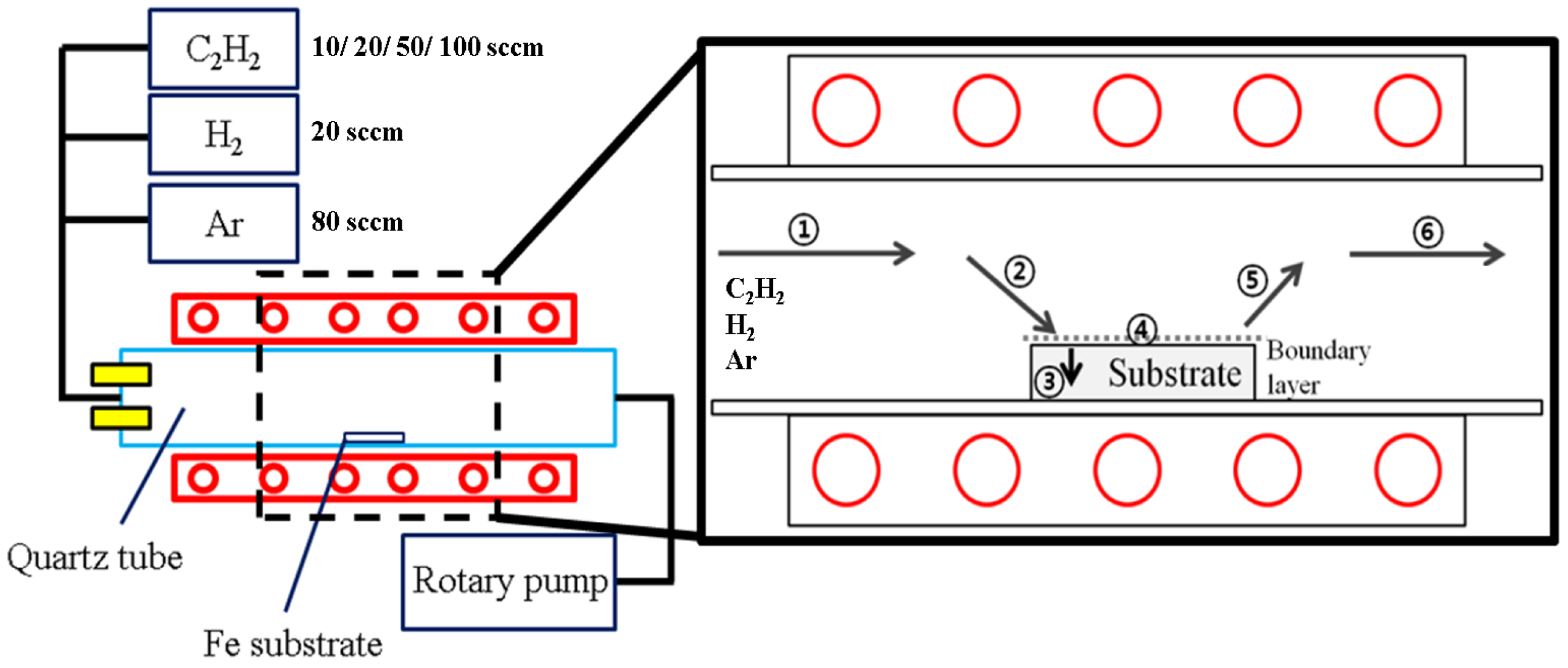
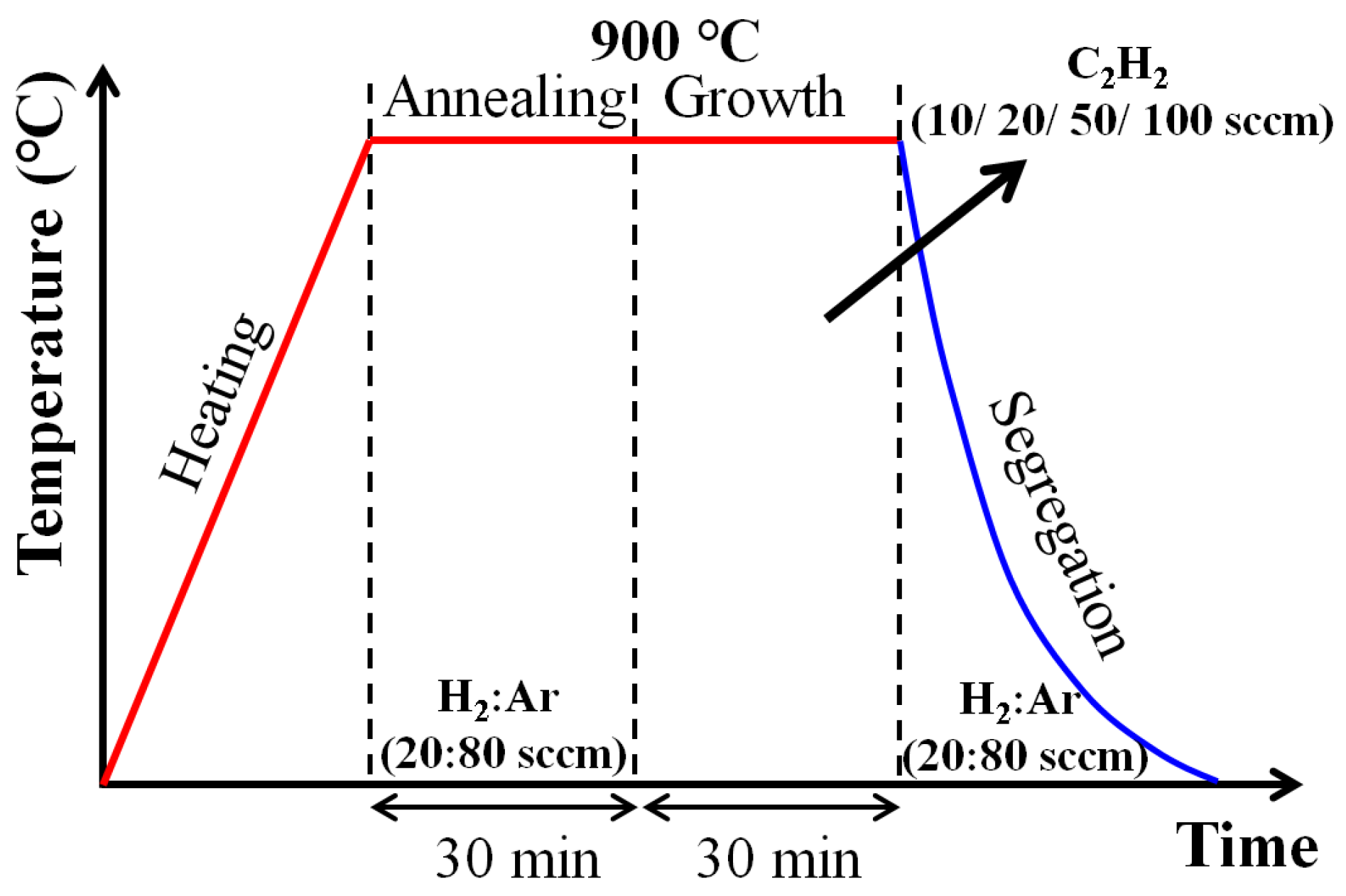
2. Experimental Method

2.1. Graphene Synthesis

In this study, the carbon layer was applied by chemical vapor deposition using a quartz tube-structured thermal CVD equipment with a hot zone area of 100 mm in diameter and 250 mm in length, as shown in Figure 2. The CVD equipment used can be electrically heated up to 1100 °C, and the hot zone is made of quartz with excellent heat and chemical resistance. The AISI 1006 steel (30 mm Ø × 100 μm h, see Table 2) in the shape of a foil used as a catalyst metal was surface-polished using SiC paper and alumina suspension, and the average surface roughness of the specimen was set to 0.02 μm as the initial condition. Foil specimen was fixed at the center of the hot zone, and then graphene growth was performed using a four-step process schedule as shown in Figure 3.
The detailed process schedule for graphene growth is shown in Figure 3. Step 1 is heating to the reaction temperature, using a turbopump to maintain a high vacuum atmosphere (0.000003 Torr) and heating from 12.8 °C/s to 900 °C. Step 2 is an annealing step in which H2 and Ar are injected at 20 and 80 sccm, respectively, while maintaining the heating temperature, in which the oxide layer and residual contaminant on the iron foil surface are removed and the grain boundary of the surface is increased to facilitate graphene formation. In Step 3, after the heat treatment was completed, acetylene gas was injected as the main growth stage, and synthesis was performed for 30 min. At this stage, acetylene is decomposed and penetrates and diffuses on the surface of substrate. Step 4 is the cooling step, the last step in graphene synthesis. H2 and Ar were introduced at flow rates of 20 sccm and 80 sccm, respectively, and the heater cover was opened to quickly cool to room temperature at a rate of about 24.5 °C/s.

2.2. Graphene Characterization

An optical microscope was used to macroscopically observe the degree of application of the graphene film formed on the iron foil, and Raman spectroscopy (Horiba JY, Japan, Kyoto, LabRam HR evolution) was used to closely analyze the bonding structure of the applied carbon. An Ar laser with a length of 514 nm was irradiated on the surface of the specimen. To observe the carbon shape, the surface of the specimen was analyzed at magnifications of ×4000 and ×20,000 using scanning electron microscopy (FEI Hong Kong Company, China, Hong Kong, NNS 450). To measure the hardness of the surface of the treated specimen, a nano indenter (Fischer Instruments, Japan, Saitama, HM 2000) and a Vickers hardness meter (Mitutoyo, Japan, Kanagawa, HB-210B) were indented with loads of 1 mN and 10 gf, respectively. To analyze the electrical properties of the applied graphene, sheet resistance was measured using a sheet resistance meter (AIT, South Korea, Suwon, CMT-SR2000N) in a four-point system. A probe capable of applying current was contacted at two points on the outside of the specimen, and a probe capable of measuring voltage was contacted at two points on the inside of the specimen. The diameter and thickness of the specimen were 30 mm and 0.1 mm, respectively, and the spacing between the probes was set to 4.5 mm. Since the ratio of thickness to probe spacing is 2.5%, the correlation factor was calculated as 0.999. The measurement method measures current and voltage with a probe configured at regular intervals, then substitutes correction coefficients related to specimen size, thickness, and measurement temperature into Equation (1) to measure sheet resistance. Rs, V, I, C.F. mean sheet resistance [Ω/sq], voltage [V], current [A], and correction factor, respectively.
R s = V I × C . F .
Carbon film was synthesized by partially changing the process parameter under existing vacuum carburizing conditions that use acetylene gas as a carbon source to increase the mechanical properties of low alloy steel, and acetylene flow rates (10, 20, 50, 100 sccm) and process pressure (1, 10 Torr) were set as a variable and an experiment was conducted to find process conditions that provide excellent mechanical and electrical properties to the product surface.

3. Results and Discussion

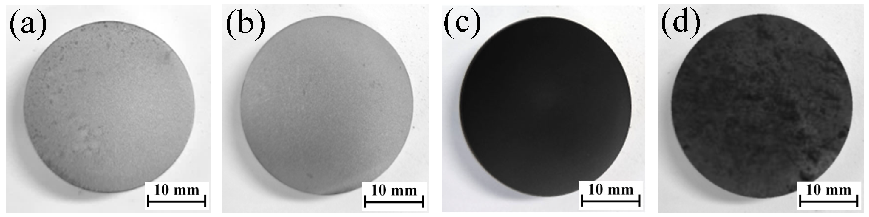
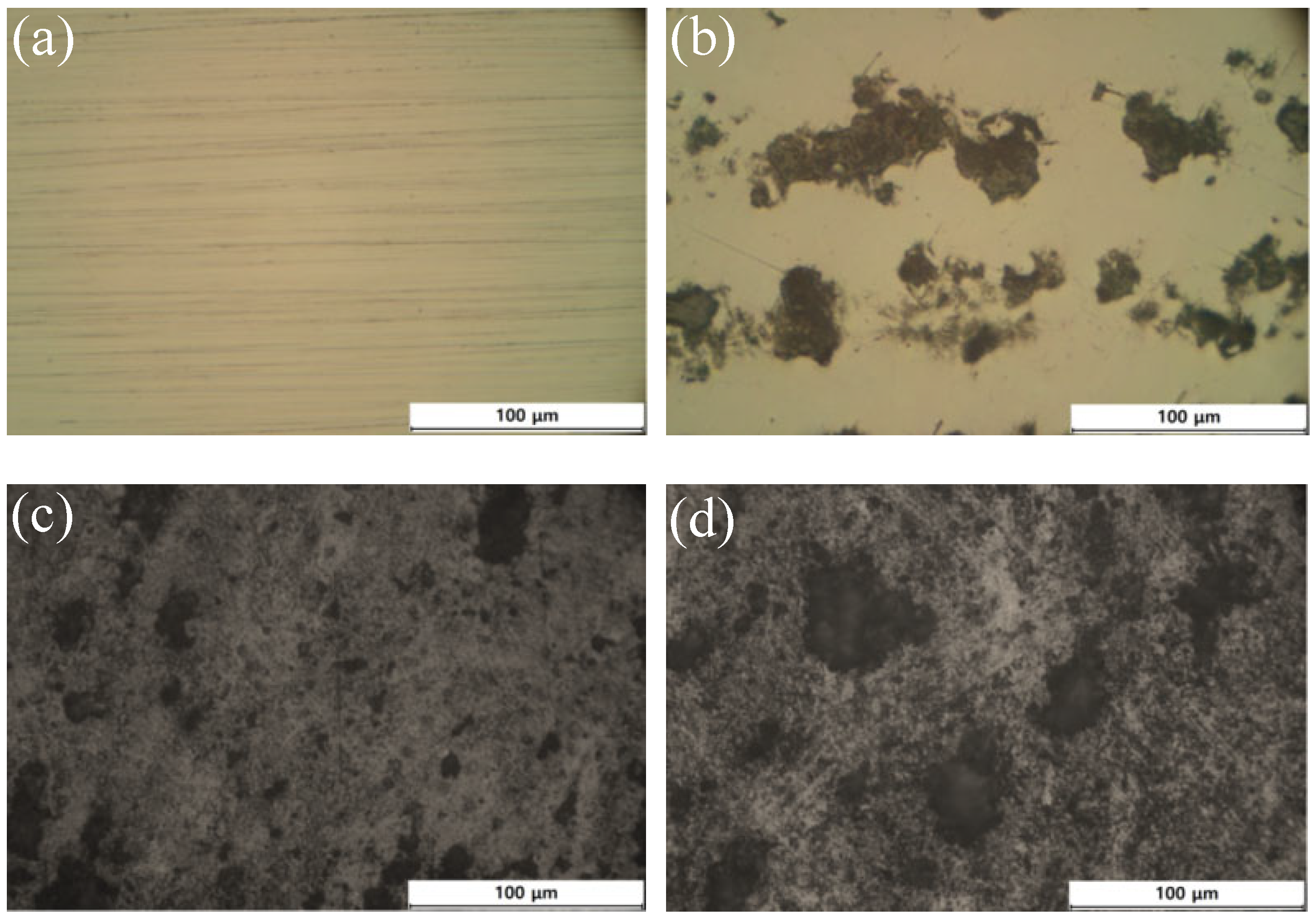
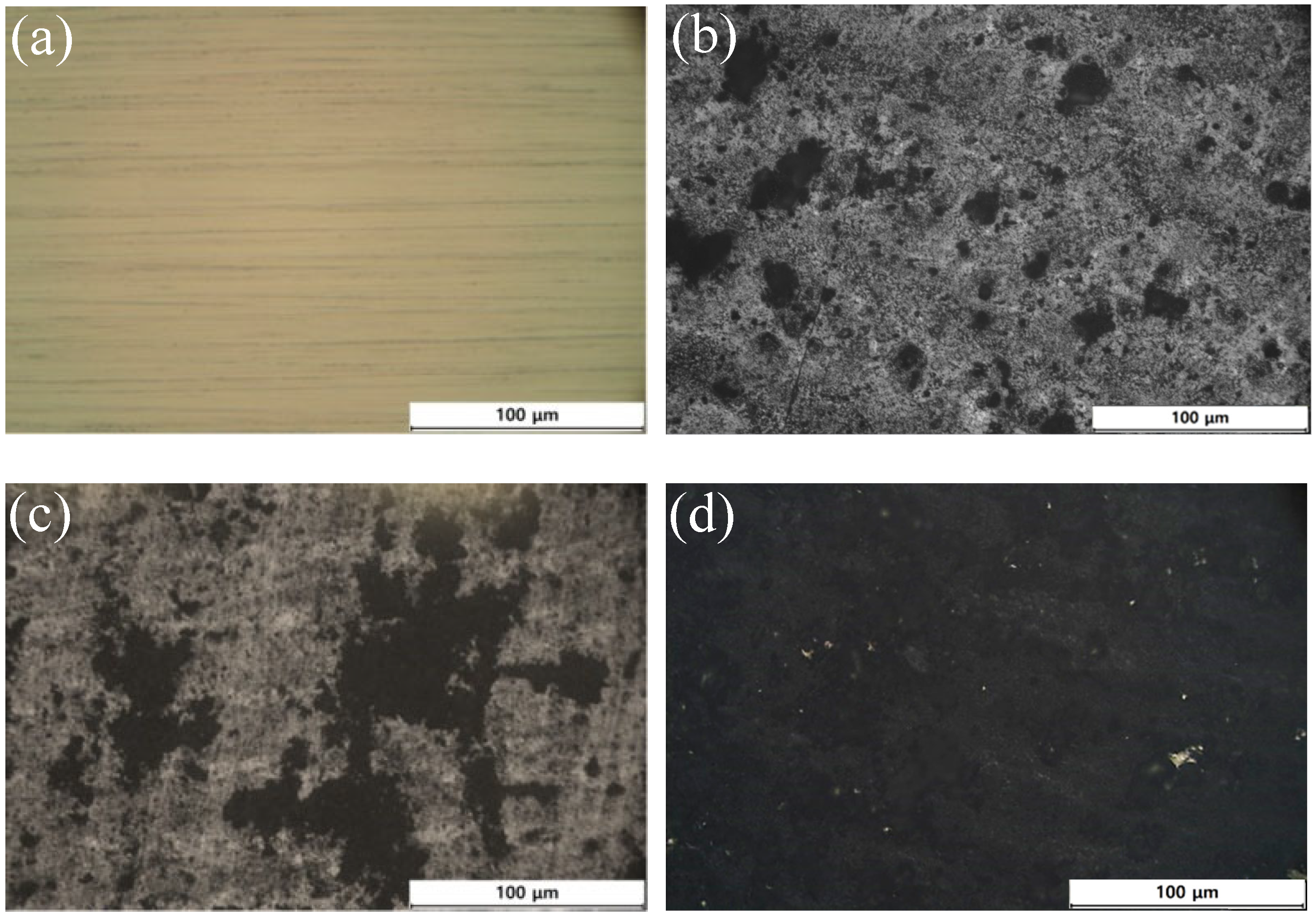
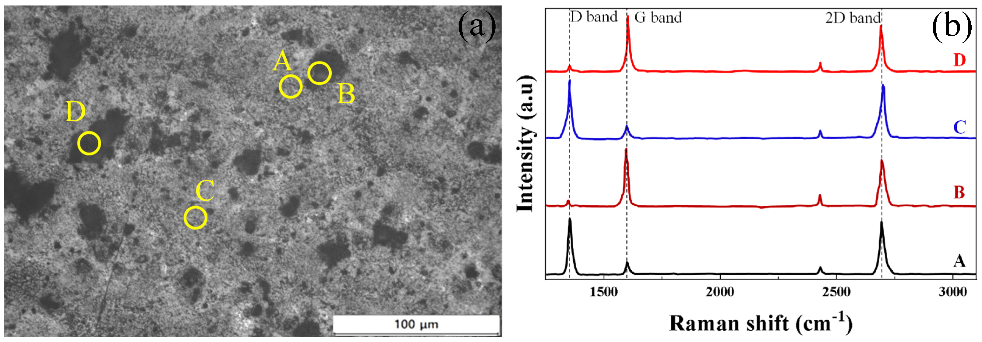
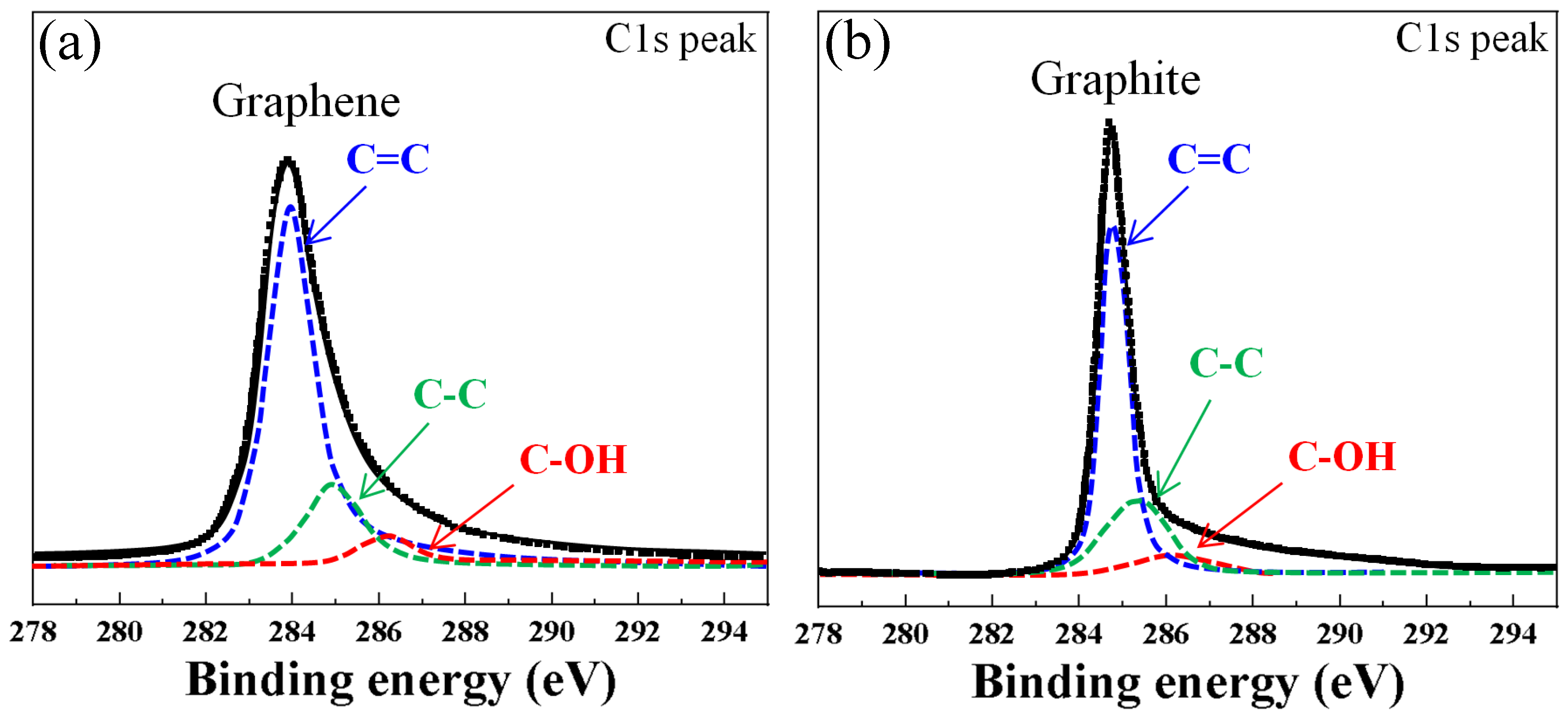
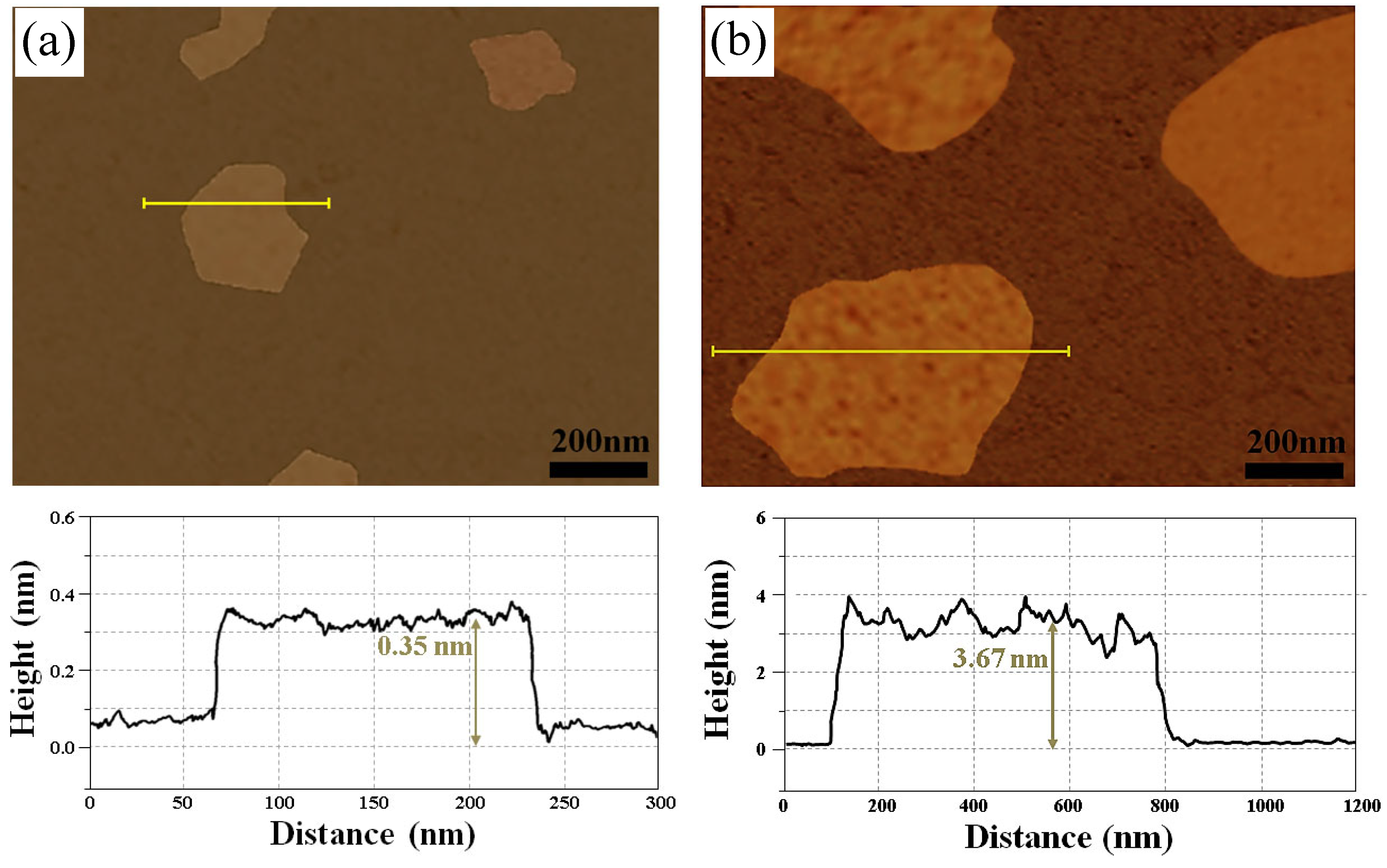
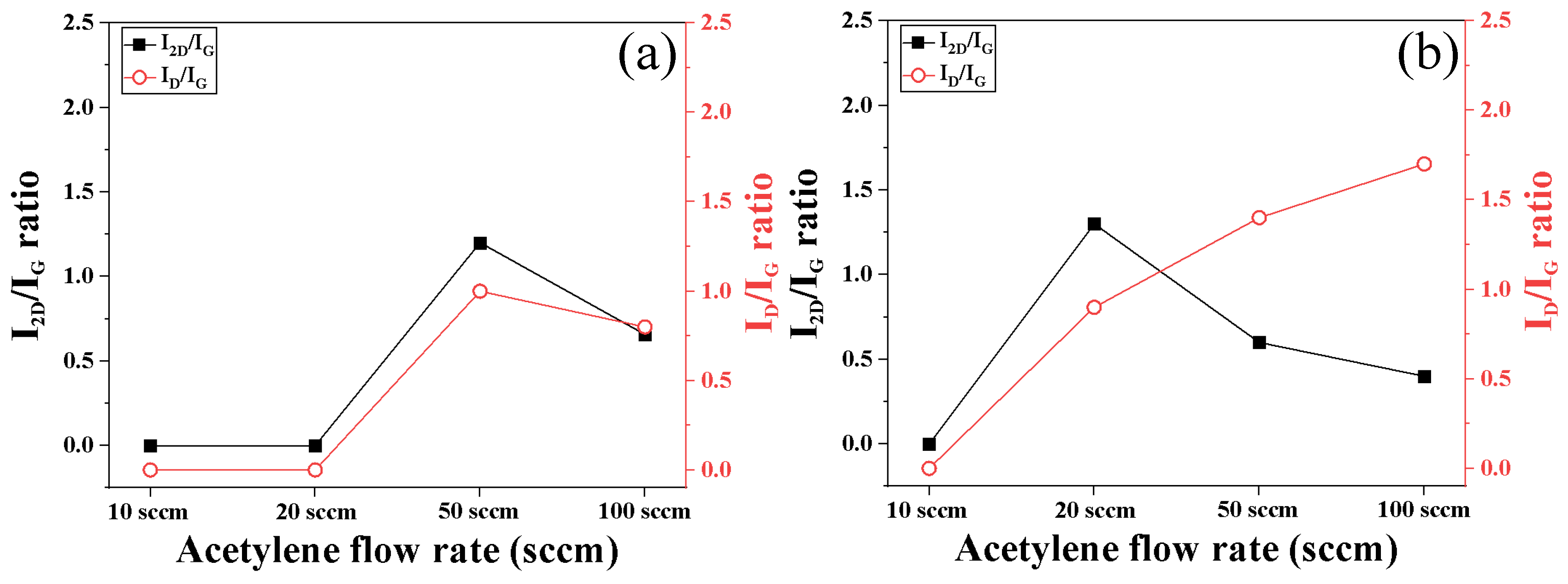
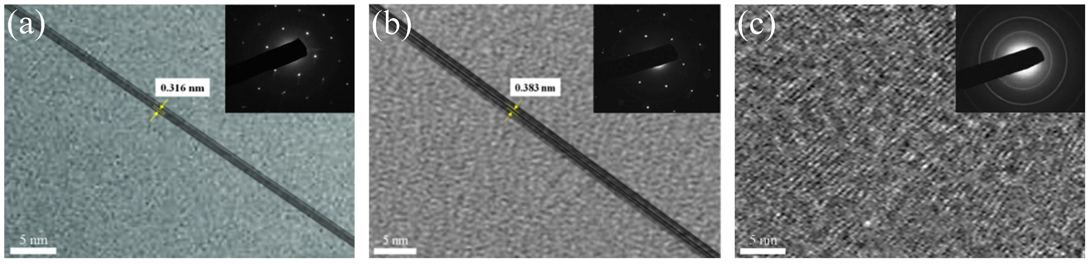
3.1. Surface Morphology

Figure 4 is a photograph of the surface of a specimen treated according to the acetylene flow rate at 10 torr. The surface color according to the acetylene flow rate is light gray, similar to the color of the carburized specimen in the specimen under 10 and 20 sccm conditions. However, under the condition of 50 sccm, the surface color is relatively dark midnight gray and the surface is smooth and clean. On the other hand, the surface color under the 100 sccm condition is black, and black particles can be seen around the surface. Due the fact that the amount of carbon that has penetrated into the surface is small under low flow rates (10 and 20 sccm), there is little change in color on the surface of the specimen. However, at the maximum flow rate condition (100 sccm), it was determined that pyrolyzed carbon had formed on the specimen surface due to the high carbon flux supply and the high-density pure acetylene atmosphere. The reason why the surface color changes depending on the acetylene flow rate is because the amount of carbon diffusion during the growth stage and the behavior of carbon deposition during the segregation stage are different.
As shown in Figure 5, the microstructure of carbon deposited to the substrate according to the acetylene flow rate at 1 Torr process pressure was observed using an optical microscope. The difference in surface optical contrast is clearly observed depending on the acetylene flow conditions. Carbon was not observed on the surface of the specimen under the 10 sccm condition, and as the flow rate increases from 20 sccm, the area of dark gray carbon deposition increases. Under the 50 sccm condition, the overall surface exhibits a dark gray color. As the flow rate increases, the proportion of the surface area that appears black also increases.
As shown in Figure 6, the microstructure of carbon deposited to the substrate according to the acetylene flow rate at 10 Torr process pressure was observed using an optical microscope. Under 20 sccm conditions, the specimen surface mostly has a dark gray area, with some black particles. In particular, as the flow rate increases, the area with black color increases, and most of the surface under the 100 sccm treatment condition was deposited with a black color layer, which is expected to be a carbon film.
To identify the bonding structure of the carbon layer applied to the surface of the specimen under the conditions of 10 torr and 20 sccm, Raman analysis was performed by selecting four locations (A, B, C, D) where carbon was applied, as shown in Figure 7. Peaks commonly detected at all locations are broadly divided into two types: G band (1580 cm−1) and 2D band (2700 cm−1). G band and 2D band are formed by E2g vibrational mode and second-order two phonon mode, respectively [30]. The D band (1350 cm−1) is not measured in defect-free graphene, but is easily observed in graphene whose symmetry is broken due to structural defects [31]. The A, C locations have a dark gray color, and the intensity of the 2D peak is higher than that of the G peak; therefore, they are judged to be a single layer graphene. The B, C locations have a black color, and are judged to be graphite because the 2D peak and G peak are almost similar [32].
Using Raman analysis, different carbon coating layers (graphite, graphene) were distinguished by color at each location and compared through their chemical bonding structures. Figure 8 shows the C1s spectra analyzed by XPS for the dark gray and black areas. In the C1s spectra, the C=C bond and C-C bond were detected at 284.5 eV and 285.3 eV, respectively, and the C-OH bond was detected at 286.6 eV. The area of the C-C bond generated by sp3 bonding is smaller in the black area, which is assumed to be graphite, than in the dark gray area. In particular, graphene with the dark gray area has a higher C-OH bond than graphite. It is inferred that the peaks of these bonds increase due to the segregation reaction from the dissolved carbon, not due to carbon coating by pyrolysis.
AFM equipment was used to measure the lateral size and thickness of carbon layers with different optical properties observed in Figure 7. Figure 9 shows some representative AFM images with height profiles of the lines being shown on the bottom of each image. Figure 9a is an AFM image measuring the dark gray area, and the lateral size and thickness of the carbon layer were measured as 175 nm and 0.35 nm, respectively. As a result of external factors such as AFM equipment and substrate, the dark gray area is considered to be monolayer graphene, as multilayer graphene is usually measured as 0.5 and 1 nm by AFM equipment. Figure 9b shows a wide scan image of a carbon flake with a black color, and the lateral size and thickness of the carbon layer were measured to be 700 nm and 3.67 nm, respectively. Since the pyrolytic carbon formed on the surface of the specimen by pyrolysis has a size of 2–15 μm, the carbon layer is considered to be graphite.
Figure 10 is a microstructure photograph observed at high magnification using SEM equipment to analyze the shape of the carbon deposited in the two locations (A, B) specified in Figure 7. Figure 10a is the boundary where both A and B areas exist. On the left side of the microscope (A), it is observed into graphene layer with relatively flat carbon deposited on the surface, and the right side (B) is divided into graphite layer with carbon irregularly deposited in the form of particles. The average width of the graphene layer formed in the form of a sheet is about 124~167 nm, and a detailed analysis of the thickness will be explained through TEM analysis. The particle size of graphite formed in bulk is approximately from 0.6 to 1.2 μm, which is considered to be fine graphite.
Figure 11 shows the results showing the change in Raman spectra intensity ratio according to process pressure and acetylene flow rate. The relative peak ratio of the G band and the 2D band is related to the number of graphene coating layers [33,34]. The smaller the ratio between the G peak and the 2D peak (I2D/IG), the more likely it is to have a turbostratic structure with a graphitic structure or graphene with a multilayer structure [35]. On the other hand, as I2D/IG increases, single-layer graphene, which is frequently observed in physical vapor deposition, can be observed [36]. In the case of 1 Torr condition in Figure 11a, the Raman peak was not measured until 20 sccm, but the Raman peak due to the carbon film layer was observed from 50 sccm. As the acetylene flow rate increases, I2D/IG tends to decrease and the carbon structure changes from a single-layer graphene structure to a multi-layer graphene structure. As the acetylene flow rate increases, the ID/IG ratio decreases; therefore, it is easy to form a carbon structure with low defect density and high crystallinity. In particular, the carbon structure can vary depending on the pressure difference, and in the case of 10 Torr conditions, the I2D/IG ratio is about 30% lower than 1 Torr. This is because the acetylene density inside the furnace increases due to high pressure; therefore, multilayer graphene or graphite is likely to be formed under the same flow rate conditions. Additionally, as the acetylene flow rate increases, the ID/IG ratio increases, resulting in lower crystallinity and the formation of a low-quality carbon structure.
Figure 12 shows the TEM image and Selected Area Electron Diffraction (SAED) pattern results analyzed using HRTEM on the surface of the specimen treated according to the acetylene flow rate. HRTEM images are data that can directly confirm the quality of graphene, such as the number of carbon layers deposited on the surface of the specimen and bonding structure. The carbon structure formed at a relatively low acetylene flow rate (20 sccm) is few layer graphene (FLG), which has approximately four layers with an interlayer spacing of about 0.316 nm (Figure 12a). When the acetylene flow rate is 50 sccm, the number of layers of FLG film increases from 6 to 7, and has a tendency almost similar to the I2D/IG ratio, which is inversely proportional to the number of layers (Figure 12b). Under the acetylene flow rate (20, 50 sccm) conditions at which the FLG film was formed, the SAED pattern has many diffraction spots similar to the carbon arrangement of graphene and is highly crystalline. On the other hand, Figure 12c is a TEM image obtained under the condition of an acetylene flow rate of 100 sccm. It has a disordered carbon arrangement, and the SAED pattern is consistent with a ring-shaped graphite structure.

3.2. Mechanical Properties (Hardness)

Figure 13 shows the change in hardness of the surface of the treated specimen according to acetylene flow rate and process pressure. The untreated base material has a hardness of approximately 93.2 Hv (0.85 GPa), and the surface hardness of treated specimens increases from approximately 6 to 8 times compared to the base material under all acetylene flow rate conditions. Figure 13a shows the surface hardness results measured using a Vickers hardness tester. In the case of specimens treated under 1 Torr condition, the overall hardness tended to increase as the acetylene flow rate increased, whereas under 10 Torr condition, hardness reached saturation value at 50 sccm, and hardness decreased by about 7.9% at 100 sccm. Despite the different surface conditions of the treated specimens analyzed in Figure 6 and Figure 7, there was no significant difference in hardness depending on the treatment conditions. It is believed that the indentation load of the Vickers hardness meter was 10 gf and measured the hardness value of the surface area of the steel where most of the carbon was diffused, including the carbon layer coated with an indentation thickness. In particular, the reason why hardness decreased under the 10 Torr condition was because carbon inclusions were formed on the surface due to outward carbon diffusion and at the same time the carbon concentration on the steel surface was lowered. Figure 13b is the result of surface hardness measured using a nano-indenter. Since the actual indentation depth is about 0.12 μm, it can be considered as a hardness value contributed mostly by the carbon deposition area. In contrast to the Vickers hardness results, the hardness measured with a nano-indenter shows a clear difference in hardness depending on the acetylene flow rate. For example, the surface hardness of a specimen treated under the condition where almost no carbon is deposited on the surface (10 sccm) is from about 6 to 7 GPa. On the other hand, the surface hardness of specimens treated under the condition where carbon was deposited in the form of graphene (50 sccm) has a maximum hardness in the range from 10 to 12 GPa. The surface hardness under the condition where carbon was deposited in the form of graphite (10 Torr-100 sccm) ranged from about 6 to 8 GPa, and the hardness decrease was confirmed to be about 40% compared to the 50 sccm condition.

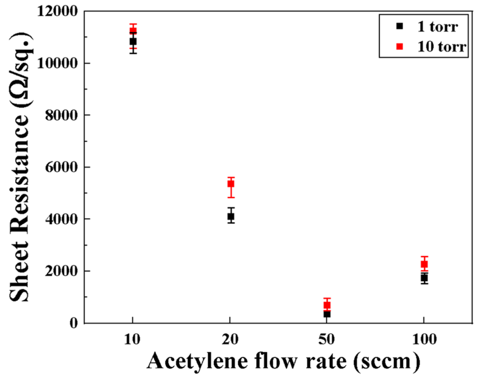
3.3. Electrical Properties (Sheet Resistance)

Figure 14 shows sheet resistance data measured on the surface of the carbon-deposited specimen according to the acetylene flow rate. Regardless of the process pressure, when the acetylene flow rate increases, the sheet resistance value decreases rapidly and then tends to increase again at 100 sccm. In the case of 10 sccm, carbon is diffused and solidified on the surface of the steel material, but since carbon is not deposited, the sheet resistance is approximately 10,000 Ω/sq, which is similar to that of a general substrate. Since carbon begins to be partially deposited at a flow rate of 20 sccm, the sheet resistance is about 4000 Ω/sq, which improves the electrical properties by more than two times. The 50 sccm condition is considered to be the condition with the best electrical properties, with a carbon structure believed to be the graphene formed and sheet resistance in the range from 300 to 800 Ω/sq. However, under the condition of 100 sccm, which has the highest flow rate, a graphite structure is deposited on the surface; therefore, the sheet resistance ranges from about 1500 to 2500 Ω/sq. The reason why electrical properties differ depending on the acetylene flow rate is due to the “patching effect,” and sheet resistance is determined by differences in microscopic defects such as cracks, grain boundaries, and holes depending on the type of carbon deposited on the surface of the steel or the number of layers within the carbon structure [37].

4. Conclusions

In this study, a thermal CVD process was performed at a high temperature of 900 °C using horizontal quartz to explain the effect of acetylene flow rate and process pressure conditions on the deposition of carbon film on the surface of iron foil. Carbon was sufficiently dissolved in the Fe lattice at high temperature, and the carbon was segregated through a cooling process to form the carbon film. By controlling the amount of carbon supplied to the surface of the specimen by changing the acetylene flow rate and process pressure, the bonding structure of the carbon film was identified, and Raman spectroscopy and HRTEM were used to evaluate the quality of the carbon film according to process conditions. Experiments under various conditions showed that as the acetylene flow rate decreased, the ID/IG ratio decreased and a higher quality carbon film was formed. In particular, in terms of mechanical and electrical properties, an appropriate acetylene flow rate (50 sccm) was confirmed to be the graphene processing condition with the best properties.

Author Contributions

Conceptualization, G.-H.K.; Methodology, G.-H.K.; Validation, Y.-K.L. and K.M.; Formal analysis, B.C.; Investigation, B.C. and Y.-K.L.; Resources, K.M.; Data curation, G.-H.K. and Y.-K.L.; Writing – original draft, G.-H.K., B.C. and K.M.; Visualization, B.C.; Supervision, Y.-K.L. and K.M.; Project administration, K.M. All authors have read and agreed to the published version of the manuscript.

Funding

This study was funded by the Korea Institute of Industrial Technology grant number KITECH KX-24-0002.

Data Availability Statement

The original contributions presented in the study are included in the article, further inquiries can be directed to the corresponding authors.

Acknowledgments

This work was supported by the R&D program of MOTIE/KICOX. This study was also supported by the Korea Institute of Industrial Technology as a “Smart Green Industrial Complex Process Innovation Simulation Center Establishment and Operation Project” (KITECH KX-24-0002).

Conflicts of Interest

The authors declare that they have no known competing financial interests or personal relationships that could have appeared to influence the work reported in this paper.

References

  1. Geim, A.K.; Novoselov, K.S. The rise of graphene. Nat. Mater. 2007, 6, 183–191. [Google Scholar] [CrossRef]
  2. Novoselov, K.S.; Geim, A.K.; Morozov, S.V.; Jiang, D.; Katsnelson, M.I.; Grigorieva, I.V.; Dubonos, S.V.; Firsovm, A.A. Two-dimensional gas of massless Dirac fermions in graphene. Nature 2005, 438, 197–200. [Google Scholar] [CrossRef] [PubMed]
  3. Novoselov, K.S.; Geim, A.K.; Morozov, S.V.; Jiang, D.; Zhang, Y.; Dubonos, S.V.; Grigorieva, I.V.; Firsov, A.A. Electric field effect in atomically thin carbon films. Science 2004, 306, 666–669. [Google Scholar] [CrossRef] [PubMed]
  4. Bhaviripudi, S.; Jia, X.T.; Dresselhaus, M.S.; Kong, J. Role of kinetic factors in chemical vapor deposition synthesis of uniform large area graphene using copper catalyst. Nano Lett. 2010, 10, 4128–4133. [Google Scholar] [CrossRef]
  5. Sun, B.; Pang, J.; Cheng, Q.; Zhang, S.; Li, Y.; Zhang, C. Synthesis of wafer-scale graphene with chemical vapor deposition for electronic device applications. Adv. Mater. Technol. 2021, 6, 2000744. [Google Scholar] [CrossRef]
  6. Wang, J.B.; Ren, Z.; Hou, Y.; Yan, X.L.; Liu, P.Z.; Zhang, H. A review of graphene synthesisatlow temperatures by CVD methods. New Carbon Mater. 2020, 35, 193–208. [Google Scholar] [CrossRef]
  7. Li, C.; Zheng, C.; Cao, F.; Zhang, Y.; Xia, X. The development trend of graphene derivatives. J. Electron. Mater. 2020, 51, 4107–4114. [Google Scholar] [CrossRef]
  8. Shi, Q.; Tokarska, K.; Ta, H.Q.; Yang, X.; Liu, Y. Substrate developments for the chemical vapor deposition synthesis of graphene. Adv. Mater. Interfaces 2020, 7, 1902024. [Google Scholar] [CrossRef]
  9. Ballestas, K.; Zapata, J.D.; Ramírez, D. Quantification of coverage, uniformity and residues for CVD monolayer graphene transfer process based on image analysis. Appl. Surf. Sci. 2023, 638, 158074. [Google Scholar] [CrossRef]
  10. Sutter, P.; Sutter, E. Microscopy of graphene growth, processing, and properties. Adv. Funct. Mater. 2013, 23, 2617–2634. [Google Scholar] [CrossRef]
  11. Yuan, Z.; He, G.; Faucher, S.; Kuehne, M.; Li, S.X. Direct chemical vapor deposition synthesis of porous single-layer graphene membranes with high gas permeances and selectivities. Adv. Mater. 2020, 33, 2104308. [Google Scholar] [CrossRef] [PubMed]
  12. Edwards, R.S.; Coleman, K.S. Graphene film growth on polycrystalline metals. Acc. Chem. Res. 2013, 46, 23–30. [Google Scholar] [CrossRef] [PubMed]
  13. Yu, Q.; Lian, J.; Siriponglert, S.; Li, H.; Chen, Y.P.; Pei, S.S. Graphene segregated on Ni surfaces and transferred to insulators. Appl. Phys. Lett. 2008, 93, 113103–113106. [Google Scholar] [CrossRef]
  14. Li, N.; Li, D.; Zhen, Z.; Zhang, R.; Mu, R.; Xu, Z. Nucleation and growth of graphene at different temperatures by plasma enhanced chemical vapor deposition. Mater. Today Commun. 2023, 36, 106568. [Google Scholar] [CrossRef]
  15. Fang, W.; Hsu, A.L.; Song, Y.; Birdwell, A.G.; Amani, M.; Dubey, M.; Dresselhaus, M.S.; Palacios, T.; Kong, J. Asymmetric growth of bilayer graphene on copper enclosures using low-pressure chemical vapor deposition. ACS Nano 2014, 8, 6491–6499. [Google Scholar] [CrossRef]
  16. Zhao, Z.; Shan, Z.; Zhang, C.; Li, Q.; Tian, B.; Huang, Z.; Lin, W.; Chen, X.; Ji, H.; Zhang, W.; et al. Study on the diffusion mechanism of graphene grown on copper pockets. Small 2015, 11, 1418–1422. [Google Scholar] [CrossRef]
  17. Addou, R.; Dahal, A.; Sutter, P.; Batzill, M. Monolayer graphene growth on Ni(111) by low temperature chemical vapor deposition. Appl. Phys. Lett. 2012, 100, 21601. [Google Scholar] [CrossRef]
  18. Ramón, M.E.; Gupta, A.; Corbet, C.; Ferrer, D.A.; Movva, H.C.P.; Carpenter, G.; Colombo, L.; Bourianoff, G.; Doczy, M.; Akinwande, D.; et al. CMOS-compatible synthesis of large-area, high-mobility graphene by chemical vapor deposition of acetylene on cobalt thin films. ACS Nano 2011, 5, 7198–7204. [Google Scholar] [CrossRef]
  19. Kwon, S.Y.; Ciobanu, C.V.; Petrova, V.; Shenoy, V.B.; Bareño, J.; Gambin, V.; Petrov, I.; Kodambaka, S. Growth of semiconducting graphene on palladium. Nano Lett. 2009, 9, 3985–3990. [Google Scholar] [CrossRef] [PubMed]
  20. Murata, Y.; Starodub, E.; Kappes, B.B.; Ciobanu, C.V.; Bartelt, N.C.; McCarty, K.F.; Kodambaka, S. Orientation-dependent work function of graphene on Pd (111). Appl. Phys. Lett. 2010, 97, 143114. [Google Scholar] [CrossRef]
  21. Xue, Y.; Wu, B.; Guo, Y.; Huang, L.; Jiang, L.; Chen, J.; Geng, D.; Liu, Y.; Hu, W.; Yu, G. Synthesis of large-area, few-layer graphene on iron foil by chemical vapor deposition. Nano Res. 2011, 4, 1208–1214. [Google Scholar] [CrossRef]
  22. Lee, J.H.; Lee, E.K.; Joo, W.-J.; Jang, Y.; Kim, B.-S.; Lim, J.Y.; Choi, S.-H.; Ahn, S.J.; Ahn, J.R.; Park, M.-H.; et al. Wafer-scale growth of single-crystal monolayer graphene on reusable hydrogen-terminated germanium. Science 2014, 344, 286–289. [Google Scholar] [CrossRef] [PubMed]
  23. Wang, G.; Zhang, M.; Zhu, Y.; Ding, G.; Jiang, D.; Guo, Q.; Liu, S.; Xie, X.; Chu, P.K.; Di, Z.; et al. Direct growth of graphene film on germanium substrate. Sci. Rep. 2013, 3, 2465. [Google Scholar] [CrossRef]
  24. An, H.; Lee, W.J.; Jung, J. Graphene synthesis on Fe foil using thermal CVD. Curr. Appl. Phys. 2011, 11, S81–S85. [Google Scholar] [CrossRef]
  25. Chen, W.Q.; Cheong, Y.H.; Fu, X.; Ge, L.Y.; Veksha, A.; Lisak, G. Fe-assisted catalytic chemical vapor deposition of graphene-like carbon nanosheets over SrO. Carbon 2021, 171, 444–454. [Google Scholar] [CrossRef]
  26. Medina-Llamas, V.L.; Fajardo-Díaz, J.L.; Morelos-Gomez, A.; Endo, M.; López-Urías, F.; Muñoz-Sandoval, E. Crystalline multilayer graphene nanoflakes synthesized by catalytic chemical vapor deposition using reduced nanostructured hematite as catalyst precursor and 1,2-dichlorobenzene and benzylamine mixture as carbon source. Carbon 2023, 203, 813–826. [Google Scholar] [CrossRef]
  27. Losurdo, M.; Giangregorio, M.M.; Capezzuto, P.; Bruno, G. Graphene CVD growth on copper and nickel: Role of hydrogen in kinetics and structure. Phys. Chem. Chem. Phys. 2011, 13, 20836–20843. [Google Scholar] [CrossRef]
  28. Sun, X.; Lin, L.; Sun, L.; Zhang, J.; Rui, D.; Li, J.; Wang, M.; Tan, C.; Kang, N.; Wei, D.; et al. Low-temperature and rapid growth of large single-crystalline graphene with ethane. Small 2018, 14, 1702916. [Google Scholar] [CrossRef]
  29. Chen, C.S.; Hsieh, C.K. Effects of acetylene flow rate and processing temperature on graphene films grown by thermal chemical vapor deposition. Thin Solid Films 2015, 584, 265–269. [Google Scholar] [CrossRef]
  30. Allen, M.J.; Tung, V.C.; Kaner, R.B. Honeycomb Carbon: A Review of Graphene. Chem. Rev. 2010, 110, 132–145. [Google Scholar] [CrossRef]
  31. Hbiriq, Y.; Ammar, M.R.; Fantini, C.; Hennet, L.; Zaghrioui, M. Probing symmetry-breaking defects in polished graphitizable s p 2 carbons using angle-resolved polarized Raman scattering. Phys. Rev. B 2023, 107, 134305. [Google Scholar] [CrossRef]
  32. Haridas, H.; Kader, A.K.A.; Sellathurai, A.; Barz, D.P.; Kontopoulou, M. Noncovalent Functionalization of Graphene Nanoplatelets and Their Applications in Supercapacitors. ACS Appl. Mater. Interfaces 2024, 16, 16630–16640. [Google Scholar] [CrossRef] [PubMed]
  33. Castriota, M.; Cazzanelli, E.; Pacilè, D.; Papagno, L.; Girit, O.; Meyer, J.C.; Zettl, A.; Giarola, M.; Mariotto, G. Spatial dependence of Raman frequencies in ordered and disordered monolayer graphene. Diamond Relat. Mater. 2010, 19, 608. [Google Scholar] [CrossRef]
  34. Ferrari, A.C.; Meyer, J.C.; Scardaci, V.; Casiraghi, C.; Lazzeri, M.; Mauri, F.; Piscanec, S.; Jiang, D.; Novoselov, K.S.; Roth, S.; et al. Raman spectrum of graphene and graphene layers. Rev. Lett. 2006, 97, 187401. [Google Scholar] [CrossRef] [PubMed]
  35. Liu, K.; Lu, F.; Li, K.; Xu, Y.; Ma, C. Synthesis of turbostratic graphene by direct carbon ions implantation on LiNbO3. Appl. Surf. Sci. 2019, 493, 1255–1259. [Google Scholar] [CrossRef]
  36. Garlow, J.A.; Barrett, L.K.; Wu, L.; Kisslinger, K.; Zhu, Y.; Pulecio, J.F. Large-Area Growth of Turbostratic Graphene on Ni (111) via Physical Vapor Deposition. Sci. Rep. 2016, 6, 19804. [Google Scholar] [CrossRef]
  37. Yu, Q.; Jauregui, L.A.; Wu, W.; Colby, R.; Tian, J.; Su, Z.; Cao, H.; Liu, Z.; Pandey, D.; Wei, D.; et al. Control and characterization of individual grains and grain boundaries in graphene grown by chemical vapour deposition. Nat. Mater. 2011, 10, 443–449. [Google Scholar] [CrossRef]
Figure 1. Carbon allotrope formation mechanism on iron (Fe) substrate for CVD process.
Crystals 14 00782 g001
Figure 2. Schematic of CVD graphene growth process using acetylene as the carbon source.
Crystals 14 00782 g002
Figure 3. Process schedule of CVD graphene growth process.
Crystals 14 00782 g003
Figure 4. Top views of carbon synthesized specimens according to flow rates at 10 torr: (a) 10 sccm; (b) 20 sccm; (c) 50 sccm; (d) 100 sccm.
Crystals 14 00782 g004
Figure 5. Optical images of deposited carbon on iron (Fe) substrates at different flow rates: (a) 10 sccm; (b) 20 sccm; (c) 50 sccm; (d) 100 sccm. The process pressure was set to 1 torr.
Crystals 14 00782 g005
Figure 6. Optical images of deposited carbon on iron (Fe) substrates at different flow rates: (a) 10 sccm; (b) 20 sccm; (c) 50 sccm; (d) 100 sccm. The process pressure was set to 10 torr.
Crystals 14 00782 g006
Figure 7. (a) Optical microscope image of carbon deposited under 20 sccm, 10 torr; (b) corresponding Raman spectra to the located area.
Crystals 14 00782 g007
Figure 8. XPS spectra of C1s of graphene and graphite deposited under 20 sccm, 10 Torr; (a) dark gray C area; (b) black D area.
Crystals 14 00782 g008
Figure 9. AFM images of carbon layer under 20 sccm, 10 torr, with the height profiles of the lines being shown on the bottom of each image: (a) dark gray area; (b) black area.
Crystals 14 00782 g009
Figure 10. SEM images of as-deposited layers at 20 sccm C2H2, 10 torr: (a) A-B boundary; (b) A zone; (c) B zone.
Crystals 14 00782 g010
Figure 11. Raman spectra of graphene grown on AISI 1006 foil at 900 °C according to flow rates: (a) 1 torr; (b) 10 torr.
Crystals 14 00782 g011
Figure 12. HRTEM images of graphene films grown according to acetylene flow rates: (a) 20 sccm; (b) 50 sccm; (c) 100 sccm. The process pressure was set to 10 torr.
Crystals 14 00782 g012
Figure 13. Hardness in surface of substrate- and carbon-deposited specimens according to the position of deposited layers: (a) micro-Vickers hardness; (b) nano-indentation hardness.
Crystals 14 00782 g013
Figure 14. Sheet resistances of the carbon synthesized specimens at different flow rates and pressures.
Crystals 14 00782 g014
Table 1. Carbon solubility and the growth mechanism according to transition metals for CVD graphene.
Transition MetalCarbon Solubility at 1000 °CGrowth Mechanism
Copper (Cu)0.03 wt.%Penetration [15,16]
Nickel (Ni)2.02 wt.%Surface deposition [17]
Cobalt (Co)3.41 wt.%Segregation [18]
Platinum (Pd)5.98 wt.%Segregation [19,20]
Iron (Fe)7.91 wt.%Segregation [21]
Germanium (Ge)0.00 wt.%Surface deposition [22,23]
Table 2. Chemical composition of AISI 1006 steel (wt.%).
wt.%CSiMnPSNiCrMo
AISI 10060.0490.0030.2320.0130.0080.0850.0560.041
Disclaimer/Publisher’s Note: The statements, opinions and data contained in all publications are solely those of the individual author(s) and contributor(s) and not of MDPI and/or the editor(s). MDPI and/or the editor(s) disclaim responsibility for any injury to people or property resulting from any ideas, methods, instructions or products referred to in the content.

