Article

Electronic Structure and Optical Properties of GaAs Doped with Rare-Earth Elements (Sc, Y, La, Ce, and Pr)

1
Guizhou Vocational College of Foodstuff Engineering, Guiyang 550000, China
2
School of Electronics and Information Engineering, Anshun University, Anshun 561000, China
*
Author to whom correspondence should be addressed.
Crystals 2025, 15(1), 98; https://doi.org/10.3390/cryst15010098
Submission received: 11 November 2024 / Revised: 5 January 2025 / Accepted: 7 January 2025 / Published: 20 January 2025
(This article belongs to the Special Issue Rare Earths-Doped Materials (3rd Edition))

Abstract

:
Herein, the electronic structure and optical properties of GaAs doped with rare-earth elements (Sc, Y, La, Ce, and Pr) were evaluated using the first-principles method. Results showed that the lattice constants and cell volume of GaAs increased after doping. Band structure calculations indicated that the lowest conduction band and highest valence band were evident at the G-point, demonstrating that rare-earth-element doping did not alter the material type of GaAs, which remained a direct-bandgap semiconductor. The bandgap of Sc-doped GaAs increased, whereas those of Y-, La-, Ce-, and Pr-doped GaAs decreased. Moreover, the density of energy levels increased. Doping with Ce and Pr introduced impurity levels, and the Fermi level shifted into the conduction band. Investigation of the optical properties revealed that the static dielectric constant increased with La doping but decreased with Y, La, Ce, and Pr doping. The variation trends of the extinction coefficients of the doped samples were consistent with that of undoped GaAs: the extinction coefficient shifted to a low-energy region. In addition, a slight redshift occurred in the absorption spectrum. The absorption peak also diminished owing to rare-earth-element doping. We concluded that Ce- and Pr-doped GaAs can form metal alloys with different compositions. Such doping may provide a new class of materials for use in optoelectronic devices.

1. Introduction

GaAs is an important second-generation semiconductor material used in optoelectronics. It offers several advantages, including a direct bandgap of 1.424 eV [1,2], high charge-carrier mobility (8800 cm2v−1s−1) [3,4], low power consumption, and strong radiation resistance. However, undoped GaAs exhibits a low absorption rate for infrared light and low photoelectric conversion efficiency and has a limited practical application range [5,6,7,8,9,10].
Doping is an important way to control material properties. Through doping, the electronic structures of materials can be modulated; electrical, optical, and magnetic properties of semiconductors can be regulated; and photoelectric materials with desired electronic structures and optical properties can be obtained. Ma et al. [11] investigated the electronic structure and optical properties of CuxGa1−xAs (x = 3.125%, 6.25%, and 12.5%), a compound exhibiting a sphalerite structure. Their results indicated that with increasing Cu doping, the static dielectric constant and refractive index of the doped system increased, the absorption spectrum redshifted, and light absorption increased. Xiong et al. [12] examined the electronic structure and optical properties of GaAs doped with transition metals Mn, Fe, and Co. They found the absorption coefficients of GaAs samples in infrared and near-infrared regions to be substantially improved after doping. Notably, the magnetic properties of Mn-doped GaAs primarily resulted from Mn [13]. Further, GaAs showed a ferromagnetic nature when doped with Mn at a concentration of 6.25% [12]. Various researchers have doped GaAs with Pt, Ag, Al, Au, In, Sb, Fe, P, Cr, and other elements, achieving remarkable improvements in material properties [14,15,16,17,18,19,20,21]. In particular, GaAsBi exhibits potential for application in long-wave emitters, detectors, and spintronic devices. At present, GaAsBi has been successfully prepared via metal–organic chemical vapor deposition [22,23,24] and molecular beam epitaxy (MBE) [23,25,26,27]. Notably, Bi doping causes an inherent tradeoff in charge-carrier mobility [28]. The increase in Bi concentration plays an important role in the modulating hole mobility [29], optical absorption coefficient, refractive index, and static dielectric constant. Studying the electronic and optical properties of semiconductor alloys provides an efficient method for customizing the former properties of materials as per the needs of practical electronics. InGaAs features a high charge-carrier mobility, high stability, and good radiation resistance. Further, it is widely used in optical fiber communication, photovoltaic power generation, and infrared light detection applications [20]. Currently, there are numerous theoretical and experimental research reports on InGaAs. For instance, Paul et al. [18] derived empirical formulas for the relationship between x in InxGa1−xAs systems and parameters such as the bandgap and charge-carrier concentration. Ma et al. [17] investigated the qualitative relationship between the In doping and photoelectric properties of In-doped GaAs. The ternary semiconductor alloy BxGa1−xAs alloy has been successfully grown by MBE and metal–organic chemical vapor deposition (MOCVD). This alloy has been used in light emitters or detectors and in solar cell applications [30]. Further, it is widely used in high-temperature applications and electro-optical devices in the short-wavelength range of the visible spectrum. The alloy can be grown on Si and GaAs substrates without strain mismatch, making it very attractive for next-generation optoelectronic and microelectronic devices.
El-Jaroudi et al. added In into the BGaAs alloy to extend its emission wavelength. BGaAs is a poor emitter because of the presence of B cluster states. The incorporation of In lowered the conduction band edge down to B cluster states [31], leading to a high internal quantum efficiency. The simultaneous incorporation of In and B broadened the emission wavelength, which was beneficial for Si-based optoelectronic devices. Geisz et al. [32] found that GaInAs alloy can be tuned to lattice-match to GaAs and Si with a bandgap smaller than that of GaAs. This alloy shows excellent electrical conductivity and corrosion resistance and is widely used in aerospace, electronics, communication, and other fields. In addition, alloys such as GaAsN, AlGaAs, and GaAsNBi [33] are of great importance for high-efficiency solar cells and infrared laser applications.
Rare-earth elements have unique electronic structures, enabling effective regulation of the electronic structures and optical properties of materials prepared from them. By doping rare-earth elements, such as Pr, Nd, and Yb, into GaAs, Rzakuliev et al. [34] achieved the photoluminescence of Pr and Nd. Ennen et al. [35] and Taguchi et al. [36] observed Yb 4f photoluminescence in Yb-doped GaAs using the Hall effect and deep-level transient spectroscopy measurements, respectively, proposing that Yb doping generated deep electron traps in GaAs. Thus, investigations of the electrical and optical properties of Yb-doped GaAs can help elucidate the excitation mechanism of the rare-earth-element 4f shell.
Seghier et al. [37] performed photoluminescence (PL) spectroscopy, photoinduced current transient spectroscopy (PICTS), and photoconductivity (PC) measurements on Yb (Er)-doped GaAs grown via MBE. Burke et al. [38] examined the role of Er as an atomic dopant in GaAs, In0.53Ga0.47As, and InAs. Several Er-doped samples were grown via MBE, and their electrical properties were studied via Hall effect measurements. Li et al. [39] theoretically calculated the bandgap and determined the absorption spectrum of Pr-doped GaAs using the pseudopotential plane-wave approach and found that the 4f electrons of Pr reduced the bandgap of GaAs and redshifted its absorption spectrum. Svane et al. [33] evaluated rare-earth-doped GaAs and GaN. Total energy calculations reveal Ga substitution as the most favorable rare-earth defect, with the rare-earth ion taking the isoelectronic trivalent configuration in all cases studied. The photoelectric properties of CdS doped with rare-earth metals such as Sc, Y, and La have been studied [40], revealing that the rare-earth metals provided additional charge carriers at the Fermi level. The metals improved the electronic structures and considerably decreased the static dielectric constant, absorption coefficient, and reflectivity, effectively modulating the photoelectric properties of CdS. The photoelectric properties of La- and Y-doped Ca–Si were also investigated [41], revealing that La and Y changed the material type of Ca2Si to n-type and the extinction coefficient, and the absorption edge shifted toward low energies. Meanwhile, the refractive index and reflectivity increased. The electronic structure and optical properties of β-FeSi2 doped with La, Y, and Ce were also investigated [42], which revealed that the volume of the lattice reduces. The band structure near the gap becomes complex, and the bandgap becomes narrow obviously. The static dielectric constant increases, the peak of the imaginary part of dielectric function ε2 decreases and moves to a lower energy, the refractive index n0 increases significantly, and the peak of k decreases. Wang et al. [43] studied the effects of La and Ce doping on the electronic structure and optical properties of Mn4Si7. The results revealed that the doping of the rare-earth elements improved the static dielectric constant and light absorption performance. Zhao et al. [44] studied the photoelectric performance of NaTaO3 doped with lanthanide elements such as Ce, Pr, Nd, Sm, and Eu. The results showed that these elements effectively blocked the recombination of photogenerated electrons and holes in the material and improved its photocatalytic performance. In summary, materials doped with rare-earth elements have excellent optical, electrical, magnetic, and catalytic properties. Rare-earth-element doping is expected to improve the visible-light absorption ability of GaAs, inhibit the recombination of photogenerated electrons and holes, and improve the photocatalytic performance of GaAs.
In this paper, an improvement in the photoelectric properties of GaAs doped with Sc, Y, La, Ce, and Pr was studied via first-principles calculations. The results showed that the static dielectric constant of GaAs increased after La doping and decreased after doping other rare-earth elements. Further, the extinction coefficient shifted slightly to the low-energy region, the absorption edge of the spectrum slightly redshifted, and the absorption peaks weakened. The lattice constants and cell volume increased after rare-earth-element doping. Moreover, Sc doping increased the bandgap, while Y, La, Ce, and Pr doping densified the energy levels and decreased the bandgap. Doping with Ce and Pr introduced impurities because their 4f orbital electrons formed a narrow f-band close to the conduction band minimum that was filled with an electron. Based on Svane et al.’s calculations [33], we concluded that Ce- and Pr-doped GaAs can form metal alloys with different compositions. Such doping may provide a new class of materials for use in optoelectronic devices.

2. Models and Methods

GaAs belongs to the cubic crystal system, with the space group being F-43 m and lattice constants being a = b = c = 0.5653 nm [45]. Each unit cell of GaAs contains four Ga atoms and four As atoms. Herein, a 2 × 2 × 2 supercell structure comprising 64 atoms was used. The central Ga (blue) atom in the supercell was replaced by a Sc, Y, La, Ce, or Pr atom to construct a doping model (Figure 1).
To ensure the convergence of the calculation results, a K-point convergence test was used with a cutoff energy of 500 eV within a grid range from 1 × 1 × 1 to 7 × 7 × 7. The total energy began to converge when the K-point sampling grid was 2 × 2 × 2. A K-point grid of 4 × 4 × 4 was employed to achieve a higher density of K points. Figure 2 presents the results of the K-point convergence test.
All calculations were performed using the CASTEP8.0 [46] software package. The lattice constants were initially optimized using the BFGS algorithm. Local density approximation was used for the exchange–correlation potential, and the interaction between the ions and valence-shell electrons was represented using the ultrasoft pseudopotential. The valence-electron configurations selected were as follows: Sc: 3s23p63d14s2, Y: 4s24p64d15s2, La: 5s25p65d16s2, Ce: 4f15s25p65d16s2, Pr: 4f35s25p66s2, Ga: 3d104s24p1, and As: 4s24p3. A 4 × 4 × 4 Monkhorst–Pack mesh, which exhibits high symmetry, was employed to represent the Brillouin region, with a plane-wave phase of 400 eV.

3. Results and Analysis

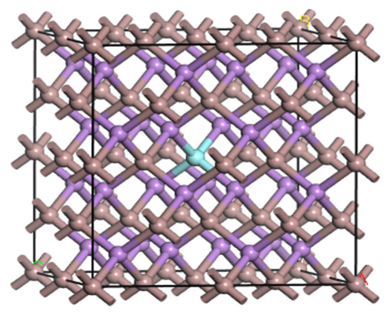
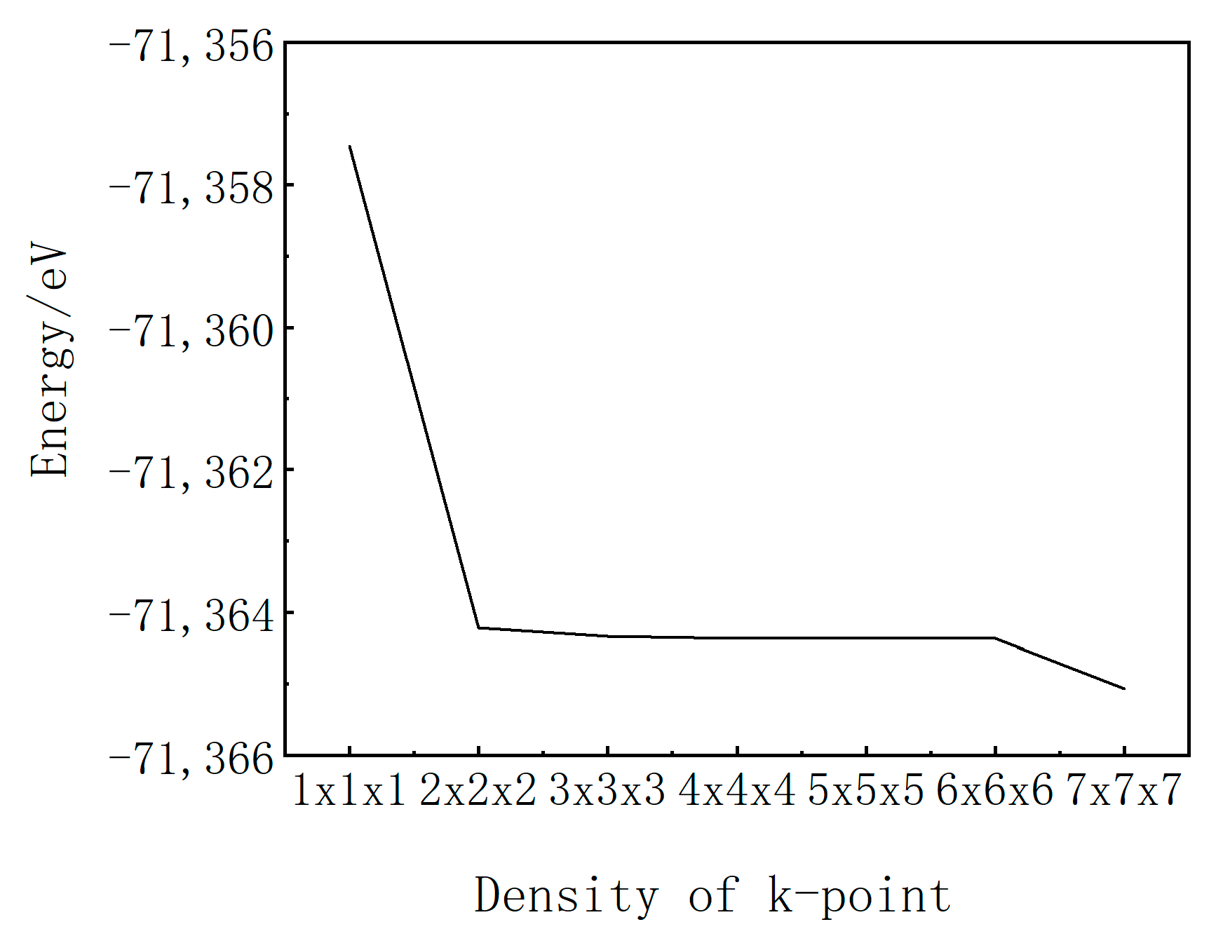
3.1. Geometric Structure Optimization

Intrinsic GaAs and GaAs doped with Sc, Y, La, Ce, and Pr were geometrically optimized. Subsequently, the lattice constants, cell volume, and total energy were calculated (Table 1). Notably, the difference between the calculated and experimental lattice constants of GaAs was 7.9 × 10⁻³ nm, with an error of 1.3%, which was within the acceptable error range. This discrepancy was due to the inherent limitations of the calculation method. Nevertheless, the low error confirmed the accuracy of the selected parameters and method. The lattice constant increased upon doping with Sc, Y, La, Ce, and Pr because the ionic radii of these elements were larger than that of Ga, increasing the cell volume. The most notable cell volume expansion occurred after La doping. Doping was found to disrupt the GaAs lattice periodicity. Consequently, the lattice was stretched, leading to internal distortion. From a total-energy perspective, rare-earth-element doping increased the system energy, with La and Pr doping leading to the highest and lowest system energies, respectively. This finding suggested that the Pr-doped system was the most stable.

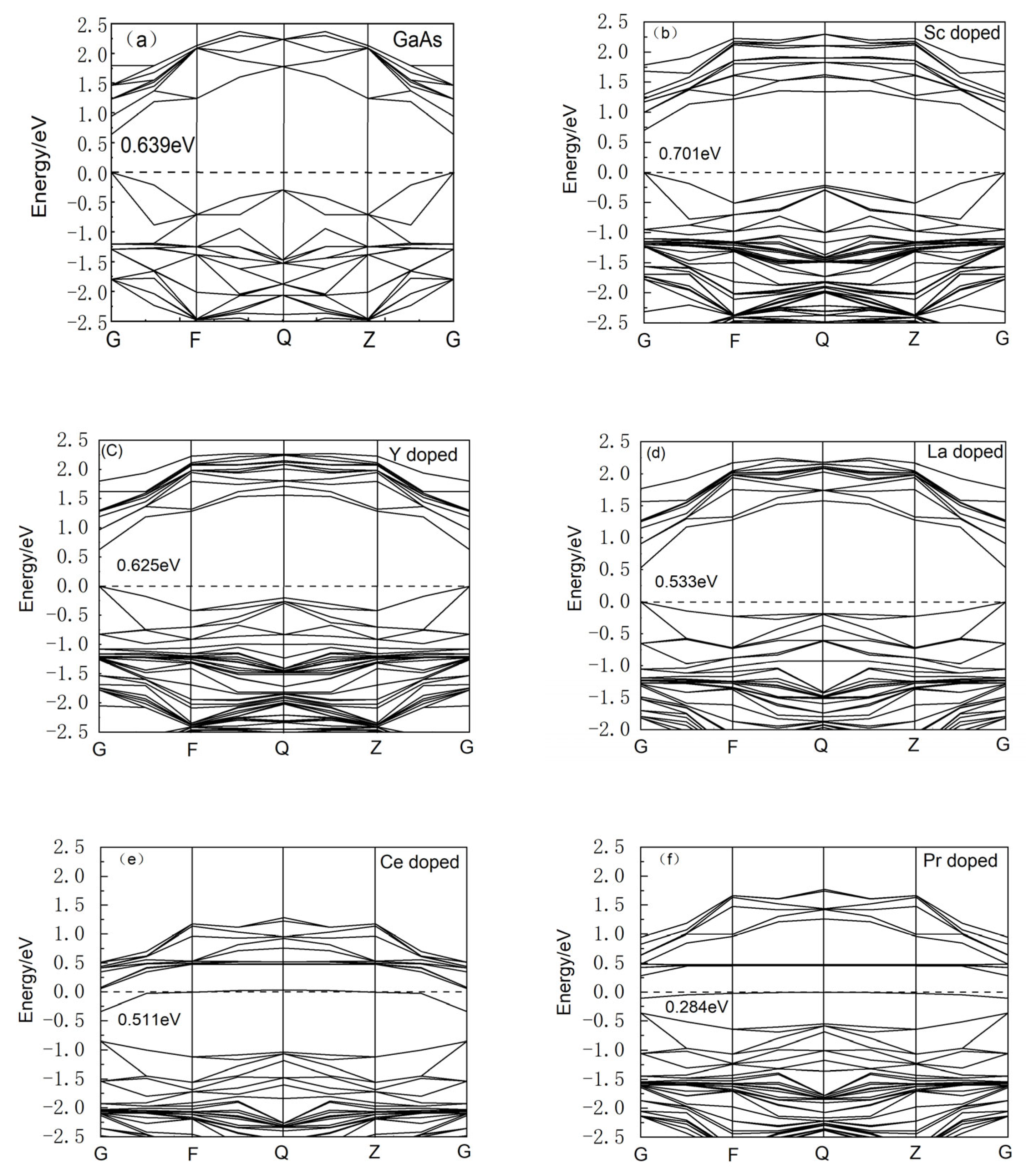
3.2. Band Structure and Density of States
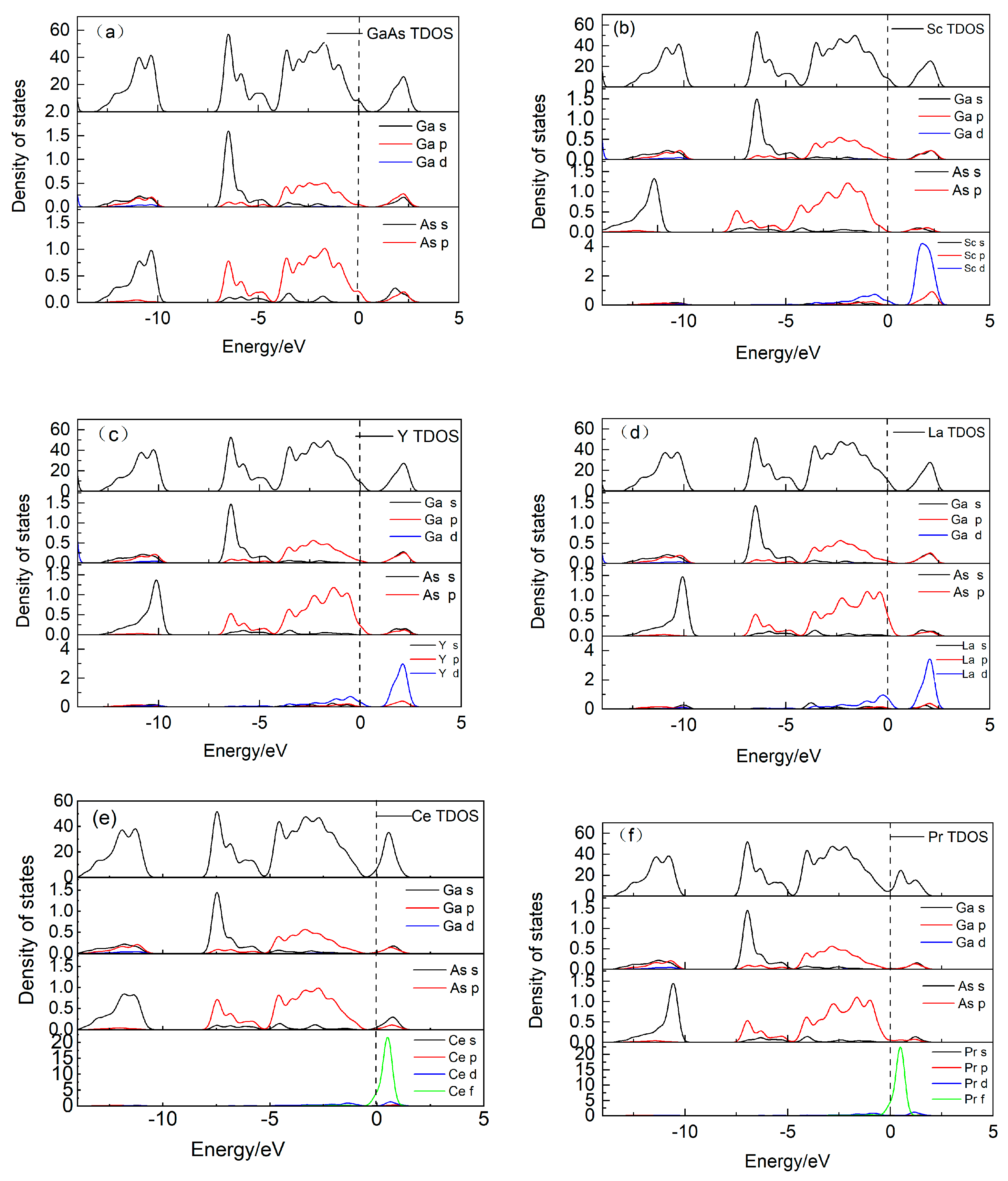
Figure 3 presents the energy-band structure of undoped and rare-earth-element-doped GaAs. The diagram focuses on an energy range of −2.5 to 2.5 eV because the characteristics of the energy-band structure are primarily determined by the bands present near the Fermi level. The dashed line in the figure indicates the Fermi level, which is set as the energy zero. As shown in Figure 3a, the conduction band minimum and valence band maximum of undoped GaAs are obvious at the G-point, confirming that it is a direct-bandgap semiconductor with a bandgap of 0.639 eV. This value is consistent with that reported by Xiong et al. [12] but lower than the experimental value of 1.42 eV due to the estimation error of the density functional. Nevertheless, this discrepancy does not affect the analysis of the sample properties.
Figure 3 demonstrates that after doping with Sc, Y, La, Ce, and Pr, the conduction band minimum and valence band maximum are located at the G-point, indicating that rare-earth-element doping did not alter the material type of GaAs, which is still a direct-bandgap semiconductor. As shown in Figure 3b, after Sc doping, the conduction band increased, the bandgap widened, and the distribution region of the conduction and valence bands changed. These alterations increased the electron concentration near the bandgap, increasing their transition probability. This indicated that energy-level splitting occurred after Sc doping, more tracks were available near the bandgap, and the bandgap widened, increasing the energy required for valence band electrons to transition to the conduction band. Thus, electron transition became more difficult than that in the case of the undoped system. Figure 3c,d illustrate that after the incorporation of Y and La, the bandgap increases to 0.625 and 0.533 eV, respectively, and the distribution region of the conduction and valence band changes, reducing the energy required for electron transition from the valence band to the conduction band. Moreover, electron transition in the doped systems becomes easier than that in the undoped system. Figure 3e,f show that after Ce and Pr doping, the conduction and valence bands shift downward and the Fermi level shifts toward the conduction band, indicating the characteristics of n-type semiconductors. This is because the 4f orbital energy states of Ce and Pr introduce impurity levels in the bandgap. The conduction and valence bands move down considerably, consistent with the calculation results reported by Li et al. [39]. The radii and properties of Ce and Pr are considerably different from those of Ga. After doping, the integrity of the original crystal is destroyed and a crystal field is formed around the impurity due to electrical imbalance. This field destroys the periodic potential field of the crystal, resulting in localized electronic energy states and impurity energy levels in the bandgap [43]. These impurity levels enlarge the effective bandgap of doped materials, reducing the excitation energy required for electron transition from the valence band to the conduction band. In other words, electrons can only absorb photons in the infrared region to transition to impurity levels and absorb photons with lower energies to transition to the conduction band [46]. This step-wise transition improves the long-wave absorption ability of materials, resulting in a photoelectric effect that endows the materials with the ability to absorb light waves with long wavelengths. Thus, Ce and Pr doping facilitated the easy transition of valence electrons, reducing the energy required for transition. Consequently, the absorption edge of the optical absorption spectrum was redshifted, thereby improving the photocatalytic efficiency of the doped materials.

Density of States

Figure 4a presents the density of states of undoped GaAs. The valence band of undoped GaAs near the Fermi level primarily comprises Ga-4p and As-4p states and the conduction band comprises Ga-4p, Ga-4S, As-4p, and As-4s states.
Figure 4b–d show the density of states of undoped and Sc-, Y-, and La-doped GaAs. The figures reveal that the valence band near the Fermi level is primarily composed of Ga-4p and As-4p states and a few electronic states are provided by Sc-3d, Y-4d, and La-5d states. The conduction band comprises Ga-4p, Ga-4s, As-4p, and As-4s states as well as Sc-3d, Y-4d, and La-5d states generated after doping. Sc doping causes the As-4p electrons to move toward the valence band edge, modifying the bandgap, consistent with the band analysis. With Y doping, the density of states remains the same as that of undoped GaAs; however, the bandgap slightly narrows. Following La doping, the As-4p electron moves towards the conduction band, further narrowing the bandgap.
As shown in Figure 4e,f, after Ce and Pr doping, the valence and conduction bands shift downward. The valence band near the Fermi level mainly comprises Ga-4p and As-4p electron states, with an increased density of states and reduced localization owing to Ce and Pr doping. The conduction band comprises Ga-4p, Ga-4s, As-4p, and As-4s states, along with the 4f electron energy states of Ce and Pr. Notably, 4f electron energy states cause the conduction band to narrow, enhancing localization.

3.3. Optical Properties

The electronic structure of a crystal is closely related to its optical properties, and the optical response of a material is usually expressed by a complex dielectric function ε(ω) = ε1(ω) + ε2(ω) in the linear range. ε2(ω) is determined by calculating the transition energy between occupied and unoccupied electron orbitals, and ε1(ω) is obtained from the Kramers–Kronig dispersion relation. Then, the absorption rate, refractive index, and reflectivity of the material are derived.

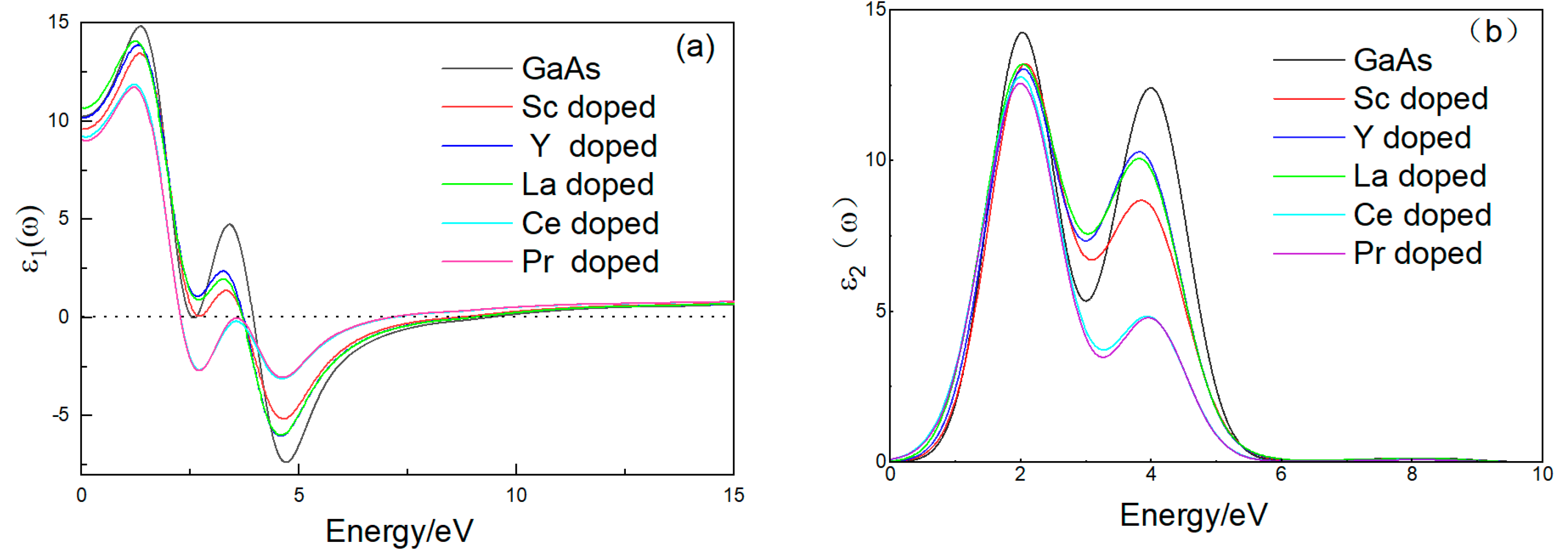
3.3.1. Dielectric Function

Figure 5 shows the dielectric function of undoped GaAs and GaAs doped with Sc, Y, La, Ce, and Pr. The ε(ω) usually represents the polarization and charge-binding ability of a system. A large real part of the dielectric constant indicates strong polarization and high charge-binding ability. The static dielectric constants of undoped GaAs and GaAs doped with Sc, Y, La, Ce, and Pr were as follows: 10.23 for undoped GaAs and 9.60, 10.18, 10.68, 9.26, and 9.09 for GaAs doped with Sc, Y, La, Ce, and Pr, respectively (Figure 5a). The static permittivity increased after La doping but decreased after Pr doping. In addition, the polarization ability of La-doped GaAs enhanced, and the transport rate of photogenerated carriers increased. Meanwhile, doping with Sc, Y, Ce, and Pr reduced the polarization ability of GaAs, with Pr showing the highest reduction effect, hindering the migration and separation of photogenerated electron–hole pairs. For undoped GaAs, two peaks were observed at 1.36 and 3.40 eV, with amplitudes of 14.83 and 4.74 eV, respectively. The peak amplitudes of Sc-, Y-, La-, Ce-, and Pr-doped GaAs decreased compared to those of undoped GaAs.
The imaginary component of the dielectric function reflects the probability of electron excitation transitions in semiconductor materials. A large value of the imaginary component indicates increased electrons in excited states, indicating an increased probability of further transitions. Figure 5b shows the imaginary components of the dielectric functions of doped GaAs samples, showing that at a photon energy of 0 eV, the components move slightly toward low energies. Compared with the peaks of undoped GaAs at 2.02 and 3.99 eV, those in the case of doped GaAs samples have lower intensities; in addition, the second peak shifts toward low energies after doping. This finding suggests that rare-earth-element doping leads to numerous conduction electrons at the Fermi level, changes electron transition characteristics between bands, and affects the GaAs nodal functions and optical properties.

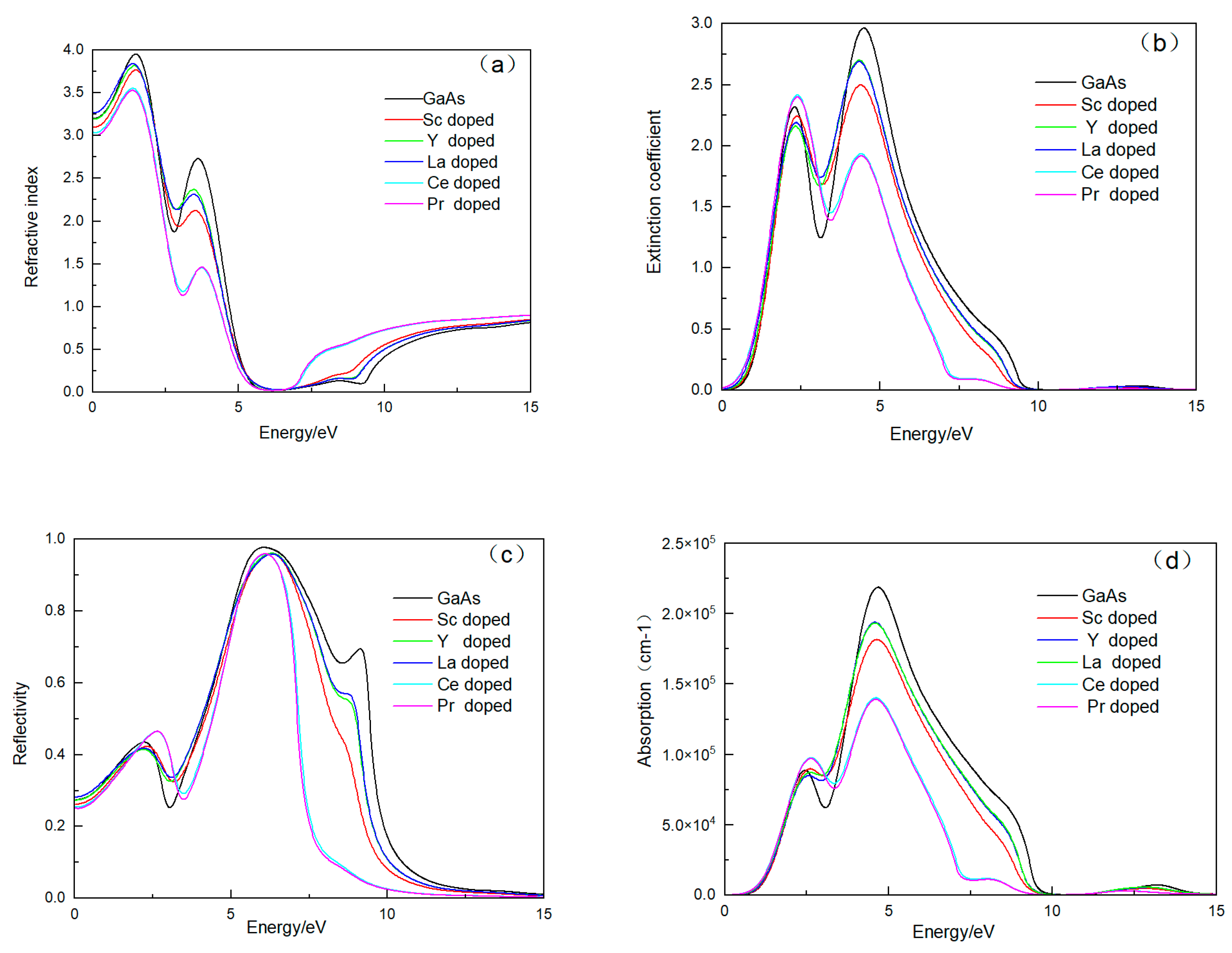
3.3.2. Refractive Index, Reflection Spectrum, and Absorption Coefficient

Figure 6a,b show the complex refractive indices of GaAs doped with Sc, Y, La, Ce, and Pr. Figure 6a demonstrates that the average refractive index of undoped GaAs is 3.19 and that it peaks at 1.47 and 3.61 eV, with the peak values being 3.95 and 2.73, respectively. After doping with Y, the average refractive index remained mostly unchanged; meanwhile, La doping resulted in an increment to 3.26, whereas Sc, Ce, and Pr doping resulted in decrements to 3.09, 3.04, and 3.01, respectively. Notably, Pr doping led to the most notable reduction in the two values. In an energy range of 7–12 eV, the peak refractive-index values of the doped GaAs samples were higher than those of undoped GaAs, with Ce- and Pr-doped GaAs exhibiting a third refractive-index peak.
Figure 6b suggests that the change trend of the extinction coefficient after doping with Sc, Y, La, Ce, and Pr is consistent with that of undoped GaAs, with a slight shift toward the low-energy region. Extinction coefficients of the Ce- and Pr-doped samples at the first peak were higher than that in the case of undoped GaAs, whereas the second peak exhibited the lowest extinction coefficient. The extinction coefficients of GaAs doped with Sc, Y, and La were lower than those of undoped GaAs at the first and second peaks.
Figure 6c shows that compared with undoped GaAs, GaAs doped with Sc, Y, La, Ce, and Pr exhibits lower utilization ratios in the infrared region, with Ce and Pr doping leading to the lowest values. This finding indicates that Ce and Pr doping lead to the lowest improvement in the photocatalytic effect of GaAs. In addition, the average and maximum reflectivities of GaAs decrease after doping, with Ce and Pr doping causing the most remarkable reductions. This result suggests that the metallic reflection characteristics of GaAs are weakened by these dopants.
Figure 6d presents the absorption spectra of undoped GaAs and GaAs doped with Sc, Y, La, Ce, and Pr. The absorption edge slightly redshifts after rare-earth-element doping, consistent with the energy-band analysis results. Moreover, the spectrum range narrows, with the smallest range observed after Ce and Pr doping, consistent with changes observed in the dielectric function. Compared with undoped GaAs, GaAs doped with Sc, Ce, or Pr exhibits a higher absorption coefficient at the first absorption peak, whereas GaAs samples doped with Y or La exhibit slightly lower values. Meanwhile, at the second absorption peak, all the rare-earth elements lead to lower absorption coefficients than that of undoped GaAs, with Ce and Pr resulting in the largest reduction. In particular, the second-peak absorption coefficient of undoped GaAs (218,809.45 cm−1) is reduced to 140,136.31 and 139,157.11 cm−1 after doping with Ce and Pr, respectively. This reduction in the peak values indicates that the transition process of valence electrons from the conduction band to the excited state is weakened, diminishing the visible-light response of GaAs after Sc, Y, La, Ce, and Pr doping.

4. Conclusions

Herein, the electronic structure and optical properties of GaAs doped with Sc, Y, La, Ce, and Pr were evaluated using the first-principles method. The results revealed that the lattice constants and cell volume increased after doping. Sc doping increased the bandgap while Y, La, Ce, and Pr doping decreased the bandgap and led to a denser energy-level distribution. The incorporation of Ce and Pr caused the conduction and valence bands to move downward, creating impurity levels influenced by the 4f electrons of Ce and Pr. Consequently, a narrowed conduction band and enhanced localization were achieved. Investigation of the optical properties revealed that the static dielectric constant decreased after rare-earth-element doping, with the lowest value observed after Pr doping. After rare-earth-element doping, the extinction coefficient shifted toward low energies, the reflection-spectrum utilization ratio in the infrared region decreased, and the absorption edge of the spectrum slightly redshifted. We concluded that Ce- and Pr-doped GaAs can form metal alloys with different compositions. Such doping may provide a new class of materials for optoelectronic devices.

Author Contributions

Writing, Y.D.; experimental design, Y.D.; simulation calculation, Y.D.; analysis, Y.D.; writing—review and editing, W.Y.; model building, W.Y.; data analysis, W.Y.; overall planning, C.Z.; review and revision, C.Z.; drawing, C.Z.; literature review, X.Q.; software, X.Q. All authors have read and agreed to the published version of the manuscript.

Funding

This research received no external funding.

Data Availability Statement

The original contributions presented in this study are included in the article. Further inquiries can be directed to the corresponding author.

Conflicts of Interest

The authors declare no conflicts of interest.

References

  1. Sze, S.M.; Ng, K.K. Physics of Semiconductor Devices, 3rd ed.; John Wiley and Sons, Inc.: New York, NY, USA, 2007; pp. 197–240. [Google Scholar]
  2. Nelson, J. The Physics of Solar Cells; Imperial College Press: London, UK, 2003; pp. 177–210. [Google Scholar]
  3. Attari, K.; Amhaimar, L.; El Yaakoubi, A.; Asselman, A.; Bassou, M. The Design and Optimization of GaAs Single Solar Cells Using the Genetic Algorithm and Silvaco ATLAS. Int. J. Photoenergy 2017, 2017, 8269358. [Google Scholar] [CrossRef]
  4. Othmani, S.; Ben Ali, I.; Chaaben, N.; Bouzidi, M.; Al Huwayz, M.; Alwadai, N.; Khmissi, H.; Mballo, A.; Vuong, P.; Salvestrini, J.P.; et al. Structural and optical characterizations of cubic GaN layers grown by MOVPE on GaAs(114) substrate. Opt. Mater. 2024, 154, 115644. [Google Scholar] [CrossRef]
  5. Steiner, M.A.; Geisz, J.F.; García, I.; Friedman, D.J.; Duda, A.; Kurtz, S.R. Optical enhancement of the open- circuit voltage in high quality GaAs solar cells. J. Appl. Phys. 2013, 113, 2546. [Google Scholar] [CrossRef]
  6. Ren, S.; Zhao, N.; Crawford, S.C.; Tambe, M.; Bulović, V.; Gradečak, S. Heterojunction photovoltaics using GaAs nanowires and conjugated polymers. Nano. Lett. 2011, 11, 408. [Google Scholar] [CrossRef] [PubMed]
  7. Nakayama, K.; Tanabe, K.; Atwater, H.A. Plasmonic nanoparticle enhanced light absorption in GaAs solar cells. Appl. Phys. Lett. 2008, 93, 2327. [Google Scholar] [CrossRef]
  8. Saxena, D.; Mokkapati, S.; Parkinson, P.; Jiang, N.; Gao, Q.; Tan, H.H.; Jagadish, C. Optically pumped room-temperature GaAs nanowire lasers. Nat. Photonics 2013, 7, 963–968. [Google Scholar] [CrossRef]
  9. Zhu, X.; Lin, F.; Zhang, Z.; Chen, X.; Huang, H.; Wang, D.; Tang, J.; Fang, X.; Fang, D.; Ho, J.C.; et al. Enhancing Performance of a GaAs/AlGaAs/GaAs Nanowire Photodetector Based on the Two-Dimensional Electron-Hole Tube Structure. Nano Lett. 2020, 20, 2654–2659. [Google Scholar] [CrossRef]
  10. Krogstrup, P.; Jorgensen, H.I.; Heiss, M.; Demichel, O.; Holm, J.V.; Aagesen, M.; Nygard, J.; Morral, A.F.I. Single-nanowire solar cells beyond the Shockley-Queisser limit. Nat. Photonics 2013, 7, 306–310. [Google Scholar] [CrossRef]
  11. Ma, D.; Cao, Y.; Zhang, J.; Deng, Y.; Wang, W.; Li, E. Density functional theory study on the properties of Cu-doped GaAs. Vacuum 2020, 175, 109252. [Google Scholar]
  12. Xiong, M.Y.; Liu, D.; Luo, L.; Su, X. First Principle study on electronic structures and optical properties of Mn, Fe and Co doped GaAs. J. At. Mol. Phys. 2022, 39, 115–120. [Google Scholar]
  13. Zhang, Y.; Yang, J.; Zhu, Z.; Zhou, X.; Wu, H.; Tan, M. The study on diluted semiconductors of Mn doped GaAs based on first principles. J. Zhoukou Norm. Univ. 2015, 32, 49–52. [Google Scholar]
  14. Yu, L.; Li, D.; Zhao, S.; Li, G.; Yang, K. First Principles Study on Electronic Structure and Optical Properties of Ternary GaAs:Bi Alloy. Materials 2012, 5, 2486–2497. [Google Scholar] [CrossRef]
  15. Guo, S.; Wang, X.; Yu, X.; Su, E.; Li, M.; Zhao, X.; Lei, B.; Zhang, L. First Principles Study on Electronic Structure and Optical Properties of Fe and Sb Doped GaAs. J. Yili Norm. Univ. (Nat. Sci.) 2022, 16, 24–31. [Google Scholar]
  16. Diao, Y.; Liu, L.; Xia, S.H. Adsorption mechanism of Pt, Ag, Al, Au on GaAs nanowire surfaces from first-principle. J. Phys. Condens. Matter Inst. Phys. J. 2020, 32, 085001. [Google Scholar] [CrossRef]
  17. Ma, D.; Deng, Y.; Wang, D.; Ji, W.; Li, E. Photoelectricproperties of InXGa1-xAs:A first-principles study. Superlattices Microstruct. 2019, 128, 312–318. [Google Scholar] [CrossRef]
  18. Paul, S.; Roy, J.B.; Basu, P.K. Emoirical expressions forthe alloy composition and temperture dependence of the bandgap and intrinsic carrier density in InXGa1−xAs. J. Appl. Phys. 1991, 69, 827–829. [Google Scholar] [CrossRef]
  19. Ma, D.; Deng, Y.; Cao, Y.; Chai, Y.; Li, E.; Yuan, L. The roles of position on the electronic structures, magnetic and optical properties of Cr-doped GaAs. Sixt Symp. Nov. Optoelectron. Detect. Technol. Appl. 2020, 11455, 13. [Google Scholar]
  20. Wang, X.H.; Cai, X.H.; Wang, Z.J.; Xiong, Q.; Wang, B. Electronic structure of In-doped GaAs Material System By Employing First-principles Calculations. Mod. Appl. Phys. 2023, 14, 196–201. [Google Scholar]
  21. Su, L.; Wang, X.D.; Yao, M. The First Principles Study on Electronic and Optical of Sb-doped Zinc Blend GaAs. Mater. Rep. 2012, 26, 142–147. [Google Scholar]
  22. Oe, K.; Okamoto, H. New Semiconductor Alloy GaAs1−xBix Grown by Metal Organic Vapor Phase Epitaxy. Jpn. J. Appl. Phys. 1998, 37, L1283. [Google Scholar] [CrossRef]
  23. Fluegel, B.; Francoeur, S.; Mascarenhas, A.; Tixier, S.; Young, E.C.; Tiedje, T. Giant Spin-Orbit Bowing in GaAs1-xBix. Phys. Rev. Lett. 2006, 97, 067205. [Google Scholar] [CrossRef] [PubMed]
  24. Oe, K. Characteristics of Semiconductor Alloy GaAs1−xBix. Jpn. J. Appl. Phys. 2002, 41, 2801. [Google Scholar] [CrossRef]
  25. Francoeur, S.; Seong, M.-J.; Mascarenhas, A.; Tixier, S.; Adamcyk, M.; Tiedje, T. Band gap of GaAs1−xBix, 0 < x < 3.6%. Appl. Phys. Lett. 2003, 82, 3874. [Google Scholar]
  26. Tixier, S.; Adamcyk, M.; Tiedje, T.; Francoeur, S.; Mascarenhas, A.; Wei, P.; Schiettekatte, F. Molecular beam epitaxy growth of GaAs1−xBix. Appl. Phys. Lett. 2003, 82, 2245. [Google Scholar] [CrossRef]
  27. Young, E.C.; Whitwick, M.B.; Tiedje, T.; Beaton, D.A. Bismuth incorporation in GaAs1–xBix grown by molecular beam epitaxy with in-situ light scattering. Phys. Stat. Sol. 2007, 4, 1707. [Google Scholar] [CrossRef]
  28. Madouri, D.; Boukra, A.; Zaoui, A.; Ferhat, M. Bismuth alloying in GaAs: A first-principles study. Comput. Mater. Sci. 2008, 43, 818–822. [Google Scholar] [CrossRef]
  29. Kini, R.N.; Ptak, A.J.; Fluegel, B.; France, R.; Reedy, R.C.; Mascarenhas, A. Effect of Bi alloying on the hole transport in the dilute bismide alloy GaAs1−xBix. Phys. Rev. B 2011, 83, 075307. [Google Scholar] [CrossRef]
  30. Geisz, J.F.; Friedman, D.J.; Olson, J.M.; Kurtz, S.R.; Reedy, R.C.; Swartzlander, A.B.; Keys, B.M.; Norman, A.G. BGaInAs alloys lattice matched to GaAs. Appl. Phys. Lett. 2000, 76, 1443. [Google Scholar] [CrossRef]
  31. El-Jaroudi, R.H.; McNicholas, K.M.; Bouslog, B.A.; Olivares, I.E.; White, R.C.; McArthur, J.A.; Bank, S.R. Boron alloys for GaAs-based 1.3 μm semiconductor lasers. In Proceedings of the Conference on Lasers and Electro-Optics, San Jose, CA, USA, 5–10 May 2019. [Google Scholar]
  32. Geisz, J.; Friedman, D.; Kurtz, S.; Olson, J.; Swartzlander, A.B.; Reedy, R.; Norman, A. Epitaxial growth of BGaAs and BGaInAs by MOCVD. J. Cryst. Growth 2001, 225, 372. [Google Scholar] [CrossRef]
  33. Svane, A.; Christensen, N.E.; Petit, L.; Szotek, Z.; Temmerman, W.M. Electronic structure of rare-earth impurities in GaAs and GaN. Phys. Rev. B 2006, 74, 165204. [Google Scholar] [CrossRef]
  34. Rzakuliev, N.A.; Konnov, V.M.; Yakimkin, V.N.; Ushakov, V.V.; Gippius, A.A.; Oswald, J.; Pastrňák, J. Luminescence of Pr, Nd and Yb ions implanted in GaAs and GaP. Czech. J. Phys. B 1988, 38, 1288–1293. [Google Scholar] [CrossRef]
  35. Ennen, H.; Kaufmann, U.; Pomrenke, G.; Windscheif, J.; Axmann, A.J. Rare earth activated luminescence in InP, GaP and GaAs. Cryst. Growth 1983, 64, 165–168. [Google Scholar] [CrossRef]
  36. Taguchi, A.; Nakagome, H.; Takahei, K.J. Optical and electrical properties of ytterbium-doped GaAs grown by metalorganic chemical vapor deposition. Appl. Phys. 1990, 68, 3390. [Google Scholar] [CrossRef]
  37. Seghier, D.; Benyattou, T.; Kalboussi, A.; Moneger, S.; Marrakchi, G.; Guillot, G.; Lambert, B.; Guivarc’h, A. Optical and electrical properties of rare earth (Yb, Er) doped GaAs grown by molecular beam epitaxy. J. Appl. Phys. 1994, 75, 4171. [Google Scholar] [CrossRef]
  38. Burke, P.G.; Ismer, L.; Lu, H.; Frantz, E.; Janotti, A.; Van de Walle, C.G.; Bowers, J.E.; Gossard, A.C. Electrically active Er doping in InAs, In0.53Ga0.47As, and GaAs. Appl. Phys. Lett. 2012, 101, 232103. [Google Scholar] [CrossRef]
  39. Li, C.; Sun, X.; Yu, M.; Fu, S. First principle study on the photoelectric property of Pr doped GaAs. J. Mudanjiang Coll. Educ. 2014, 4, 96–97. [Google Scholar]
  40. Zhang, C.-H.; Zhang, Z.-Z.; Deng, Y.-R.; Yan, W.-J.; Zhou, S.-Y. First principle study on photoelectric properties of CdS with doping rare earth (Sc, Y, La). J. SiChuan Univ. (Nat. Sci. Ed.) 2017, 1, 108–114. [Google Scholar]
  41. Deng, Y.R.; Yan, W.J.; Qin, X.M.; Zhang, C.H.; Zhou, S.Y. Electronic structure and optical properties of rare earth element (La, Y) doped Ca2Si. Laser Optoelectron. Prog. 2018, 60, 0916011-7. [Google Scholar]
  42. Zhang, C.; Zhang, Z.; Deng, Y.; Yan, W.; Guo, B. First principle study on Electronic structure and optical properties of FeSi2 with doping rare earth (Y, Ce). Acta Opt. Sin. 2015, 1, 0116001. [Google Scholar] [CrossRef]
  43. Wang, L.; Zhang, J.M.; He, T.; Wang, K.; Xie, Q. First principle study on the effect of the photoelectric properties of (La, Ce)—Doping Mn4Si7. Mater. Res. Express 2019, 6, 096309. [Google Scholar] [CrossRef]
  44. Zhao, X.; Jin, Y.; Guo, S.; Wei, L.; Zhang, L.; Lei, B. First—Principles study on the effect of lanthanide elements (Ce, Pr, Nd, Sm, Eu) dopants on the photoelectric properties of NaTaO3. Electron. Compon. Mater. 2023, 9, 1094–1101. [Google Scholar]
  45. Segall, M.D.; Lindan, P.; Probet, M.J.; Pickard, C.J.; Hasnip, P.J.; Clark, S.J.; Payne, M.C. First-principles simulation: Ideas, illustrations and the CASTEP code. J. Phys. Condens Matter. 2002, 14, 2717:1–2717:3. [Google Scholar] [CrossRef]
  46. Pan, F.; Lin, X.; Cao, Z.; Li, X. Electronic structures and optical properties of Fe, Co, and Nidoped GaSb. Acta Phys. Sin. 2019, 68, 184202. [Google Scholar] [CrossRef]
Figure 1. Calculation model of GaAs.
Crystals 15 00098 g001
Figure 2. K-point convergence test.
Crystals 15 00098 g002
Figure 3. Energy-band structures of GaAs before and after doping: (a) undoped, (b) Sc-doped, (c) Y-doped, (d) La-doped, (e) Ce-doped, and (f) Pr-doped GaAs.
Crystals 15 00098 g003
Figure 4. Density of states of GaAs before and after doping: (a) undoped, (b) Sc-doped, (c) Y-doped, (d) La-doped, (e) Ce-doped, and (f) Pr-doped GaAs.
Crystals 15 00098 g004
Figure 5. Dielectric function of GaAs before and after doping: (a) ε1 (ω) and (b) ε2 (ω).
Crystals 15 00098 g005
Figure 6. Optical properties of GaAs before and after doping: (a) refractive index, (b) extinction coefficient, (c) reflection spectrum, and (d) absorption coefficient.
Crystals 15 00098 g006
Table 1. Lattice constants and total energies of GaAs samples before and after doping.
Samplea = b = c (nm)Volume (nm3)Total Energy (eV)
Undoped GaAs (experimental) [24]0.56530.1806
Undoped GaAs (calculated)0.55750.1732−71,364.9133
Sc-doped GaAs0.55890.1746−70,586.8286
Y-doped GaAs0.56020.1758−70,360.2894
La-doped GaAs0.56110.1767−70,173.7644
Ce-doped GaAs0.56080.1764−70,372.8674
Disclaimer/Publisher’s Note: The statements, opinions and data contained in all publications are solely those of the individual author(s) and contributor(s) and not of MDPI and/or the editor(s). MDPI and/or the editor(s) disclaim responsibility for any injury to people or property resulting from any ideas, methods, instructions or products referred to in the content.

