Article

Field-Induced Evolution of As-Grown Domain Structure in Annealed Calcium Orthovanadate Crystal

1
School of Natural Sciences and Mathematics, Ural Federal University, Ekaterinburg 620002, Russia
2
Prokhorov General Physics Institute, Russian Academy of Sciences, Moscow 119991, Russia
*
Author to whom correspondence should be addressed.
Crystals 2025, 15(4), 315; https://doi.org/10.3390/cryst15040315
Submission received: 9 March 2025 / Revised: 24 March 2025 / Accepted: 26 March 2025 / Published: 27 March 2025
(This article belongs to the Section Inorganic Crystalline Materials)

Abstract

:
The field-induced evolution of as-grown domain structure was studied in an annealed calcium orthovanadate (CVO) crystal under application of the electric field pulses at elevated temperature using various domain imaging methods. It was shown that the evolution of the domain structure with charged domain walls (CDWs) in the crystal bulk under the action of the electric field represented the sideways growth of large domains in the bulk and the appearance of unstable and stable domains at the surface. The sideways domain growth in the bulk was caused by the lowest charge density at the domain edges. The screening retardation facilitated the appearance of the ledges at the CDWs, which grew in the external field and became stable after touching the polar surface. The rare ledges that appeared far from CDW edge interrupted growth in the vicinity of the polar surface and backswitched completely after the field switch-off. The obtained effects were considered in terms of the kinetic approach. The finite element method was used to calculate the distribution of the residual depolarization field near the domain. The demonstrated facilitating of the domain switching by annealing in a calcium-rich atmosphere shows the way to create the periodic domain structure in CVO.

Graphical Abstract

1. Introduction

The calcium orthovanadate Ca3(VO4)2 (CVO) single crystals, first grown in 1965, were considered as a new laser host material [1]. Its ferroelectric properties have been discovered by Glass et al. in 1978 [2]. The high nonlinear optical coefficients and optical damage threshold of CVO are comparable to those of potassium dihydrophosphate KH2PO4 (KDP) [3]. The CVO crystals doped by Mn, Tm, and Ho are considered recently as the promising candidates for producing an active medium to near infrared lasers [4]. Moreover, the high nonlinear optical coefficients and optical damage threshold in combination with very high values of coercive field and phase transition temperature allows us to consider the ability of using domain engineering to produce the periodically poled elements in CVO for laser light frequency conversion based on realization of the quasi-phasematching [5,6,7]. However, the creation of the periodical domain structure requires the deep study of the domain structure evolution in CVO crystals.
The high values of ferroelectric phase transition temperature (TC = 1383 K) and spontaneous polarization (PS = 0.68 C/m2) are promising for various applications, but the high bulk conductivity leads to effective bulk screening of the depolarization fields and prevented the domain switching by application of the external electric field. Recently, the static as-grown domain structure in CVO crystals has been imaged by several complimentary methods. The confocal Raman microscopy (CRM) [8] and piezoelectric force microscopy (PFM) [9] were used for domain imaging at the polar surfaces, while the Cherenkov-type second harmonic generation microscopy (SHGM) allowed for the obtaining of the 3D domain images in the crystal bulk [10]. The shapeless domains with charged domain walls (CDW) were revealed in the crystal bulk [11].
The first observation of the domain evolution in CVO during polarization reversal has been achieved under the application of electric field pulse at elevated temperature [12]. It has been demonstrated that the domain evolution starts in the crystal bulk by the appearance of the conical ledges at the CDW and their growth to the polar surface polar direction. Application of the series of rectangular pulses allows us to discover the independent growth of a few large domains by motion of the CDWs in the crystal bulk and at the polar surface [12].
It has been demonstrated previously that high-temperature annealing is an effective method for reducing the threshold fields in ferroelectric crystals [13,14]. The annealing process realized in a powder with proper composition allows for the improvement of crystal homogenization and compensates for the diffusion-induced compositional changes [15].
In this article, we present an experimental study of the evolution of domain structure under the action of the series of electric field pulses at elevated temperature using in situ and ex situ domain imaging in the nominally pure CVO single crystals annealed at high temperature in a calcium-rich atmosphere. The results obtained show the way to create the periodic domain structure in CVO by sample pretreatment and choosing the optimal parameters of electric field application.

2. Materials and Methods

The studied nominally pure CVO crystals were grown from melt in air using the Czochralski method by pulling in the [100] direction [4]. The plates with 1 mm thickness were cut from the crystal boule perpendicular to the polar axis [001] using an automatic dicing saw Disco DAD3220 (Disco corp.,Tokyo, Japan). After cutting, both surfaces of the plates were grinded and polished using a PM5 machine (Logitech Ltd., Glasgow, UK) by diamond abrasive with a gradual decrease in particle size from 6 µm down to 0.25 µm. The final mechanochemical polishing was done with colloidal silica suspension (Allied High Tech Products, Inc., Cerritos, CA, USA).
The plates were annealed in a calcium-rich atmosphere in a corundum ceramic crucible with Ca-rich powder (82 mol.% CaCO3 and 18 mol.% V2O5, which provides 50% excess of calcium concentration over the stoichiometric composition) using LHT 01/17 furnace (Nabertherm, Lilienthal, Germany). The value of calcium excess was chosen in analogy with the vapor transport equilibration process used for creation of the stoichiometric lithium niobate and lithium tantalate [16,17].
CaCO3 and V2O5 powders were mixed and grinded with isopropyl alcohol in a ball mill for five hours. Then, the powder was pressed into pellets and annealed at 1050 °C for five hours. Annealed pellets were grinded into powder. The plates were buried into the powder and annealed at 1300 °C for 25 h with heating and cooling rates 2 °C/min. After annealing, both surfaces of the plates were polished with colloidal silica.
The transparent In2O3:Sn 100-nm-thick electrodes were deposited by magnetron sputtering: a solid electrode on the upper polar surface and circular electrodes of 0.6 mm in diameter on the bottom polar surface.
The polarization reversal procedure was realized by the application of 11 rectangular field pulses with an amplitude of 2.5 kV/mm and duration of 3 s. The used duration and amplitude of electric field pulses allowed us to avoid the electric discharge, which destroys the sample when using longer pulses and higher voltages. The time intervals between subsequent pulses were about 5 min. The pulses were generated by the multifunctional board NI-6251 (National instruments, Austin, TX, USA) and amplified by the TREK 20/20C high-voltage amplifier (Trek Inc., Lockport, NY, USA). The switching was carried out at 350 °C using a THMS600 heating stage (Linkam Scientific Instruments Ltd., Salfords, UK) in an atmosphere of sulfur hexafluoride (SF6) to avoid the surface breakdown. The elevated temperature allows us to essentially decrease the threshold field for domain switching caused by the increasing of the bulk conductivity, being the main mechanism of bulk screening of the depolarization field. Such temperature dependence is observed in lithium niobate and leads to periodical poling in a similar temperature range.
The domain structure at the surface was imaged by optical microscopy in phase contrast mode using Olympus BX61 (Olympus, Tokyo, Japan). The imaging with higher resolution was achieved by scanning probe microscopy in piezoresponse force mode (PFM) by means of the scanning probe microscope NTEGRA Aura (NT-MDT, Moscow, Russia). The silicon NSC-16 tips (MikroMasch, Sofia, Bulgaria) with conductive platinum coating and typical curvature radius about 25 nm were used. AC modulation voltage with the amplitude Umod = 10 V and frequency 21 kHz was applied between the tip and the silver paste solid bottom electrode.
The in situ optical imaging of the domain structure evolution during polarization reversal was performed by the setup based on the optical polarization microscope LMA10 (Carl Zeiss, Oberkochen, Germany). A sequence of instantaneous domain images obtained in the bright field transmitted mode was recorded by a Mini UX100 high-speed camera (Photron, San Diego, CA, USA) with the frame rate from 50 to 1000 fps. Three-stage image processing was applied using the Fiji ImageJ 1.54f software: (1) subtraction of the first frame from each frame; (2) alignment; (3) stack contrast adjusting.
Cherenkov-type second harmonic generation microscopy (SHGM) [10] allows us to realize the 3D domain imaging in the crystal bulk with spatial resolution about 500 nm by recording the XY-scans at different depths with 13 µm steps. The method was realized by means of the setup based on scanning probe microscope NTEGRA Spectra (NT-MDT, Moscow, Russia) with a Yb fiber laser (1064 nm, 40 mW). The spatial resolution in the polar direction of about one micron was defined by the numerical aperture of the used objective (50×). The 3D domain image was reconstructed from the series of the obtained 2D XY-scans by the Blender 3D 4.0 computer graphics software toolset. According to Kampfe et al. [18], every bright line at the obtained images corresponds to a cross-section of the domain walls at a certain depth.

3. Results

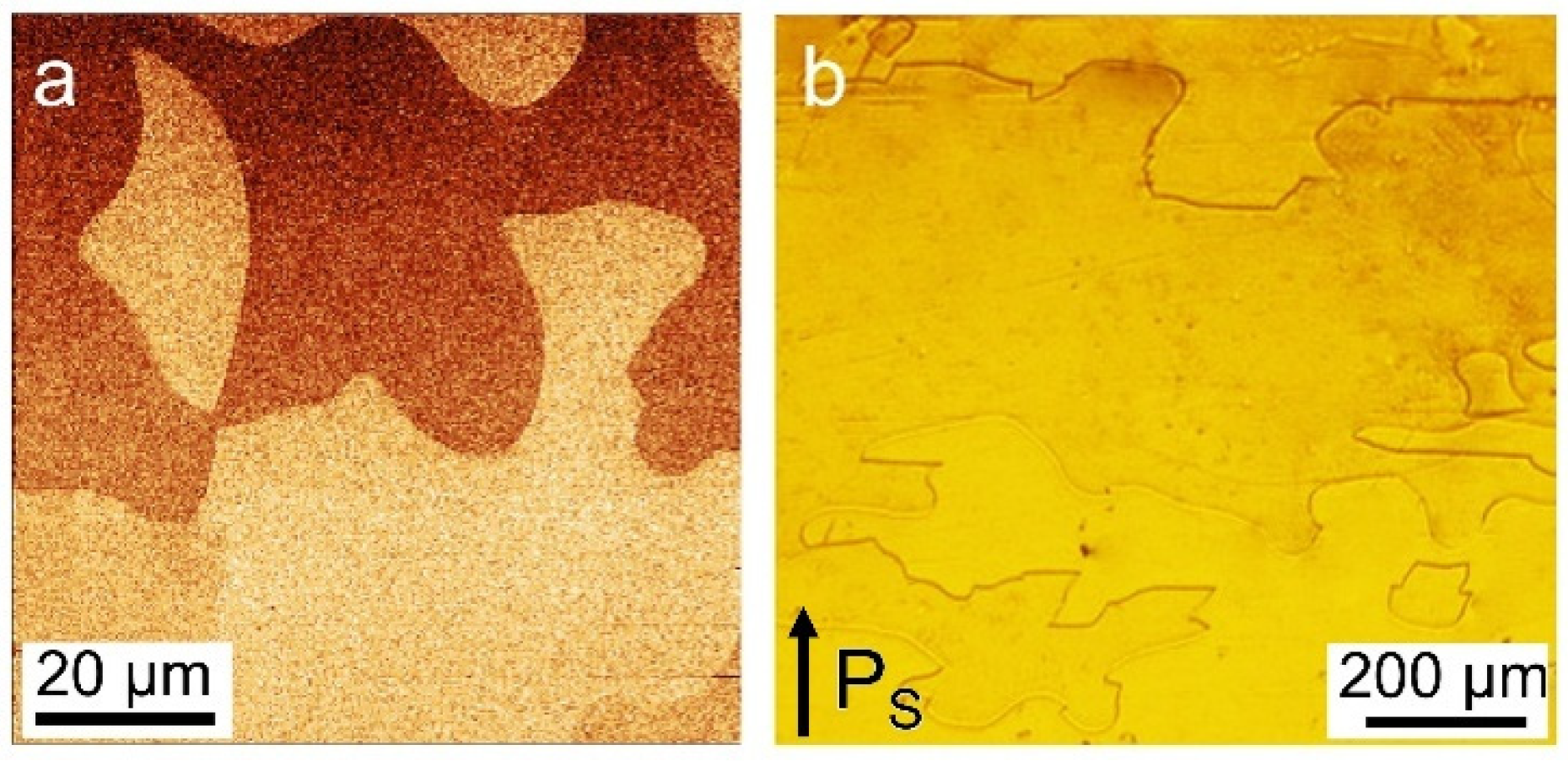
3.1. Initial Domain Structure

The initial domain structure imaged at the polar surface by PFM (Figure 1a) and at the cross-section parallel to the polar direction by optical microscopy after selective etching (Figure 1b) exhibited an irregular shape.
A detailed investigation of the initial domain structure at the cross-section allowed us to reveal the fragments of the almost flat CDWs oriented mostly perpendicular to the polar axis (Figure 1b). It is necessary to point out that such CDWs have never been observed in CVO crystals that were not subjected to annealing in a calcium rich atmosphere [9]. The domain imaging by SHGM confirms the existence of the local fragments of almost flat CDW localized in the bulk (Figure 2c). The SHGM spatial resolution limits detection of submicron domain ledges and the fine structure of CDWs.

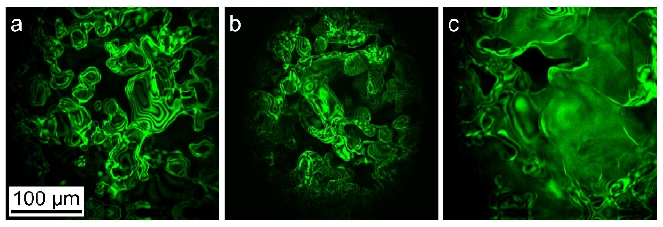
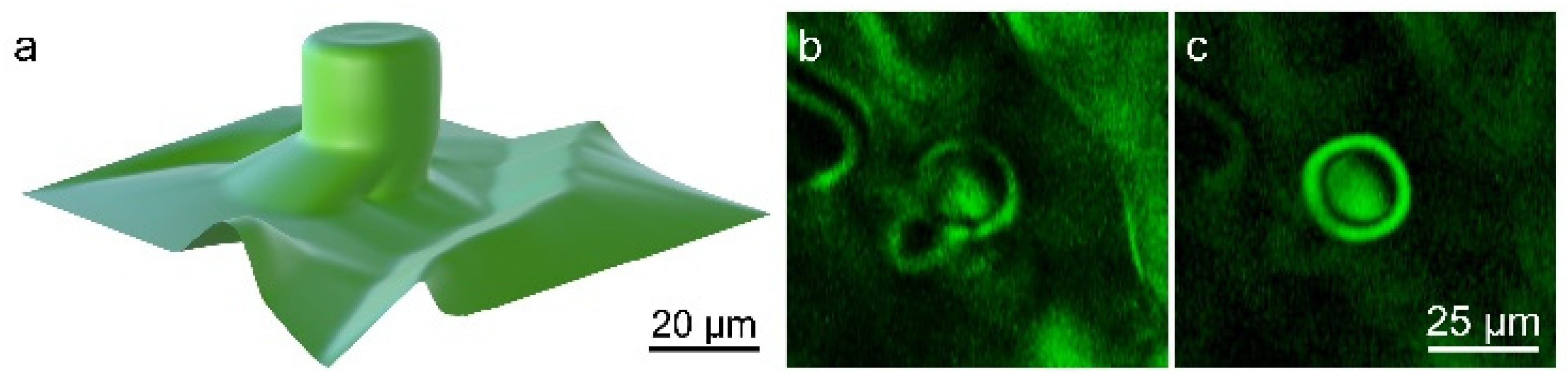
3.2. Switching in the Uniform Field
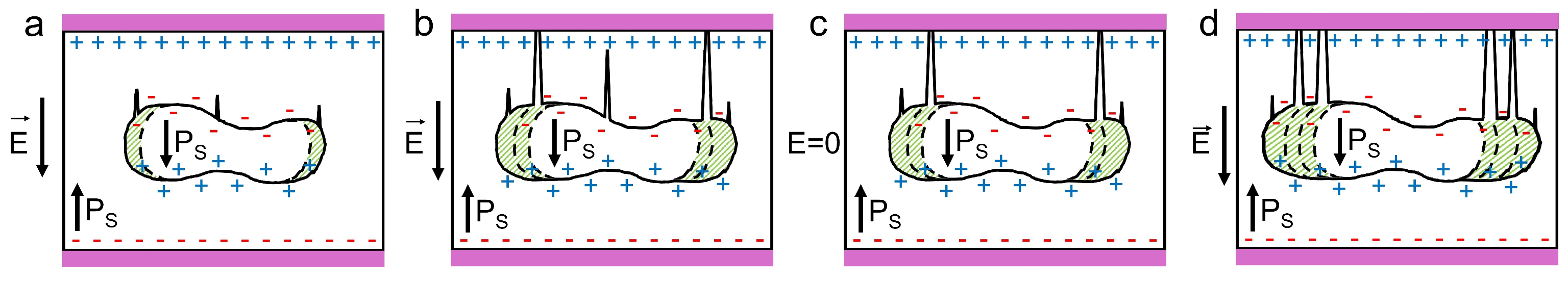
The domain structure evolution obtained during switching by field pulses can be considered as a result of four different scenarios: (1) appearance and disappearance of unstable small isolated domains, (2) sideways growth of large domains in the bulk, (3) appearance of stable small isolated domains at the polar surface, (4) domain growth at the surface by sideways wall motion.
(1) The unstable small isolated domains appeared at the surface during application of the electric field as a result of conical ledge growth from the CDWs of initial in-bulk domains (Figure 3a–d). These domains disappeared completely after field switch-off (Figure 3e). It has been demonstrated previously that rarely when the tip of a growing conical ledge with CDW touches the polar surface does a high value of the conductivity current along the wall result in local degradation, leading to formation of a hole in the electrode [12].
(2) The growth of the initial large in-bulk domains was observed in the vicinity of the electrode edge. It represents the irreversible enlarging by CDW sideways motion perpendicular to the polar direction (Figure 4). The boundary of the switched volume was shifted with a velocity of about 2 μm/s (Eex = 2.5 kV/mm, T = 350 °C). This process leads to the formation of the area with partially screened “fresh CDW” due to the retardation of the bulk screening.
(3) The stable small isolated domains appeared above the fresh CDW (Figure 4) and remained after external electric field switch-off. The domain amount increased with the pulse number (Figure 4). The typical diameters of isolated domains were up to 5 μm.
(4) The stable small domains that appeared at the polar surface above the fresh CDW continued to grow during application of the following field pulses (Figure 5). The large domain appeared at the surface as a result of merging of three small isolated stable domains.
The anisotropic domain growth by sideways motion of the domain wall leads to a shape change. The acquired hexagonal shape of the growing domain is caused by the R3c symmetry of CVO [2].
The essential decrease in the spontaneous backswitching effect in the annealed sample allowed us for the first time obtain the SHGM 3D image of the stable ledge grown from the flat CDW located within the bulk (Figure 6). It is seen that the upper wall of the imaged ledge was almost flat and charged, while the side domain walls were almost parallel to the polar axis and neutral.

4. Discussion

It is known that the walls of the domains that appear in the crystal after ferroelectric phase transition and completely localized in the crystal bulk are mostly charged [19,20,21]. The shape of CDWs is determined by the spatial distribution of the bulk defects and the local deviations from the stoichiometric composition [22,23,24,25]. The local orientation of the spontaneous polarization is defined by the local direction of the defect and deviation gradients. The depolarization field (Edep) produced by bound charges located at the CDW is compensated by the screening field (Escr), which appeared as a result of charge redistribution in the crystal bulk [26]. The high bulk conductivity in CVO existing just below the ferroelectric phase transition temperature led to complete screening of Edep. The subsequent cooling led to the appearance of the pyroelectric field (Epyr) caused by the retardation of the screening process. It was shown in lithium niobate and lithium tantalate that the pyroelectric field can change the shape of CDWs by the formation and growth of the conical ledges [27]. The observed smooth shape of CDWs in CVO (Figure 2) is evidence of the realization of the following CDW stability condition during crystal cooling due to high bulk conductivity of the crystal:
Epyr (T, dT/dt) = Edep (T) − Escr (T,t) < Eth.l. (T)
where Eth.l. is the threshold field value for ledge appearance.
Thus, the initial domain structure in CVO consisted of the irregular-shaped domains with smoothed CDWs and almost completely screened Edep. The local surface density of the bound charges (σ) at CDW depended on the local value of the wall deviation from the polar direction [9].
σ (α) = 2 Ps sin (α)
where α is the local angle between the polar axis and normal to CDW.
This dependence led to nonuniform spatial distribution of the bound charges and appropriate screening charges at the walls of any domain completely located in the crystal bulk.
After application of the external electric field, the sideways wall motion is obtained only if the value of the polar component of the spatially nonuniform local field (Eloc.z) is above the threshold for step generation (Eth.s.) at CDW
Eloc.z = Eex + Edep.z − Escr.z (t) = Eex + Erd.z > Eth.s
where Erd.z is the polar component of the residual depolarization field that appeared as a result of screening retardation.
The growth of the initial large domains in the crystal bulk was caused by generation of the elementary steps at the domain edge possessing the lowest density of the bound charges and according to the lowest value of the screening charge (Figure 7a). The depolarization field that appeared after wall shift was proportional to the screening charge value. This field obstructed the wall shift and therefore the low screening charge at the domain edge led to a wall shift mostly in the direction normal to the polar axis.
The partial screening of the fresh CDW was due to retardation of the screening process, thus facilitating the appearance of the ledges (Figure 7a). The ledges grew in the external field and became stable after touching the polar surface.
The rare appearance of the ledges far from the CDW edge can be attributed to the local decreases of the threshold field value stimulated by bulk defects. The bound charge of these ledges was essentially larger than that which appeared at the edge of the fresh CDW.
The ledge growth in the polar direction was slowed down in the vicinity of the polar surface due to the existence of the dielectric gap and spatial distribution of the screening charge [28]. This effect is more pronounced for large charges and results in growth interrupting at the distance about screening length from the polar surface of the ledges that appeared far from the CDW edge. Thus, the ledges that appeared at the fresh CDW edge grew out to the polar surface and became stable due to effective external screening. In contrast, the ledges that appeared far from CDW edge were unstable and backswitched completely after external field switch-off (Figure 7c).
Finally, we were able to distinguish the four main stages of the domain structure evolution under the application of the field pulses.
First, after field switch-on, the sideways motion of the CDW located in the bulk led to the formation of the fresh CDW and appearance of the ledges (Figure 7a).
Second, the ledges appeared at the edges of the fresh CDW growing in the external field until touching the polar surface. In contrast, the rare ledges that appeared far from the CDW edge interrupted their growth in the vicinity of the polar surface (Figure 7b).
Third, the field switch-off led to the complete backswitching of the unstable ledges that appeared far from CDW edge (Figure 7c).
Fourth, after the subsequent field switch-on, the stable domains that appeared at the surface above the fresh CDW continued to grow (Figure 7d).
For statistical characterization of the domain formation and growth on the polar surface, we used the dependence of the fresh CDW area on the pulse number (Figure 8a). The obtained linear dependence with small deviations caused by bulk defects allowed us to reveal that the sideways domain wall motion velocity was about 2 μm/s for Eex = 2.5 kV/mm, T = 350 °C.
It was shown that the ledge appearance started with pronounced delay time after the application of three pulses with a total duration of about 9 s (Figure 8b). The obtained delay time can be attributed to a time interval, which is necessary for the formation of a large enough shift of the fresh CDW for ledge appearance. The rate of the ledge appearance was about 3.3 ± 0.2 s−1.
The linear dependence of the total ledge number on the fresh CDW area allowed us to reveal that the ledge appeared only in the narrow band close to the edge of the fresh CDWs (Figure 8c).
The finite element method by means of a COMSOL Multiphysics 5.2 software package was used to calculate the spatial distribution of the polar component of the residual depolarization field Erd.z in the vicinity of the model elliptically shaped domain located in the crystal bulk. A two-dimensional simulation approach with second-order finite elements for stationary Gauss law was performed. The size of the elements near the domain boundary was 3.5 nm and expanded to 2 μm when approaching the model boundary. The model domain was simulated as an ellipse with a semi-axis of 5 µm and 1 µm with minor-axe oriented along the polar direction. The spatial distribution of the bound charge at the domain wall was calculated according to Equation (2). The external boundary conditions represent grounding by a layer of grounded infinite elements. In order to validate the computational results, a grid convergence study was carried out to make the results robust to element size and external boundary conditions.
We calculated the situation when the screening charges were located at the distance h = 10 nm from the bound charges as a result CDW shift in an external electric field (Figure 9a). It was demonstrated that the maximum of Erd.z was situated in the vicinity of the domain edges (Figure 9b,c). Such field distribution defines the experimentally obtained positions of the ledge appearance at some distance from the boundary of a growing large in-bulk domain.

5. Conclusions

The field-induced evolution of an as-grown domain structure was studied in an annealed calcium orthovanadate (CVO) crystal under the application of the series of electric field pulses at elevated temperature using various in situ and ex situ methods of domain imaging. It was shown that the evolution of domain structure with charged domain walls (CDW) in the bulk under the action of the electric field represented the sideways growth of initial large domains located in the bulk and the appearance of unstable and stable isolated domains at the polar surface. The sideways domain growth in the bulk was caused by the lowest density of the bound and screening charges at the domain edges, which facilitated the CDW shift in the direction perpendicular to the polar axis. The screening retardation of the fresh CDW facilitated the appearance of the ledges, which grew in the external field and became stable after touching the polar surface. Thus, after field switch-on, the CDW shift in the bulk by sideways motion led to the formation of the fresh CDW and the ledge appearance at its edges in the residual depolarization field and growth in the external field until it touched the polar surface. The rare ledges that appeared far from the CDW edge interrupted their growth in the vicinity of the polar surface and backswitched completely after the field switch-off. The stable domains continued to grow at the surface after subsequent field switch-on. The obtained domain structure evolution was considered in terms of the kinetic approach. The finite element method by means of a COMSOL Multiphysics software package was used to calculate the spatial distribution of the polar component of the residual depolarization field in the vicinity of the domain with CDW located in the crystal bulk. The demonstrated facilitating of the domain switching in CVO as a result of crystal annealing in a calcium-rich atmosphere can be attributed to compositional changes and homogenization. The results obtained show the way to create the periodic domain structure in CVO by the sample pretreatment and choosing the optimal parameters of electric field application.

Author Contributions

Conceptualization, V.S., E.S. and A.A.; methodology, E.S.; software, E.L., M.K. and S.M.; investigation, V.Y. and M.C.; resources, L.I. and A.T.; writing—original draft preparation, E.S. and V.S.; writing—review and editing, V.S. and E.P.; visualization, M.N., V.Y. and M.C.; supervision, V.S.; project administration, V.S. All authors have read and agreed to the published version of the manuscript.

Funding

The authors are grateful for financial support of the Ministry of Science and Higher Education of the Russian Federation (state task FEUZ-2023-0017).

Data Availability Statement

The data presented in this study are available on request from the corresponding author.

Acknowledgments

The equipment of the Ural Center for Shared Use “Modern nanotechnology” Ural Federal University (reg. No. 2968) was used.

Conflicts of Interest

The authors declare no conflicts of interest.

References

  1. Brixner, L.H.; Flournoy, P.A. Calcium orthovanadate Ca3(VO4)2-a new laser host crystal. J. Electrochem. Soc. 1965, 112, 303–308. [Google Scholar] [CrossRef]
  2. Glass, A.M.; Abrahams, S.C.; Ballman, A.A.; Loiacono, G. Calcium orthovanadate, Ca3(VO4)2-a new high-temperature ferroelectric. Ferroelectrics 1977, 17, 579–582. [Google Scholar] [CrossRef]
  3. Bechthold, P.S.; Liebertz, J.; Deserno, U. Linear and nonlinear optical properties of Ca3(VO4)2. Opt. Commun. 1978, 27, 393–398. [Google Scholar] [CrossRef]
  4. Ivleva, L.I.; Dunaeva, E.E.; Voronina, I.S.; Doroshenko, M.E.; Papashvili, A.G. Ca3(VO4)2:Tm3+—A new crystalline medium for 2-μm lasers. J. Cryst. Growth 2018, 501, 18–21. [Google Scholar] [CrossRef]
  5. Hum, D.S.; Fejer, M.M. Quasi-phasematching. Comptes Rendus Phys. 2007, 8, 180–198. [Google Scholar] [CrossRef]
  6. Fejer, M.M.; Jundt, D.H.; Byer, R.L.; Magel, G.A. Quasi-phase-matched second harmonic generation: Tuning and tolerances. IEEE J. Quantum Electron. 1992, 28, 2631–2654. [Google Scholar] [CrossRef]
  7. Byer, R.L. Quasi-phasematched nonlinear interactions and devices. J. Nonlinear Opt. Phys. Mater. 1997, 6, 549–592. [Google Scholar] [CrossRef]
  8. Shishkina, E.V.; Greshnyakov, E.D.; Zelenovskiy, P.S.; Yuzhakov, V.V.; Ivleva, L.I.; Shur, V.Y. Micro-Raman domain imaging in calcium orthovanadate single crystals. Ferroelectrics 2021, 576, 85–93. [Google Scholar] [CrossRef]
  9. Shishkina, E.; Yuzhakov, V.; Nebogatikov, M.; Pelegova, E.; Linker, E.; Ivleva, L.; Shur, V. As-grown domain structure in calcium orthovanadate crystals. Crystals 2021, 11, 1508. [Google Scholar] [CrossRef]
  10. Sheng, Y.; Best, A.; Butt, H.J.; Krolikowski, W.; Arie, A.; Koynov, K. Three-dimensional ferroelectric domain visualization by Čerenkov-type second harmonic generation. Opt. Express 2010, 18, 16539–16545. [Google Scholar] [CrossRef]
  11. Shishkina, E.V.; Chuvakova, M.A.; Yuzhakov, V.V.; Akhmatkhanov, A.R.; Pelegova, E.V.; Nebogatikov, M.S.; Ushakov, A.D.; Linker, E.A.; Ivleva, L.I.; Shur, V.Y. Domain structure evolution during polarization reversal in calcium orthovanadate single crystals. J. Appl. Phys. 2022, 132, 184101. [Google Scholar]
  12. Yuzhakov, V.V.; Chuvakova, M.A.; Shishkina, E.V.; Nebogatikov, M.S.; Linker, E.A.; Akhmatkhanov, A.R.; Pelegova, E.V.; Ivleva, L.I.; Shur, V.Y. Kinetics of the domain structure in calcium orthovanadate crystals under application of the series of electric field pulses. Ferroelectrics 2024, 618, 1339–1345. [Google Scholar]
  13. Doshi, S.P.; West, G.N.; Gray, D.; Ram, R.J. Thermal enhancement of defect motion for optimizing periodic poling of X-cut thin-film lithium niobate. Appl. Phys. Lett. 2024, 125, 261103. [Google Scholar]
  14. Gopalan, V.; Gupta, M.C. Observation of internal field in LiTaO3 single crystals: Its origin and time-temperature dependence. Appl. Phys. Lett. 1996, 68, 888–890. [Google Scholar]
  15. Holman, R.L.; Cressman, P.J.; Revelli, J.F. Chemical control of optical damage in lithium niobate. Appl. Phys. Lett. 1978, 32, 280–283. [Google Scholar] [CrossRef]
  16. Gonzalez, M.; Margueron, S.; Murauskas, T.; Boulet, P.; Gauthier-Manuel, L.; Dulmet, B.; Bartasyte, A. Influence of parameters in vapor transport equilibration treatment on composition and homogeneity of LiTaO3 single crystals. Phys. Status Solidi 2025, 222, 2400129. [Google Scholar]
  17. Bordui, P.F.; Norwood, R.G.; Jundt, D.H.; Fejer, M.M. Preparation and characterization of off-congruent lithium niobate crystals. J. Appl. Phys. 1992, 71, 875–879. [Google Scholar]
  18. Kämpfe, T.; Reichenbach, P.; Haußmann, A.; Woike, T.; Soergel, E.; Eng, L.M. Real-time three-dimensional profiling of ferroelectric domain walls. Appl. Phys. Lett. 2015, 107, 152905. [Google Scholar]
  19. Gureev, M.Y.; Mokrý, P.; Tagantsev, A.K.; Setter, N. Ferroelectric charged domain walls in an applied electric field. Phys. Rev. B Condens. Matter Mater. Phys. 2012, 86, 104104. [Google Scholar]
  20. Gureev, M.Y.; Tagantsev, A.K.; Setter, N. Head-to-head and tail-to-tail 180° domain walls in an isolated ferroelectric. Phys. Rev. B 2011, 83, 184104. [Google Scholar]
  21. Tagantsev, A.K.; Cross, L.E.; Fousek, J. Domains in Ferroic Crystals and Thin Films; Springer: New York, NY, USA, 2010. [Google Scholar]
  22. Morozovska, A.N.; Eliseev, E.A.; Svechnikov, G.S.; Kalinin, S.V. Mesoscopic mechanism of the domain wall interaction with elastic defects in uniaxial ferroelectrics. J. Appl. Phys. 2013, 113, 187203. [Google Scholar]
  23. Gopalan, V.; Dierolf, V.; Scrymgeour, D.A. Defect-domain wall interactions in trigonal ferroelectrics. Annu. Rev. Mater. Res. 2007, 37, 449–489. [Google Scholar]
  24. Yang, T.J.; Gopalan, V.; Swart, P.J.; Mohideen, U. Direct observation of pinning and bowing of a single ferroelectric domain wall. Phys. Rev. Lett. 1999, 82, 4106–4109. [Google Scholar]
  25. Robels, U.; Arlt, G. Domain wall clamping in ferroelectrics by orientation of defects. J. Appl. Phys. 1993, 73, 3454–3460. [Google Scholar]
  26. Shur, V.Y.; Pelegova, E.V.; Turygin, A.P.; Kosobokov, M.S.; Alikin, Y.M. Forward growth of ferroelectric domains with charged domain walls. local switching on non-polar cuts. J. Appl. Phys. 2021, 129, 044103. [Google Scholar]
  27. Greshnyakov, E.; Chuvakova, M.; Ushakov, A.; Akhmatkhanov, A.; Kosobokov, M.; Pryakhina, V.; Shur, V. In-bulk polarization reversal in lithium tantalate with single charged domain wall. J. Adv. Dielectr. 2023, 14, 2350032. [Google Scholar]
  28. Morozovska, A.N.; Eliseev, E.A.; Svechnikov, S.V.; Krutov, A.D.; Shur, V.Y.; Borisevich, A.Y.; Maksymovych, P.; Kalinin, S.V. Finite size and intrinsic field effect on the polar-active properties of ferroelectric-semiconductor heterostructures. Phys. Rev. B 2010, 81, 205308. [Google Scholar]
Figure 1. The images of the initial domain structure: (a) at the polar surface by PFM; (b) at the cross-section parallel to the polar axis by optical microscopy after selective etching.
Crystals 15 00315 g001
Figure 2. SHGM domain images of the same region (a) near the polar surface and at different depth: (b) 100 µm, (c) 200 µm.
Crystals 15 00315 g002
Figure 3. The appearance of the small isolated unstable domains at the polar surface vanished after pulse termination under the application of the third pulse. Images (ad) correspond to different time interval from start of the pulse, (e) after end of the pulse. In situ imaging by optical microscopy. The holes in the electrode are marked in green. Eex = 2.5 kV/mm, T = 350 °C.
Crystals 15 00315 g003
Figure 4. The optical images of the large domain growth by sideways wall motion in the bulk from the edge of the electrode and appearance of the stable small isolated domains above the fresh CDW. Images (ac) correspond to domain structure after proper number of pulses. Domain boundary is marked in blue, and the electrode edge in violet. Eex = 2.5 kV/mm, T = 350 °C.
Crystals 15 00315 g004
Figure 5. The growth and shape change of the stable domain at the polar surface above the fresh CDW. Images (ac) correspond to domain structure after proper number of pulses. Optical microscopy. Eex = 2.5 kV/mm, T = 350 °C.
Crystals 15 00315 g005
Figure 6. SHG imaging at different depths of the ledge grown from CDW. (a) three-dimensional image and two-dimensional images: (b) ledge bottom at 180 µm depth and (c) ledge top at 200 µm depth.
Crystals 15 00315 g006
Figure 7. The scheme of the main stages of domain structure evolution: (a) formation of the fresh CDW and ledges in the field, (b) growing out of the ledges appeared at the edges of the fresh CDW and growing interruption of the ledges that appeared far from CDW edge, (c) complete backswitching of the unstable ledges appeared far from the CDW edge after field switch-off, (d) growth of the stable domains at the polar surface in the field.
Crystals 15 00315 g007
Figure 8. (a) Dependence of the fresh CDW area on pulse number. Dependences of the number of the ledges formed on the fresh CDW: (b) on pulse number and (c) on fresh CDW area. Statistics collected from the area are presented in Figure 4. Eex = 2.5 kV/mm, T = 350 °C.
Crystals 15 00315 g008
Figure 9. The simulated spatial distribution of the polar component of the residual depolarization field Erd.z in the vicinity of the screened elliptically shaped domain located in the crystal bulk. (a) Scheme of the simulated domain with screening charges shifted from the bound ones under the application of the external field. Calculated 2D distribution of Erd.z: (b) common view and (c) enlarged region.
Crystals 15 00315 g009
Disclaimer/Publisher’s Note: The statements, opinions and data contained in all publications are solely those of the individual author(s) and contributor(s) and not of MDPI and/or the editor(s). MDPI and/or the editor(s) disclaim responsibility for any injury to people or property resulting from any ideas, methods, instructions or products referred to in the content.

