Article

Biphasic WO3 Nanostructures via Controlled Crystallization: Achieving High-Performance Electrochromism Through Amorphous/Crystalline Heterointerface Design

1
Key Laboratory of Architectural Cold Climate Energy Management, Ministry of Education, Jilin Jianzhu University, Changchun 130118, China
2
School of Electrical and Computer Science, Jilin Jianzhu University, Changchun 130118, China
3
Department of Chemistry, Jilin Normal University, Siping 136000, China
*
Authors to whom correspondence should be addressed.
Crystals 2025, 15(4), 324; https://doi.org/10.3390/cryst15040324
Submission received: 10 March 2025 / Revised: 26 March 2025 / Accepted: 26 March 2025 / Published: 28 March 2025

Abstract

:
WO3 electrochromic films have emerged as potential candidates for smart windows due to their cost-effectiveness, fast switching speed, and strong chemical stability. However, the inherent contradiction between the high coloring efficiency of amorphous WO3 and the cycling durability of crystalline WO3 remains a critical challenge in practical applications. This study proposes an innovative heterostructure engineering strategy, achieving precise control of the amorphous/crystalline bilayer WO3 heterointerface (148 nm a-WO3/115 nm c-WO3) for the first time through phase boundary regulation, using well-controlled magnetron sputtering and post-deposition thermal annealing processes. Multimodal characterization using XRD, XPS, and SEM indicates that the heterointerface optimizes performance through a dynamic charge transfer mechanism and structural synergistic effects: the optimized bilayer structure achieves 76.57% optical modulation (at 630 nm) under −1.0 V and maintains a ΔT retention rate of 45.02% after 600 cycles, significantly outperforming single amorphous (8.34%) and crystalline films (14.34%). XPS analysis reveals a dynamic equilibrium mechanism involving W5+/Li+ at the interface, and the Li+ diffusion coefficient (D0 = 4.29 × 10⁻¹⁰ cm2/s) confirms that the amorphous layer dominates rapid ion transport, while the crystalline matrix enhances structural stability through its ordered crystalline structure. This study offers a new paradigm for balancing the efficiency and longevity of electrochromic devices, with the compatibility of magnetic sputtering promoting the industrialization process of large-area smart windows.

1. Introduction

The global energy security faces unprecedented challenges under accelerating urbanization and climate change pressures, where building operations account for 30–40% of total energy consumption primarily attributed to thermal regulation and artificial lighting systems [1,2]. Electrochromic smart windows emerge as a disruptive energy-saving technology capable of dynamically modulating solar irradiation through reversible optical switching, demonstrating immense potential to reduce 20–30% of building HVAC (Heating, Ventilation, and Air Conditioning) energy demand [3]. Among various electrochromic candidates like WO3 [4], V2O5 [5], TiO2 [6], MoO3 [7], and NiO [8], WO3 has garnered particular attention due to its exceptional coloration efficiency (>50 cm2/C) and sub-5-s switching kinetics [9,10]. The metastable amorphous WO3 phase dominates room-temperature synthesized films, offering superior Li+ diffusion channels for rapid electrochromic responses [11,12]. However, its disordered atomic arrangement inevitably induces deep ion trapping during prolonged cycling, leading to irreversible capacity decay (>40% after 2000 cycles) [13]. Conversely, crystalline WO3 phases (monoclinic/tetragonal) exhibit enhanced structural stability but suffer from sluggish ion transport kinetics due to restrictive crystalline lattice pathways [14].
As highlighted by Granqvist [12], phase-boundary engineering through amorphous/crystalline heterointerfaces has emerged as a key strategy to synergistically combine the merits of both phases, balancing ion mobility and structural integrity. Zhou [15] demonstrated crystalline-amorphous core-shell WO3 nanowires achieving 70.3% optical modulation at 730 nm with 10,000-cycle durability, while Huo’s team [16] developed hexagonal WO3 nanorods with 4 nm amorphous shells showing record coloration efficiency (101 cm2/C at 800 nm). These breakthroughs underscore the critical role of interfacial phase compatibility in balancing ion mobility and structural integrity. Nevertheless, such solution-processed architectures relying on hydrothermal/electrodeposition methods face inherent scalability limitations, including low deposition rates and substrate size constraints, hindering industrial adoption [17].
Herein, we propose a scalable phase-boundary modulation strategy using industrially compatible magnetron sputtering combined with precision thermal annealing [18]. By spatially decoupling amorphous and crystalline WO3 layers through deposition parameter control, we fabricate bilayer architectures. This design leverages the high Li+ diffusivity of amorphous matrices while utilizing crystalline frameworks as structural stabilizers. This work establishes a paradigm for designing phase-engineered electrochromic systems compatible with roll-to-roll manufacturing processes.

2. Experiment

2.1. Preparation of Phase-Engineered Bilayer WO3 Thin Films

Indium tin oxide (ITO)-coated glass substrates (1.0 × 2.0 cm2, sheet resistance: 7–10 Ω/sq) underwent sequential ultrasonic cleaning in acetone, anhydrous ethanol, and deionized water for 10 min per solvent. Residual contaminants were removed via high-purity nitrogen blow-drying under laminar flow conditions. Amorphous WO3 (a-WO3) layers were deposited using a QMS-450 RF magnetron sputtering system (Weikemu General Instruments Co., Shenyang, China) equipped with a 50 mm diameter × 5 mm thickness WO3 target (99.99% purity). The magnetron sputtering process was conducted under ambient temperature conditions, utilizing a sputtering power of 100 W (corresponding to a power density of 4.0 W/cm2). The deposition was carried out in a controlled Ar/O2 atmosphere with a gas flow ratio of 90:10, while maintaining a constant chamber pressure of 1.4 Pa throughout the process.
The as-deposited amorphous WO3 (a-WO3) films underwent crystallization in a horizontal tube furnace (OTF-1200X, Kejing Materials Technology Co., Hefei, China) under ambient atmospheric conditions. A controlled thermal annealing process was implemented at 400 °C for 2 h in air atmosphere, resulting in the formation of crystalline WO3 (c-WO3) films with enhanced structural stability.
A sequential two-step sputtering strategy was developed to fabricate amorphous/crystalline (a/c) WO3 heterostructures with precisely controlled phase boundaries as shown in Figure 1. The fabrication protocol comprised the following: (1) crystalline base layer formation—initial 15 min sputtering followed by thermal annealing to create a fully crystallized c-WO3 layer; (2) amorphous top layer deposition—secondary sputtering with varying durations (10/30/50 min) to generate a-WO3 layers with controlled thickness. The resulting samples were systematically labeled as: 0 min–15 min (c-WO3 (15 min)/ITO), and 10 min–15 min, 30 min–15 min, 50 min–15 min (heterostructures: a-WO3 (10/30/50 min)/c-WO3 (15 min)/ITO), and 0 min–30 min (a-WO3 (30 min)/ITO).

2.2. Structural and Electrochemical Characterization

The crystal structure of the thin was characterized by XRD (Rigaku D/max-2500V/PC X-ray diffractometer, Tokyo, Japan). The surface morphology and cross-sectional features of the films were examined by a JSM-7610F scanning electron microscope (SEM, JEOL Ltd., Tokyo, Japan). Optical properties were measured by a UV-2600 UV-visible spectrophotometer (Shimadzu Corpo-ration, Kyoto, Japan). The electrochemical properties of the electrochromic thin films were evaluated using a CHI760E electrochemical workstation (Shanghai Chenhua Instrument Co., Ltd., Shanghai China), which employs a conventional three-electrode system: a platinum foil as the counter electrode, Ag/AgCl as the reference electrode, and the prepared film as the working electrode. The electrolyte was 1 mol/L lithium perchlorate dissolved in propylene carbonate (LiClO4/PC, Kolod New Energy Technology Co., Ltd., Dongguan, China). Cyclic voltammetry (CV) was performed using an electrochemical workstation and a conventional three-electrode configuration, and the cyclic voltammetry curves were tested for different cycling rates (0.01 V/s~0.10 V/s) in the range of −1 V~+1 V. The cyclic stability of the films was tested using the chronoamperometry (CA) method, with the test voltage of ±1 V and the pulse width of 20 s. The cyclic voltammetry profiles before and after cycling were finally compared with those before and after the sweeping rate of 0.05 V/s cyclic voltammetry before and after cycling. As for testing the transmittance under coloring and fading condition, this was performed by the amperage-time curve (i-t) method by applying a constant voltage (−0.8 V~−1.4 V) for about 5 min, so that it was fully colored and then the transmittance of the films at 300~800 nm was tested by UV spectrophotometer.
XPS tests were performed using a Thermo Fisher Scientific X-ray photoelectron spectrometer equipped with a monochromatic Al Kα x-ray source (1486.6 eV) (Thermo Fisher Scientific ESCALAB 250Xi system, Waltham, MA, USA). High-resolution spectra were acquired with a 500 µm spot size and 30 eV pass energy. The charge neutralization was monitored using the C 1s (284.8 eV) signal for adventitious carbon. Prior to measurements, all samples were electrochemically colored by applying −1 V for 5 min using an electrochemical workstation. To minimize surface contamination and oxidation state changes, the colored films were blown dry using a dust-free cloth and nitrogen gun to remove the residual liquid on the surface, and then put into the XPS chamber to evacuate in the shortest possible time.

3. Results and Discussion

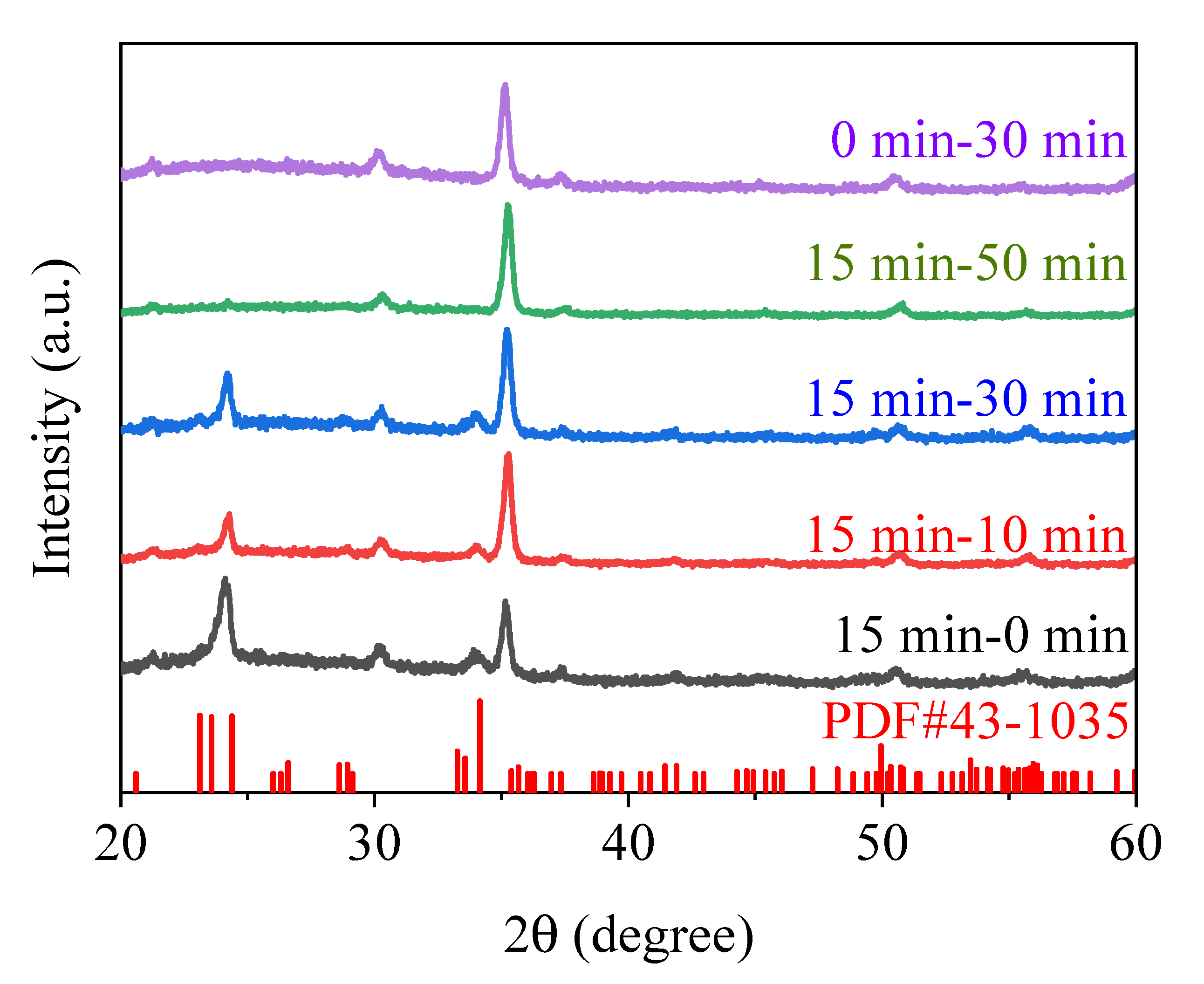
3.1. Structural Characterization of Phase-Engineered Bilayer WO3 Thin Films

The phase evolution of WO3 films was investigated using X-ray diffraction (XRD). As shown in Figure 2, the as-deposited amorphous WO3 (a-WO3) films exhibit a broad hump characteristic of disordered atomic arrangements. After thermal annealing at 400 °C, distinct diffraction peaks emerge at 23.1°, 24.4°, and 34.2°, corresponding to the (002), (200), and (202) crystallographic planes of monoclinic WO3 (JCPDS 43-1035) [19,20]. This phase transformation confirms the successful crystallization of a-WO3 into a well-defined monoclinic structure, consistent with previous reports on thermally induced WO3 crystallization [21]. The sharpening of diffraction peaks further indicates improved crystallinity and long-range atomic ordering [22].

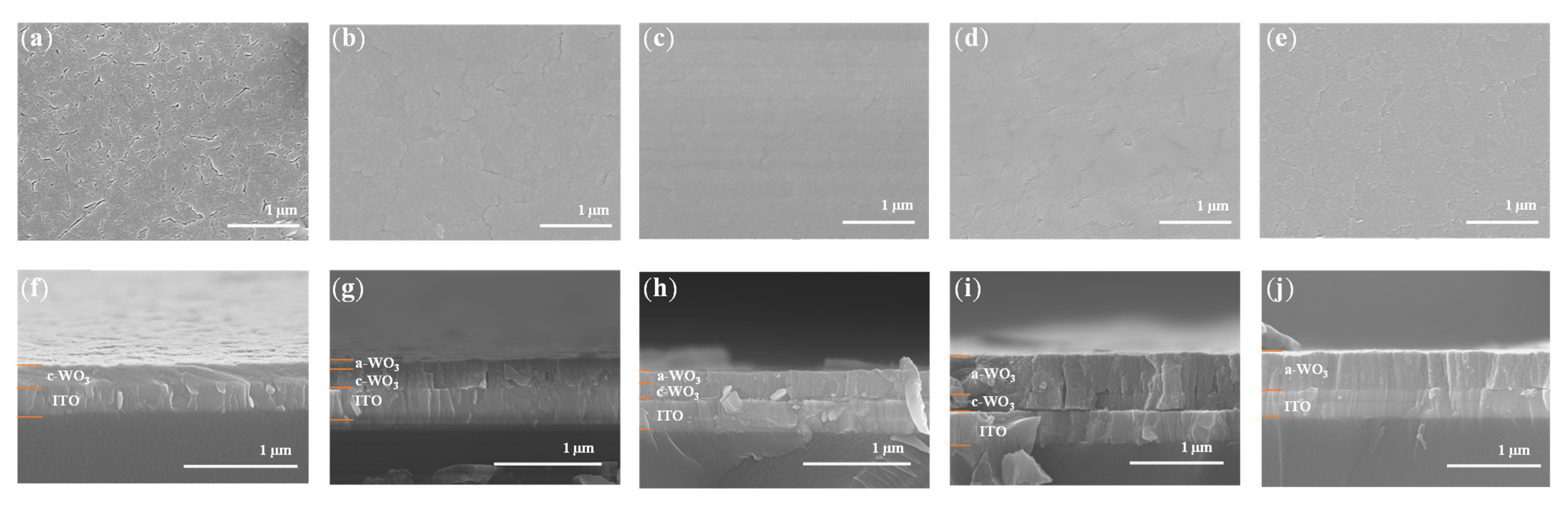
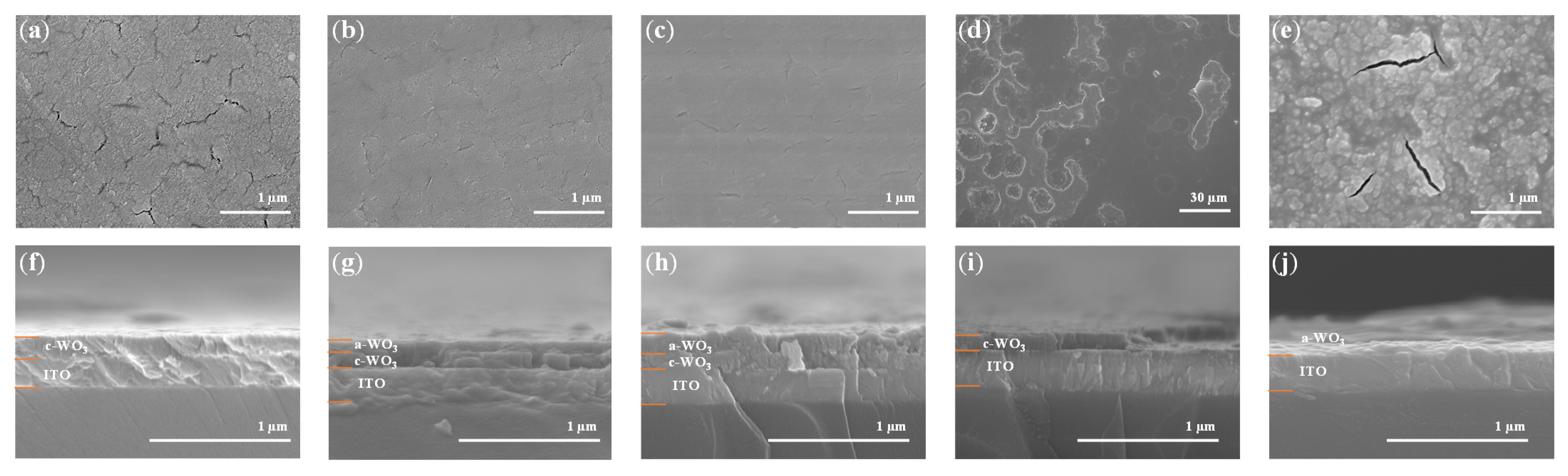
3.2. Morphological and Cross-Sectional Analysis

The surface and cross section morphology of WO3 thin films were characterized by scanning electron microscopy (SEM), as shown in Figure 3a–j. Figure 3a–e is the SEM image of the surface, and there are no obvious voids on other surfaces except Figure 3a (15 min–0 min), where there are more voids. Figure 3f–j is a cross-section image, where each double-layer structure is clearly visible and the thickness of the crystal base (c-WO3) is 115 nm. The thickness of the amorphous top layer (a-WO3) was 73 nm (15 min–10 min), 148 nm (15 min–30 min), and 322 nm (15 min–50 min), respectively. The thickness of the independent a-WO3 film (0 min–30 min) is 262 nm. It is noteworthy that surface roughness systematically decreases with increasing a-WO3 thickness, indicating a smoothing effect during sequential deposition [23]. This morphological evolution is attributed to the filling of the surface void during the secondary sputtering process.

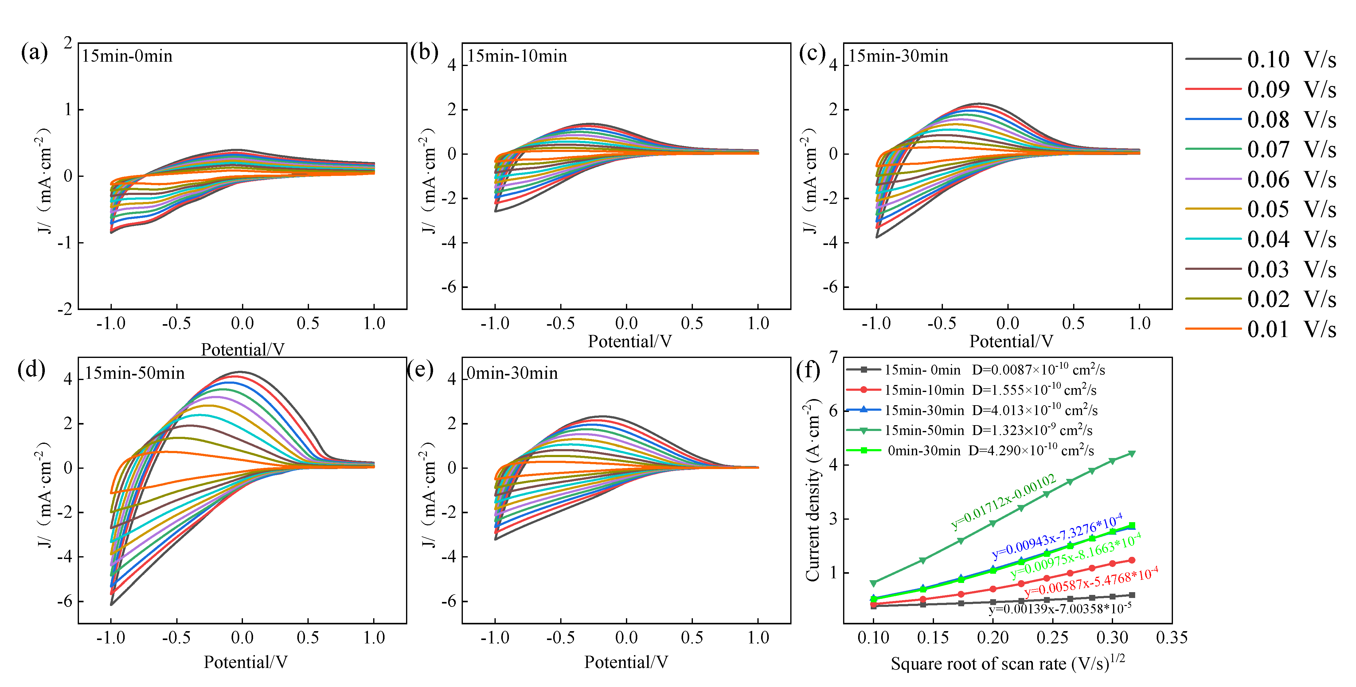
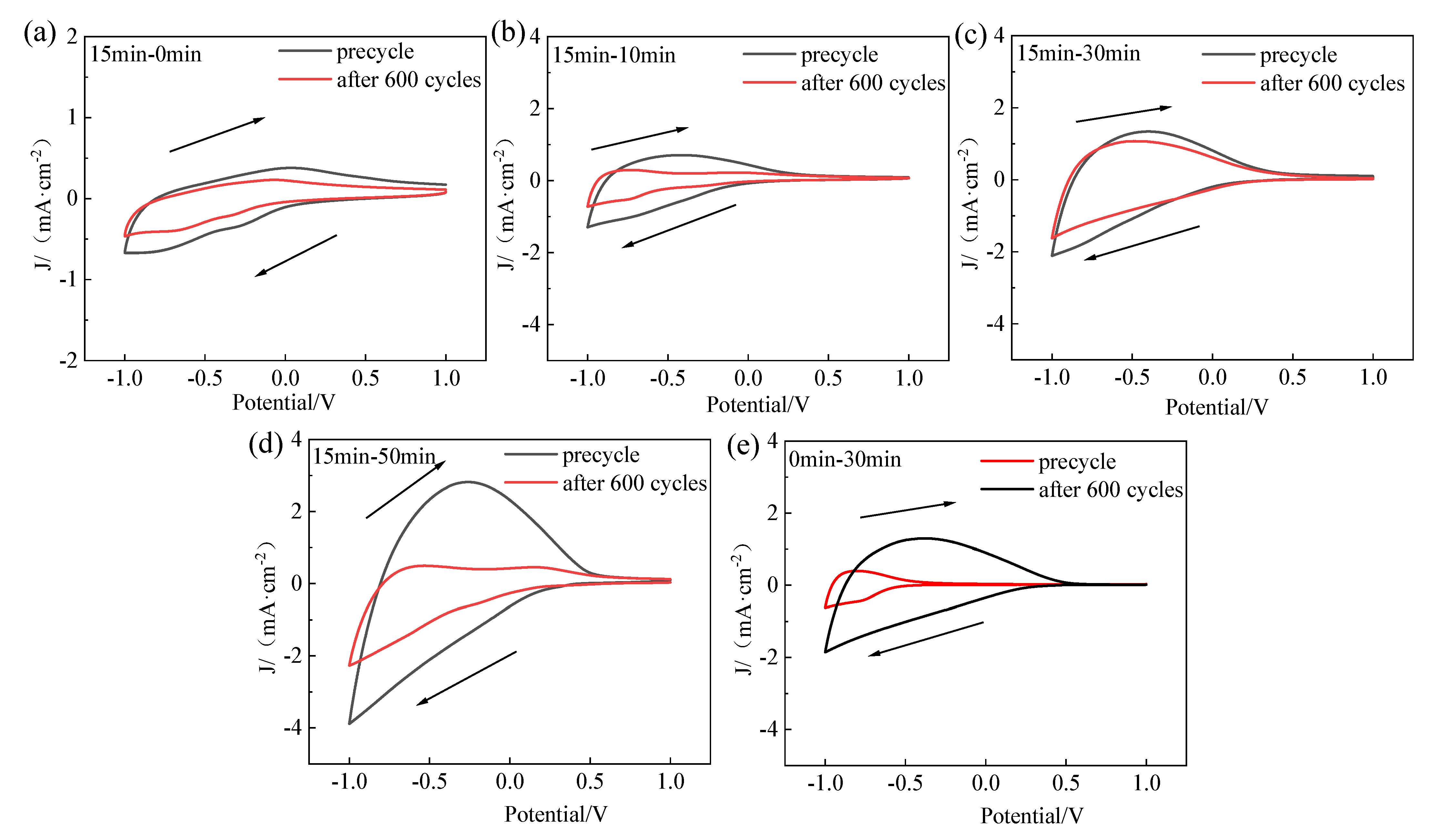
3.3. Electrochromic Performance Evaluation

The electrochemical and electrochromic (EC) performance of WO3 films was evaluated in a three-electrode spectroelectrochemical cell using 1 M PC/LiClO4 as the electrolyte. To intuitively assess the impact of the amorphous/crystalline layer thickness on electrochemical and EC performance, Figure 4a–e compares the cyclic voltammetry (CV) curves at different scan rates. The integrated CV area, which is proportional to the charge storage capacity, monotonically increases with the thickness of the a-WO3 film, confirming the dominant role of the amorphous phase in the ion insertion/extraction process. The higher current density and larger CV area of the WO3 films suggest that the oxygen vacancies within the films can provide more available sites for the insertion/extraction of Li+ [24].
In order to further evaluate the effect of oxygen vacancies on the Li diffusion kinetics in the WO3 host, the lithium diffusion coefficients of the five films were calculated using the Randles–Sevcik equation based on the CV curves measured at different scan rates [25]:
Ip = 2.72 × 10⁵ × n3/2 × A × D01/2 × C0 × v1/2
where Ip is the peak current (A), A is the electrode area (cm2), C0 is the electrolyte concentration (mol/mL), n is the number of electrons transferred (n = 1 for Li+), and v is the scan rate (V/s). The derived D0 values span from 0.0087 × 10⁻¹⁰ cm2/s (15 min–0 min) to 4.290 ×10⁻¹⁰ cm2/s (0 min–30 min), demonstrating a strong correlation with a-WO3 thickness (Figure 4f). This trend underscores the superior ionic conductivity of the amorphous phase compared to its crystalline counterpart, consistent with the open network structure of a-WO3 facilitating rapid ion transport [26]. The long-term durability of the films was evaluated by comparing initial and post-cycling CV profiles after 600 cycles at 0.05 V/s (Figure 5a–e). The bilayer films (15 min–0 min, 15 min–10 min, 15 min–30 min) exhibit exceptional stability, attributed to the structural reinforcement provided by the crystalline base layer. In contrast, the standalone a-WO3 film (0 min–30 min) suffers from severe degradation, likely due to irreversible phase segregation and oxygen vacancy depletion during prolonged cycling [27]. These results highlight the critical role of phase-boundary engineering in balancing dynamic performance and structural integrity.

3.4. Optical Performance Analysis
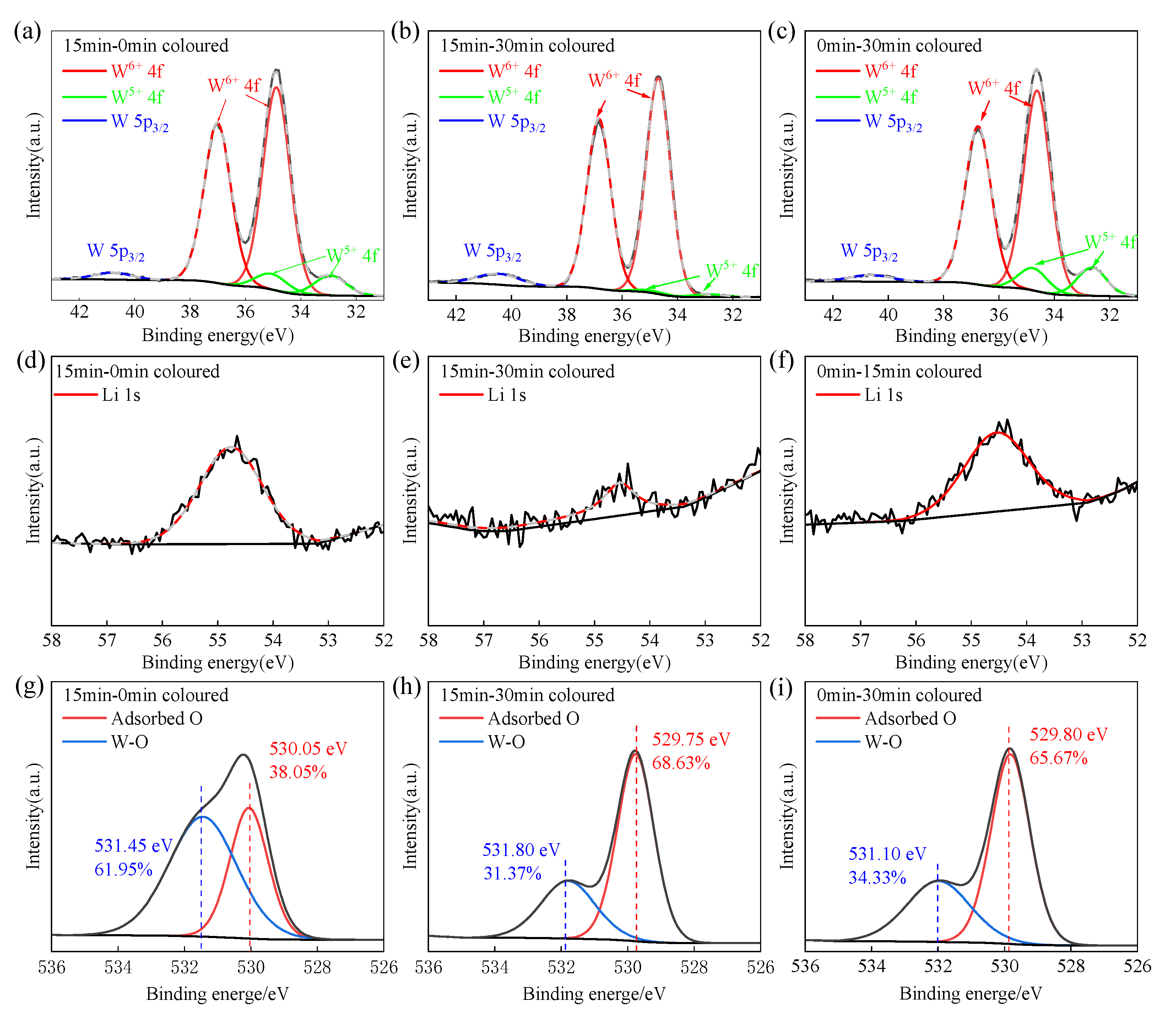
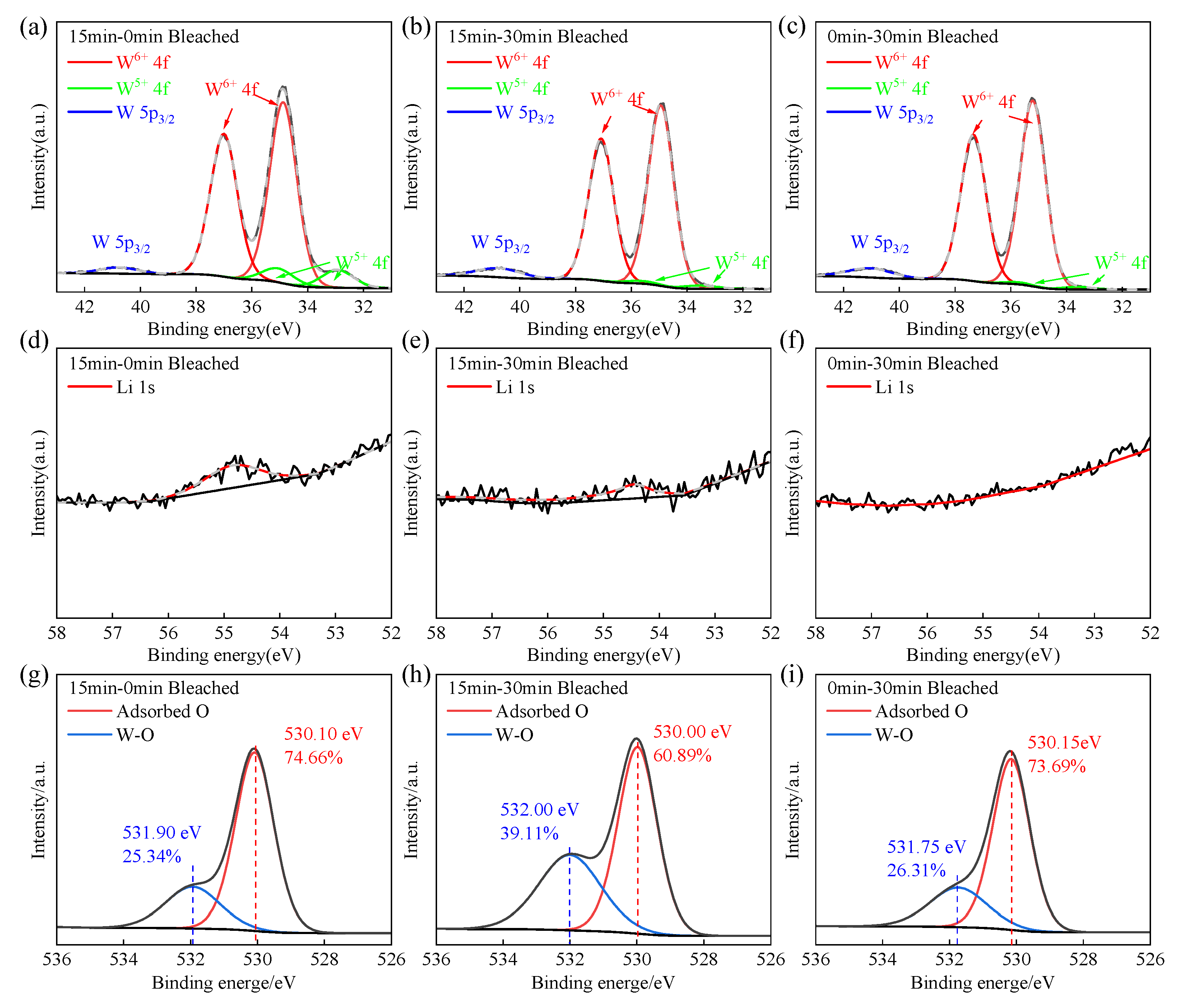
The optical modulation characteristics of the phase-engineered WO3 films were evaluated using a custom-built electrochromic device with the following configuration: ITO glass coated with WO3 thin films (cathode) was used as Working Electrode, platinum foil (anode, 99.99% purity, 0.1 mm thickness) was used as Counter Electrode, 1.0 M lithium perchlorate (LiClO4, 99.9% purity) in anhydrous propylene carbonate (PC) was used as Electrolyte.
The optical transmittance was measured in both the bleached (initial) and colored states under applied voltages of −0.8 V, −1.0 V, −1.2 V, and −1.4 V. As shown in Figure 6a–e, the optical modulation (ΔT) at 630 nm reached 33.72% (15 min–0 min), 44.80% (15 min––10 min), 62.71% (15 min–30 min), 76.57% (15 min–50 min), and 75.79% (0 min–30 min) at −1.0 V. Notably, the modulation amplitude exhibited a saturation trend beyond −1.0 V, indicating efficient Li+ intercalation at lower driving voltages. The strong correlation between ΔT and a-WO3 thickness confirms the dominant role of the amorphous phase in optical modulation, attributed to its higher density of active coloration sites and enhanced ion diffusion pathways [28].
To test the Cyclic Stability and Failure Mechanisms, post-cycling analysis after 600 CV cycles (±1 V, 0.05 V/s) was measured, as shown in Figure 7a–e. The modulation amplitudes of transmittance decreased after cycling, with values of 14.34% (15 min–0 min), 32.34% (15 min–10 min), 45.02% (15 min–30 min), 13.16% (15 min–50 min), and 8.34% (0 min–30 min). Notably, the single-crystalline sample shows the minimal degradation and pure amorphous film shows the catastrophic failure.
To examine the changes in the surface and cross-section of the films after cycling, the SEM morphology and cross-sectional images of the films after 600 cycles at ±1 V are shown in Figure 8a–j. Comparing the SEM images before and after cycling, it can be seen that the films without c-WO3 (0 min–30 min) and those with an excessively thick a-WO3 layer in the bilayer structure (15 min–50 min) exhibit poor morphology cycling stability, with the a-WO3 films almost completely disappearing after 600 cycles. In contrast, the single-layer c-WO3 and bilayer a-WO3/c-WO3 (15 min–0 min, 15 min–10 min, 15 min–30 min) show good morphology cycling stability, maintaining their basic structure intact after 600 cycles.

3.5. XPS Analysis

X-ray photoelectron spectroscopy (XPS) was performed to evaluate the surface chemistry and chemical bonding state of each film. The high-resolution XPS spectra in the color rendered state are shown in Figure 9a–i. It was observed that the W 4f spectra of the a-WO films could only be de-convoluted into a set of double peaks at 34.85 and 37.00 eV [29], which were attributed to the W 4f 7/2 and W 4f 5/2 orbitals of W6+, respectively, and the second double peaks at 35.05 and 32.90 eV could be attributed to W5+ [30,31]. Both monolayers of crystalline-free WO3 and crystalline WO3 showed a significant presence of W5+ in the colored state, with ratios of W5+/(W5++W6+) of 10.29% and 13.48%, respectively (Figure 9a,c). In contrast, the ratio of W5+/(W5++W6+) in bilayers (15 min–30 min) was lower at 1.84% (Figure 9b). The Li 1s spectra (Figure 9d–f) showed a higher degree of Li+ injection in monolayers of crystals and amorphous structures, whereas in bilayers with amorphous coverings the degree of Li+ injection was significantly lower. This difference may be attributed to the effect of Li+ on the coloring sites within the WO3 films [32], where some of the Li+ ions penetrate the lattice and form shallow traps that do not contribute to the film coloring, which is in agreement with Wen’s observations [33]. These findings suggest that the monolayer film achieves effective Li+ embedding, leading to the subsequent reduction in W6+ to W5+. The biphasic heterostructured films exhibit significant surface w-ion valence stability, suggesting the presence of an interfacial charge transfer mechanism at the amorphous/crystalline boundary. Furthermore, the high-resolution XPS spectra of O 1s can be decomposed into two peaks, where the main peak at about 530.0 eV can be attributed to the lattice oxygen of the W-O bond in WO3 [34], while the additional shoulder peak near 532.0 eV can be assigned to the surface-adsorbed O [35], especially around the oxygen vacancy region. o1s spectral analysis (Figure 9g–i) reveals that the bilayer structure exhibits the same oxygen state as the monolayer crystalline WO3 film-comparable oxygen states, while the monolayer amorphous membranes exhibit higher adsorbed oxygen content [36].
Figure 10a–i presents the XPS spectra of W 4f, Li 1s, and O 1s in the bleached state. As depicted in Figure 10a–c, upon applying a bleaching voltage of +1 V, the chemical valence of W undergoes a transformation. Notably, a certain proportion of W5+ persists in the single-layer crystalline WO3 film, enabling it to retain a colored state. In contrast, the content of W5+ is markedly lower in both the bilayer structure with an amorphous layer and the single-layer amorphous WO3 film [37]. Figure 10d–f illustrates the XPS spectra of Li 1s, providing clear insight into the residual Li+ content. The single-layer crystalline film appears to retain a substantial amount of residual Li+, and based on prior transmittance analysis, the film fails to revert to a fully transparent state. This residual Li+ may account for the film’s inability to achieve complete transparency. As observed in the O 1s spectra in Figure 10g–i, the relative content of adsorbed oxygen in the single-layer crystalline WO3 film exhibits a significant reduction compared to the colored state. Conversely, the changes in oxygen vacancies during the bleaching and coloring processes are less pronounced in both the bilayer film with an amorphous layer and the single-layer amorphous film [38]. The observed results reveal distinct ion diffusion pathways in amorphous and crystalline WO3 films [39]. The amorphous WO3 film demonstrates preferential ion insertion but exhibits limited ion extraction capability. In contrast, the crystalline film shows poor ion insertion efficiency; however, once ions are intercalated, they nearly vanish after exsolution, likely due to rapid ion release facilitated by the ordered lattice structure. This divergence highlights the critical role of material crystallinity in governing ion transport dynamics and retention behavior.

4. Conclusions

In conclusion, this study successfully addresses the longstanding trade-off between coloration efficiency and cycling durability in WO3 electrochromic films by introducing a phase-engineered amorphous/crystalline bilayer architecture [40]. Through precise phase-boundary modulation via magnetron sputtering and thermal annealing, the heterostructure WO3 film synergistically combines the high coloration efficiency of amorphous phases with the structural robustness of crystalline phases. The optimized bilayer configuration (148 nm amorphous upper layer/115 nm crystalline lower layer) achieves an exceptional light modulation range of 62.71%, along with significantly enhanced cycling stability that retains 45.02% optical modulation after 600 cycles. Multimodal characterization reveals that the improved performance originates from efficient interfacial charge transfer and phase-tailored ion diffusion pathways, which mitigate irreversible structural degradation [41]. This crystal-phase engineering strategy not only overcomes conventional material limitations but also establishes a universal framework for designing next-generation electrochromic devices with customizable optical dynamics and extended operational lifetimes [42], paving the way for practical applications in energy-efficient smart windows and adaptive optical systems.

Author Contributions

Conceptualization, X.C.; Methodology, K.L. and Z.Y.; Formal analysis, K.L. and H.Z.; Investigation, Y.C.; Data curation, C.W.; Writing—original draft, X.C.; Writing—review and editing, X.Y.; Funding acquisition, X.Y. All authors have read and agreed to the published version of the manuscript.

Funding

This work was supported by Science and Technology Development Project of Jilin Province, China (No. 20220201068GX).

Data Availability Statement

Data is contained within the article.

Conflicts of Interest

The authors declare no conflicts of interest.

References

  1. Khandelwal, H.; Schenning, A.P.H.J.; Debije, M.G. Infrared Regulating Smart Window Based on Organic Materials. Adv. Energy Mater. 2017, 7, 1602209–1602227. [Google Scholar] [CrossRef]
  2. Cannavale, A.; Ayr, U.; Fiorito, F.; Martellotta, F. Smart Electrochromic Windows to Enhance Building Energy Efficiency and Visual Comfort. Energies 2020, 13, 1449–1466. [Google Scholar] [CrossRef]
  3. Wang, Z.; Wang, X.; Cong, S.; Geng, F.; Zhao, Z. Fusing electrochromic technology with other advanced technologies: A new roadmap for future development. Mater. Sci. Eng. R Rep. 2020, 140, 100524–100550. [Google Scholar] [CrossRef]
  4. Primiceri, V.; Pugliese, M.; Giannuzzi, R.; Esposito, M.; Gigli, G.; Maiorano, V.; Cossari, P. Enhanced Durability of an All-Solid-State WO3 Based Electrochromic Device on a Single Substrate by Using a Complementary Anodically Coloring Poly(o-ethoxyaniline). ACS Appl. Electron. Mater. 2023, 5, 5735–5748. [Google Scholar] [CrossRef]
  5. Shin, D.; Kim, J.; Choi, S.; Song, G.; Rougier, A.; Lee, C.S. Evaluation of low-voltage-driven multi-colored electrochromic device based on dry-deposited V2O5. Sol. Energy Mater. Sol. Cells 2023, 257, 112341–112368. [Google Scholar] [CrossRef]
  6. Lv, Z.; Yang, D.; Mo, J.; Jin, Z.; Chang, S. Construction of TiO2/WO3/TiO2 double heterojunction films for excellent electrochromic performance. Sci. Rep. 2024, 14, 11443–11452. [Google Scholar] [CrossRef]
  7. Gao, G.; Tao, X.; He, Y.; Li, Z.; Zhuang, J.; He, L.; Li, Y.; Wang, Y.; Sun, D.; Xie, A. Electrochromic composites films composed of MoO3 doped by tungsten atoms with remarkable response speed and color rendering efficiency via electrochemical deposition. Appl. Surf. Sci. 2023, 640, 158346. [Google Scholar] [CrossRef]
  8. Dong, D.; Djaoued, H.; Vienneau, G.; Robichaud, J.; Brown, D.; Brüning, R.; Djaoued, Y. Electrochromic and colorimetric properties of anodic NiO thin films: Uncovering electrochromic mechanism of NiO. Electrochim. Acta 2020, 335, 135648–135659. [Google Scholar] [CrossRef]
  9. Zhao, Y.; Zhang, X.; Li, W.; Li, Z.; Zhang, H.; Chen, M.; Sun, W.; Xiao, Y.; Zhao, J.; Li, Y. High-performance electrochromic WO3 film driven by controllable crystalline structure and its all-solid-state device. Sol. Energy Mater. Sol. Cells 2022, 237, 111564. [Google Scholar] [CrossRef]
  10. Xie, Z.; Liu, Q.; Zhang, Q.; Lu, B.; Zhai, J.; Diao, X. Fast-switching quasi-solid state electrochromic full device based on mesoporous WO3 and NiO thin films. Sol. Energy Mater. Sol. Cells 2019, 200, 110017–110025. [Google Scholar] [CrossRef]
  11. Zhang, Z.; Mo, H.; Li, R.; Zhou, X.; Lin, Z.; Zhang, J.; Tang, X.; Zhan, Y.; Luo, J. The Counterbalancing Role of Oxygen Vacancy between the Electrochromic Properties and the Trapping Effect Passivation for Amorphous Tungsten Oxide Films. Small Sci. 2024, 4, 2300219–2300231. [Google Scholar] [CrossRef]
  12. Shi, Y.; Sun, M.; Zhang, Y.; Cui, J.; Shu, X.; Wang, Y.; Qin, Y.; Liu, J.; Tan, H.H.; Wu, Y. Rational Design of Oxygen Deficiency-Controlled Tungsten Oxide Electrochromic Films with an Exceptional Memory Effect. ACS Appl. Mater. Interfaces 2020, 12, 32658–32665. [Google Scholar] [CrossRef] [PubMed]
  13. Zhang, R.; Zhou, Q.; Huang, S.; Zhang, Y.; Wen, R.-T. Capturing ion trapping and detrapping dynamics in electrochromic thin films. Nat. Commun. 2024, 15, 2294–2306. [Google Scholar] [CrossRef] [PubMed]
  14. Tang, C.; Liu, H.; Cai, C. Exploring the electronic structure and lithium diffusion kinetics of amorphous tungsten oxide. AIP Adv. 2024, 14, 095117–095122. [Google Scholar] [CrossRef]
  15. Zhou, D.; Xie, D.; Shi, F.; Wang, D.; Ge, X.; Xia, X.; Wang, X.; Gu, C.; Tu, J. Crystalline/amorphous tungsten oxide core/shell hierarchical structures and their synergistic effect for optical modulation. J. Colloid Interface Sci. 2015, 460, 200–208. [Google Scholar] [CrossRef]
  16. Huo, X.; Zhang, H.; Shen, W.; Miao, X.; Zhang, M.; Guo, M. Bifunctional aligned hexagonal/amorphous tungsten oxide core/shell nanorod arrays with enhanced electrochromic and pseudocapacitive performance. J. Mater. Chem. A 2019, 7, 16867–16875. [Google Scholar] [CrossRef]
  17. Poongodi, S.; Kumar, P.S.; Mangalaraj, D.; Ponpandian, N.; Meena, P.; Masuda, Y.; Lee, C. Electrodeposition of WO3 nanostructured thin films for electrochromic and H2S gas sensor applications. J. Alloys Compd. 2017, 719, 71–81. [Google Scholar] [CrossRef]
  18. Kumar, K.N.; Sattar, S.A.; Shaik, H.; Reddy, G.V.A.; Jafri, R.I.; Merum, D.; Pawar, A.S.; Nunna, G.P.; Premkumar, R.; Ansar, S.; et al. Effect of partial pressure of oxygen, target current, and annealing on DC sputtered tungsten oxide (WO3) thin films for electrochromic applications. Solid State Ion. 2023, 399, 116275. [Google Scholar] [CrossRef]
  19. Liu, Z.; Yamazaki, T.; Shen, Y.; Kikuta, T.; Nakatani, N. Influence of annealing on microstructure and NO2-sensing properties of sputtered WO3 thin films. Sens. Actuators B Chem. 2007, 128, 173–178. [Google Scholar] [CrossRef]
  20. Efkere, H.İ.; Gümrükçü, A.E.; Özen, Y.; Kınacı, B.; Aydın, S.Ş.; Ates, H.; Özçelik, S. Investigation of the effect of annealing on the structural, morphological and optical properties of RF sputtered WO3 nanostructure. Phys. B Condens. Matter 2021, 622, 413350–413358. [Google Scholar] [CrossRef]
  21. Chen, X.; Li, W.; Wang, L.; Zhao, Y.; Zhang, X.; Li, Y.; Zhao, J. Annealing effect on the electrochromic properties of amorphous WO3 films in Mg2+ based electrolytes. Mater. Chem. Phys. 2021, 270, 124745–124752. [Google Scholar] [CrossRef]
  22. Xu, J.; Li, X.; Zhang, Y.; Zhang, X.; Liu, J.; Wu, Y. Effect of In Situ Heating on the Growth and Electrochromic Properties of Tungsten Trioxide Thin Films. Materials 2024, 17, 2214. [Google Scholar] [CrossRef] [PubMed]
  23. Salim, E.T.; Hassan, A.I.; Mohamed, F.A.; Wahid, M.H.A.; Fakhri, M.A. A sight of view on electrical impacts, structural properties and surface roughness of tungsten trioxide thin film: Effect of substrate temperatures in WO3/Si device fabrication. Phys. Scr. 2023, 98, 035508. [Google Scholar] [CrossRef]
  24. Xu, X.; Zhang, J.; Zhang, Z.; Lu, G.; Cao, W.; Wang, N.; Xia, Y.; Feng, Q.; Qiao, S. All-Covalent Organic Framework Nanofilms Assembled Lithium-Ion Capacitor to Solve the Imbalanced Charge Storage Kinetics. Nano-Micro Lett. 2024, 16, 116–131. [Google Scholar] [CrossRef]
  25. Zhang, S.; Peng, Y.; Zhao, J.; Fan, Z.; Ding, B.; Lee, J.Y.; Zhang, X.; Xuan, Y. Amorphous and Porous Tungsten Oxide Films for Fast-Switching Dual-Band Electrochromic Smart Windows. Adv. Opt. Mater. 2022, 11, 2202115. [Google Scholar] [CrossRef]
  26. Guo, T.; Hu, P.; Li, L.; Wang, Z.; Guo, L. Amorphous materials emerging as prospective electrodes for electrochemical energy storage and conversion. Chem 2023, 9, 1080–1093. [Google Scholar] [CrossRef]
  27. Atak, G.; Pehlivan, I.B.; Montero, J.; Granqvist, C.G.; Niklasson, G.A. Electrochromic tungsten oxide films prepared by sputtering: Optimizing cycling durability by judicious choice of deposition parameters. Electrochim. Acta 2021, 367, 137233–137267. [Google Scholar] [CrossRef]
  28. Sychov, M.; Eruzin, A.; Semenova, A.; Katashev, P.; Mjakin, S.; Zhukov, M.V.; Aglikov, A.; Nosonovsky, M.; Skorb, E.V. Deposition of Nanostructured Tungsten Oxide Layers by a New Method: Periodic Modulation of the Deposition Angle. Langmuir 2023, 39, 12336–12345. [Google Scholar] [CrossRef]
  29. Wang, K.; Luo, L.; Wang, C.; Tang, J. Photocatalytic methane activation by dual reaction sites co-modified WO3. Chin. J. Catal. 2023, 46, 103–112. [Google Scholar] [CrossRef]
  30. Hu, X.; Li, X.; Yang, H.; Liu, S.; Qin, Z.; Xie, C.; Zeng, D. Active edge effect of pothole-rich WO3 nanosheets for enhancing dimethyl trisulfide gas sensing performance. Sens. Actuators B Chem. 2022, 352, 131103–131112. [Google Scholar] [CrossRef]
  31. Wang, Q.; Li, R.; Wang, P.; Zhang, Y.; Wang, Y.; Yang, Y.; Wu, Z.; An, B.; Li, J.; Xie, E. Au-decorated WO3-based sensor for chemiresistive detection of NO2 at 80 °C. Sens. Actuators B Chem. 2023, 390, 133985–133998. [Google Scholar] [CrossRef]
  32. Heo, S.; Dahlman, C.J.; Staller, C.M.; Jiang, T.; Dolocan, A.; Korgel, B.A.; Milliron, D.J. Enhanced Coloration Efficiency of Electrochromic Tungsten Oxide Nanorods by Site Selective Occupation of Sodium Ions. Nano Lett. 2020, 20, 2072–2079. [Google Scholar] [CrossRef] [PubMed]
  33. Wen, R.-T.; Niklasson, G.A.; Granqvist, C.G. Sustainable Rejuvenation of Electrochromic WO3 Films. ACS Appl. Mater. Interfaces 2015, 7, 28100–28104. [Google Scholar] [CrossRef]
  34. Subramani, T.; Thimmarayan, G.; Balraj, B.; Chandrasekar, N.; Palanisamy, M.; Nagarajan, S.K.; Amirtharajan, S.; Kumar, M.; Sivakumar, C. Surfactants assisted synthesis of WO3 nanoparticles with improved photocatalytic and antibacterial activity: A strong impact of morphology. Inorg. Chem. Commun. 2022, 142, 109709. [Google Scholar] [CrossRef]
  35. Jin, Y.; Chen, Z.; Yang, L.; Zhang, K.; Ma, T.; Zhang, S.; Dai, W.; Luo, S. Implanted-Electron-hydrogen boosted breaking of W–O bonds to generate crater/oxygen vacancy filled WO3 nanoflakes for efficient oxidation of emerging pollutant. J. Alloys Compd. 2022, 890, 161831. [Google Scholar] [CrossRef]
  36. Su, J.; Zhu, X.; Chen, L.; Liu, Y.; Qi, H.; He, Z.; Tang, B. Optimization of Optical Modulation in Amorphous WO3 Thin Films. Electron. Mater. Lett. 2024, 20, 131–139. [Google Scholar] [CrossRef]
  37. Shi, Y.; Sun, M.; Zhang, Y.; Cui, J.; Wang, Y.; Shu, X.; Qin, Y.; Tan, H.H.; Liu, J.; Wu, Y. Structure modulated amorphous/crystalline WO3 nanoporous arrays with superior electrochromic energy storage performance. Sol. Energy Mater. Sol. Cells 2020, 212, 110579–110589. [Google Scholar] [CrossRef]
  38. Guillén, C.; Herrero, J. Amorphous WO3-thin films with color characteristics tuned by the oxygen vacancies created during reactive DC sputtering. J. Mater. Sci. Technol. 2021, 78, 223–228. [Google Scholar] [CrossRef]
  39. Zhang, M.; Yang, C.; Zhang, Z.; Tian, W.; Hui, B.; Zhang, J.; Zhang, K. Tungsten oxide polymorphs and their multifunctional applications. Adv. Colloid Interface Sci. 2022, 300, 102596. [Google Scholar] [CrossRef]
  40. Zhang, Y.; Liang, X.; Jiang, T.; Liu, H.; Fu, Y.; Zhang, D.; Geng, Z. Amorphous/crystalline WO3 dual phase laminated films: Fabrication, characterization and evaluation of their electrochromic performance for smart window applications. Sol. Energy Mater. Sol. Cells 2022, 244, 111820. [Google Scholar] [CrossRef]
  41. Wang, Z.; Chen, G.; Zhang, H.; Liang, L.; Gao, J.; Cao, H. In situ TEM investigation of hexagonal WO3 irreversible transformation to Li2WO4. Scr. Mater. 2021, 203, 114090–114095. [Google Scholar] [CrossRef]
  42. Gu, C.; Jia, A.-B.; Zhang, Y.-M.; Zhang, S.X.-A. Emerging Electrochromic Materials and Devices for Future Displays. Chem. Rev. 2022, 122, 14679–14721. [Google Scholar] [CrossRef]
Figure 1. Flow chart illustrating the preparation process of phase-engineered bilayer WO3 thin films.
Crystals 15 00324 g001
Figure 2. XRD spectra of WO3 thin films in amorphous and crystalline states with varying thicknesses.
Crystals 15 00324 g002
Figure 3. Surface SEM images of WO3 films with different amorphous/crystal thickness ratios (a) 15 min–0 min, (b) 15 min–10 min, (c) 15 min–30 min, (d) 15 min–50 min, (e) 0 min–30 min; cross–section SEM images (f) 15 min–0 min, (g) 15 min–10 min, (h) 15 min–30 min, (i) 15 min–50 min, (j) 0 min–30 min.
Crystals 15 00324 g003
Figure 4. Cyclic voltammetry (CV) curves of WO3 films at different scan rates: (a) 15 min–0 min, (b) 15 min–10 min, (c) 15 min–30 min, (d) 15 min–50 min, and (e) 0 min–30 min and (f) the relationship between the peak cathodic current and the square root of the scan rate.
Crystals 15 00324 g004
Figure 5. Cyclic voltammetry (CV) curves of WO3 films scanned at 0.05 V/s after 600 cycles: (a) 15 min–0 min, (b) 15 min–10 min, (c) 15 min–30 min, (d) 15 min–50 min, and (e) 0 min–30 min.
Crystals 15 00324 g005
Figure 6. Transmittance spectra of WO3 films under different coloring voltages and at −1 V after coloring, with corresponding photographs: (a) 15 min–0 min, (b) 15 min–10 min, (c) 15 min–30 min, (d) 15 min–50 min, and (e) 0 min–30 min.
Crystals 15 00324 g006
Figure 7. Transmittance spectra of WO3 films after 600 electrochemical cycles: (a) 15 min–0 min, (b) 15 min–10 min, (c) 15 min–30 min, (d) 15 min–50 min, and (e) 0 min–30 min.
Crystals 15 00324 g007
Figure 8. SEM images of WO3 film surface after 600 electrochemical cycles: (a) 15 min–0 min, (b) 15 min–10 min, (c) 15 min–30 min, (d) 15 min–50 min, (e) 0 min–30 min; SEM images of cross–section (f) 15 min–0 min, (g) 15 min–10 min, (h) 15 min–30 min, (i) 15 min–50 min, (j) 0 min–30 min.
Crystals 15 00324 g008
Figure 9. XPS spectra of (ac) W 4f, (df) Li 1s, and (gi) O 1s in the colored states of 15 min–0 min, 15 min–30 min, and 0 min–30 min.
Crystals 15 00324 g009
Figure 10. XPS spectra of (ac) W 4f, (df) Li 1s, and (gi) O 1s in the discoloration states of 15 min–0 min, 15 min–30 min, and 0 min–30 min.
Crystals 15 00324 g010
Disclaimer/Publisher’s Note: The statements, opinions and data contained in all publications are solely those of the individual author(s) and contributor(s) and not of MDPI and/or the editor(s). MDPI and/or the editor(s) disclaim responsibility for any injury to people or property resulting from any ideas, methods, instructions or products referred to in the content.

