Abstract
Based on the friction phenomenon, this study proposes a new method for localized electrodeposition preparation and prepares Cu-SiC composite deposited layers on copper substrates. The morphology of the deposited layer was observed using optical microscopy; the physical phase of the deposited layer was analyzed by X-ray diffraction; and the microstructure and size of the deposited layer were examined using scanning electron microscopy. The wear resistance of the deposited layer was evaluated through friction and wear experiments. The study found that the friction speed significantly influenced the morphology and size of the deposited layer. At a friction speed of 40 mm/s, the width of the deposited layer increased by 68.7%. Under the friction effect, the wear resistance of the deposited layer was improved. The coefficient of friction and wear width were reduced by 25.6% and 21.2%, respectively. The electrodeposited layer microstructure indicates that increasing the friction speed helps refine the microstructure. This has a significant impact on improving the performance of the electrodeposited layer.
1. Introduction
Electrochemical additive deposition is an advanced surface deposition preparation technology that combines the concepts of electrochemical deposition and additive manufacturing [1,2]. It deposits metal or composite materials precisely in a specified area by layer-by-layer deposition. In the fields of machinery, aerospace, etc., selective electrodeposition technology can be used to improve the corrosion resistance and service life of equipment. In the field of electronic packaging, electrochemical additive deposition technology can be used to prepare packaging materials with excellent conductivity and corrosion resistance [3]. Composite electrodeposition technology is an important component of electrodeposition. It has attracted much attention due to its high hardness, wear resistance, corrosion resistance, special decorative appearance, electrical contact, electrocatalysis, and other functions. The commonly used matrix metals for composite electroplating are nickel, copper, chromium, iron, etc., and the main dispersed phases are metal oxides, carbides, nitrides, and polymer particles [4]. The most widely studied is the composite deposition with copper as the matrix and inorganic compound particles as the reinforcement phase. Among them, the Cu-SiC composite electrodeposition layer has been successfully applied to the automotive and aerospace industries due to its excellent corrosion resistance and tribological properties [5]. The application of localized electrodeposition technology in the preparation of the composite deposited layer can have broad prospects.
Electrodeposition can be carried out continuously at room temperature, and the deposited layer formed has low internal stress, good processing surface quality, no thermal deformation, no crack defects, etc. The characteristic that electrodeposition can be formed at room temperature gives it a great advantage over technologies such as laser manufacturing. It can avoid the conventional additive manufacturing technology that uses laser and electron beam as a heat source to cause high thermal residual stress, oxidation phase transformation segregation, pores, cracks, inclusions, confusion, poor mechanical properties, and low dimensional accuracy of the formed parts [6]. It can also take advantage of the fact that the material transfer in the electrochemical deposition process is carried out at the ion scale, which can achieve the advantages of micro–nano processing accuracy, thereby realizing the processing goals of high-precision and complex three-dimensional (3D) metal microstructures [7]. Traditional electrochemical additive deposition methods mainly include jet electrochemical deposition and fluid force microscope (FM) technology [8,9]. For example, Van Nisselroy et al. [10] used fluid force microscope (FM) technology to prepare a three-dimensional nickel microstructure by one-step electrochemical deposition. Maskless localized electrochemical deposition is an important research direction in the field of localized electrodeposition [11]. This technology does not require masks and support structures in the process of depositing layers. It is carried out in a “direct writing” manner, or a small diameter nozzle is used as the anode, and the movement trajectory of the fine electrolyte beam relative to the cathode is controlled by a computer to complete the electrochemical deposition–additive manufacturing process. There are no complicated processes such as the production, stacking, and removal of masks (plates) and support structures. Therefore, it has the advantages of a simple process and can be deposited at any position on the conductive substrate [12]. Due to the great process difficulty, challenging research content, and broad application prospects of maskless localized electrochemical deposition–additive manufacturing technology, it has become a hot spot in the field of localized electrochemical deposition technology. In addition, the technology of combining laser induction with electrodeposition can also be deposited locally on the cathode [13,14,15]. However, the substrate can be damaged under the effect of the laser; the equipment required is expensive; and further research in this area needs to be explored. In summary, the current localized electrodeposition technology is mainly used in the manufacture of micro–nano structures. There is still little research on the use of localized deposition-related technologies to form functional protective layers on the surface of materials. In addition, the current localized electrochemical deposition technology has the characteristics of slow manufacturing speed and low deposition efficiency, and research on functional protective layers on deposition surfaces needs further exploration.
To further explore the problem of preparing a functional deposited layer using localized electrodeposition methods, this study proposed a new localized electrodeposition method. Through the friction between electrodes, the Cu-SiC composite deposited layer was deposited on the copper substrate, improving the performance of the substrate. This study combines friction and electrodeposition and proposes an electrodeposition method based on the friction effect. This method uses the friction effect to deposit a composite layer on a metal substrate. Compared with the existing localized electrodeposition technology, it has the characteristics of simple equipment and high deposition efficiency.
2. Materials and Experiments
2.1. Materials and Electrodeposition Process
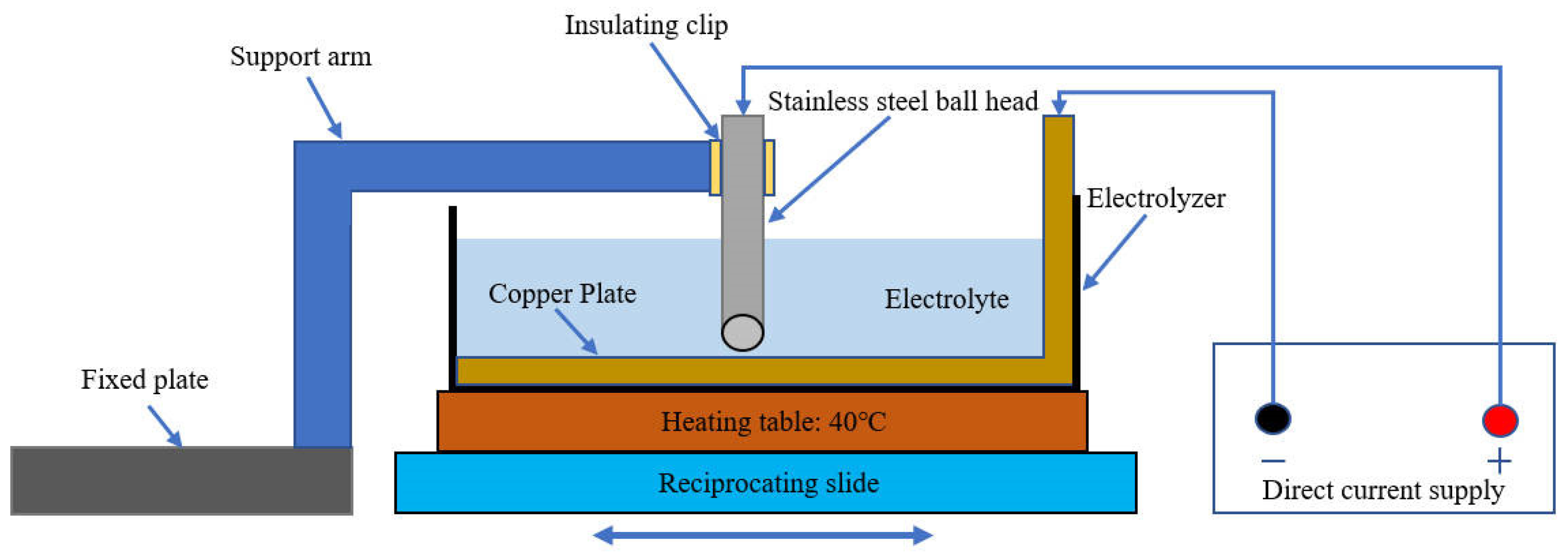
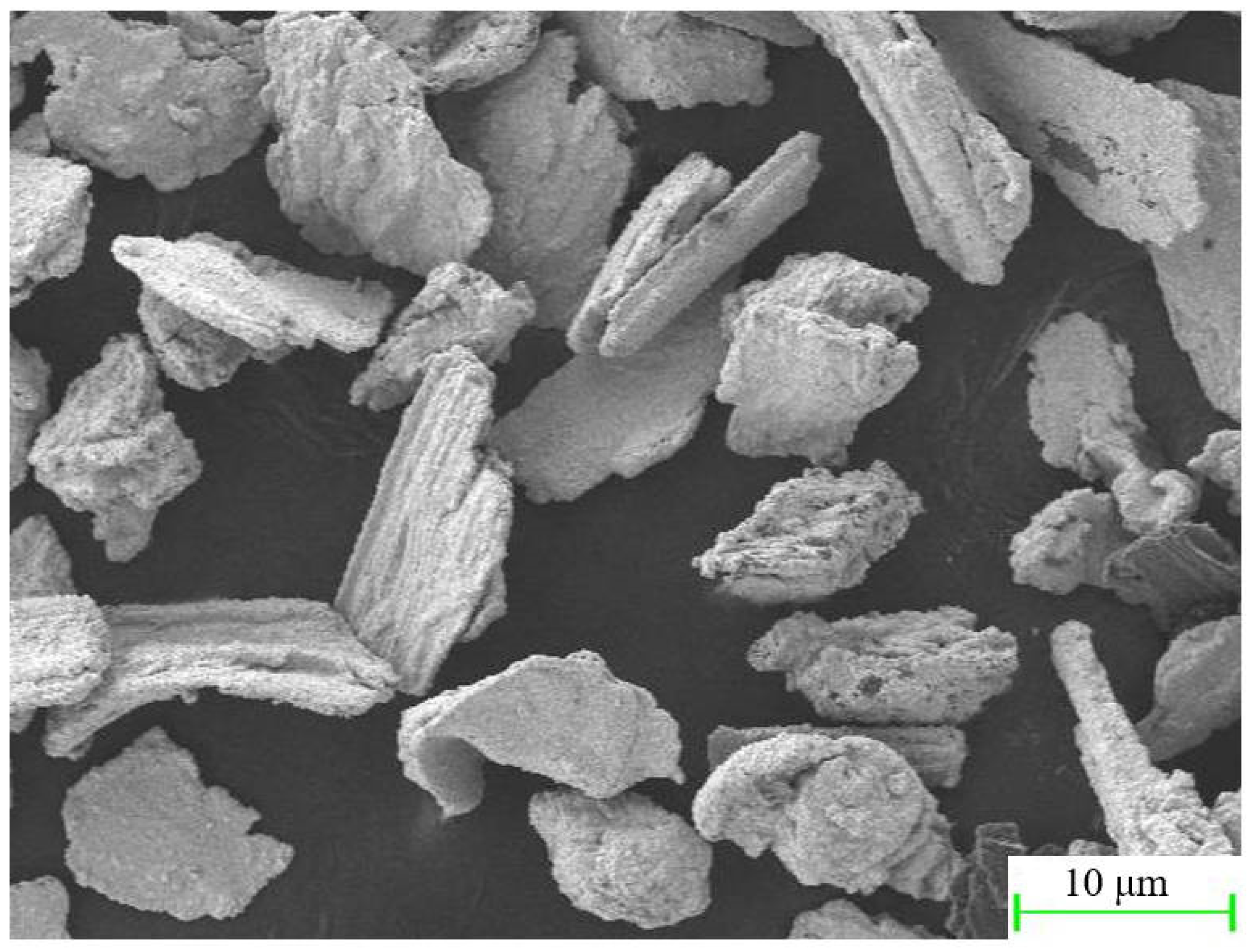
The friction-assisted electrodeposition process is shown in Figure 1. The cathode is a copper plate with a thickness of 1.5 mm, which is connected to the negative electrode of the direct current (DC) power supply. The anode is a stainless steel ball head rod, and the top is connected to the positive electrode of the DC power supply. The chemical composition of the stainless steel ball head rod is shown in Table 1. The ball head size is 20 mm in diameter, and the distance from the copper plate is set to 2 mm. The bottom of the electrolytic cell is a heater, which heats the electrolytic cell during the electrodeposition process, and the temperature is set to 40 °C. The electrolytic cell and the heater are closely connected and are driven by a reciprocating sliding mechanism during the electrolysis process, and reciprocating motion with a stroke of 60 mm. In addition, the ball head stainless steel rod is clamped by a fixed support mechanism and fixed in the middle of the electrolytic cell. The DC is set to 80 mA/cm2. To reveal the effect of friction speed on the electrodeposited layer, samples S1–S4 were set up, and their friction speeds were 10 mm/s, 20 mm/s, 30 mm/s, and 40 mm/s, respectively. The chemical composition and content of the electrolyte are shown in Table 2. The size of SiC is a mixture of 3 μm, 5 μm, and 10 μm, and the morphology of SiC is shown in Figure 2.

Figure 1.
The friction-assisted electrodeposition process.

Table 1.
The chemical composition of stainless steel ball head rod (wt.%).
Table 2.
Chemical composition of electrodeposition solution.

Figure 2.
The morphology of SiC powder.
It should be noted that copper substrates are molded through a stretching process. Before the experiment, the L-shaped copper plate was fixed in the electrolytic cell and tightly integrated with it (see Figure 1). The electrolytic cell size is 11.5 × 11.5 × 10 cm. The substrate material was placed in a solution composed of 15 g/L NaOH and 25 g/L Na2CO3 for 15 min to remove surface oil stains, cleaned and blown dry, and then placed in a solution consisting of 160 g/L sulfuric acid and 80 g/L hydrogen peroxide for 30 s activation, washed with water, and dried for later use. The pH value of the solution is 3.5. Electrodeposition experiments were performed using the equipment of Figure 1. The electrodeposition time was 10 min. After electrodeposition, turn off the DC power supply, take out the plated parts, clean the surface with deionized water, and then dry them. After complete drying, store them in a vacuum.
2.2. Characterization
The morphology of the deposited layer was observed by electron microscope, and its size was measured. The phase composition of the sample was tested by X-ray diffraction (XRD, Rigaku-SmartLab, Tokyo, Japan), and the XRD is a Cu target test with a scanning range of 5 to 90 degrees and a scanning speed of 10°/min. The microstructure of the deposited layer was observed by scanning electron microscopy (SEM, ZEISS, Oberkochen, Germany); the chemical composition of the deposited layer was tested by SEM and EDS (Energy Dispersive X-ray Spectroscopy). The microhardness was measured by vickers hardness analyzer (HV-1000STA, Laizhou weiyi ExperimentalMachine Manufacturing Co., Ltd., Laizhou, China) with 200 gf loading, and 10 s holding time. The friction and wear performance of the deposited layer was tested using a reciprocating friction and wear tester (Bruker, Billerica, MA, USA). The grinding pair was Si3N4 balls, the test force was set to 10 N, the reciprocating stroke was 2 mm, the frequency was 2 Hz, and the test time was 30 min. After the friction and wear experiment, the wear morphology was observed by SEM, and the width of the wear area was observed by optical microscope (SZMN7045TR, Sunny Optical Technology (Group) Company Limited, Yuyao, China). The surface defect morphology of the anode after electrodeposition was observed using an optical microscope. The pH value of the electrolyte was tested using a pH meter (PH-100B, Lichen, Shanghai, China).
3. Results and Discussion
3.1. Phase and Morphology Characteristics
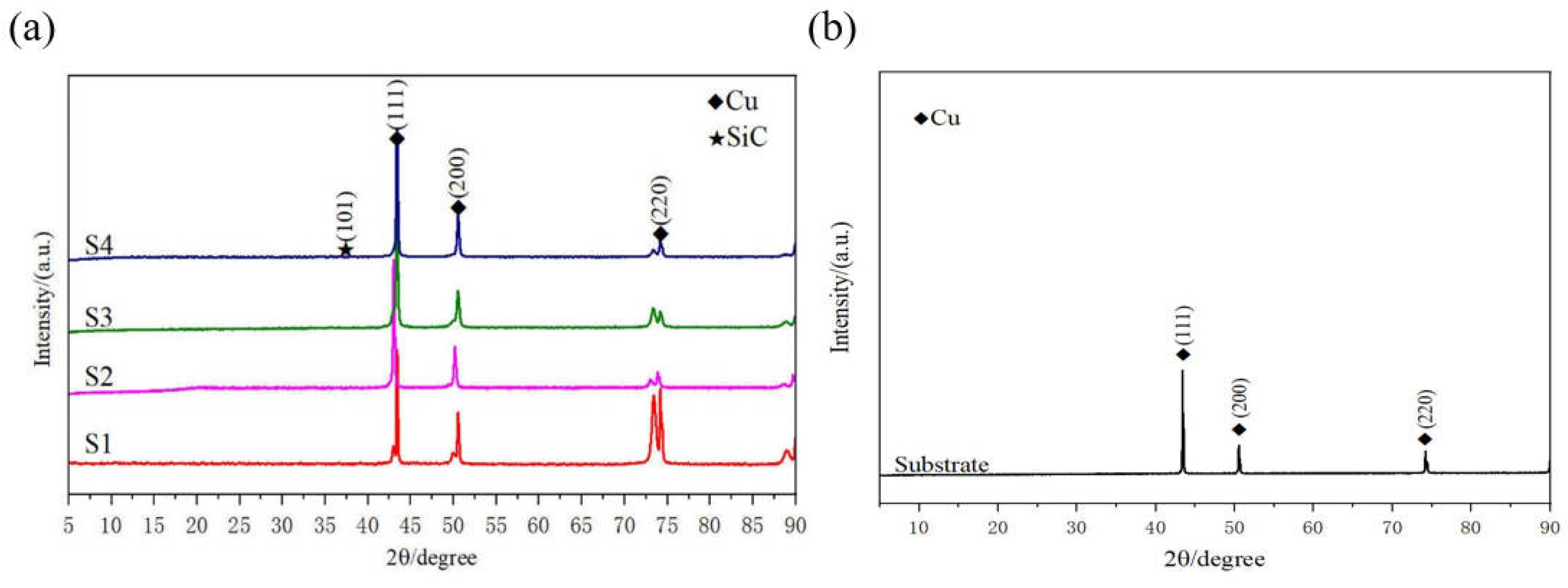
Figure 3 reveals the XRD results of the friction-assisted electrodeposition of Cu-SiC composite deposition and Cu substrate. Cu and SiC phases appear in all samples. The friction speed does not change the phase composition of the deposition layer samples. The formation of Cu is mainly because the Cu2+ in the electrolyte obtains electrons on the cathode plate under the action of the electric field and is reduced to atoms and finally deposited [16]. The flow of the electrodeposition liquid under friction stirring conditions causes the SiC solid particles to suspend and move to the vicinity of the cathode. After the particles are charged, they are electrophoresed to the cathode surface under the action of the electric field force and finally deposited on the substrate. However, during the friction electrodeposition process, the distance between the cathode and the anode is very small, and the electrolyte filled between the electrodes is turbulent, making the formation of the deposited layer in a nonlinear state. The formation of the friction-assisted electrodeposition layer mainly involves three steps (see Figure 4). Firstly, the SiC in the electrolyte is positively charged under the action of the electric field, and the SiC particles move toward the cathode surface during electrodeposition. Secondly, the positively charged SiC particles are captured by the cathode and adhere to the substrate surface. Thirdly, the SiC particles adhering to the cathode surface are squeezed with the friction ball and embedded into the substrate surface to form the deposited layer.
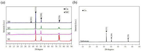
Figure 3.
XRD patterns of electrodeposited layer and substrate: (a) XRD of electrodeposited layer; (b) XRD of substrate.
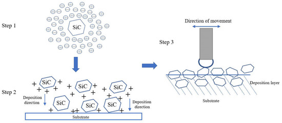
Figure 4.
The forming process of the friction-assisted electrodeposition layer.
Figure 5a reveals the morphological characteristics of the friction-assisted electrodeposition. There is an obvious deposition layer in the friction direction. It is noteworthy that the deposited layer only appears in the friction area. The length and width of the deposition layer are shown in Figure 5b. The friction speed has an important influence on the deposition size of the electrodeposited layer. As the deposition speed increases, the width and length of the deposited layer increase. The average lengths of the S1–S4 deposition layers are 7.16, 7.23, 7.26, and 7.31 mm, respectively. The average widths of the S1–S4 deposition layers are 1.57, 2.21, 2.61, and 2.65 mm, respectively. With the increase of friction speed, the width and length of the deposition layer increase. The width of the S4 sample increased by 68.7% compared to the S1 sample, while the length increased by 2.1%.
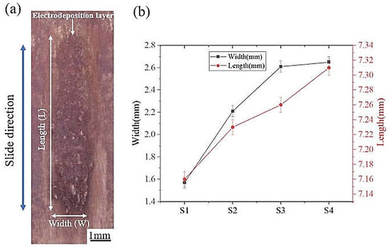
Figure 5.
(a) Morphology of electrodeposited layer; (b) Electrodeposited layer size.
3.2. Microstructure Properties
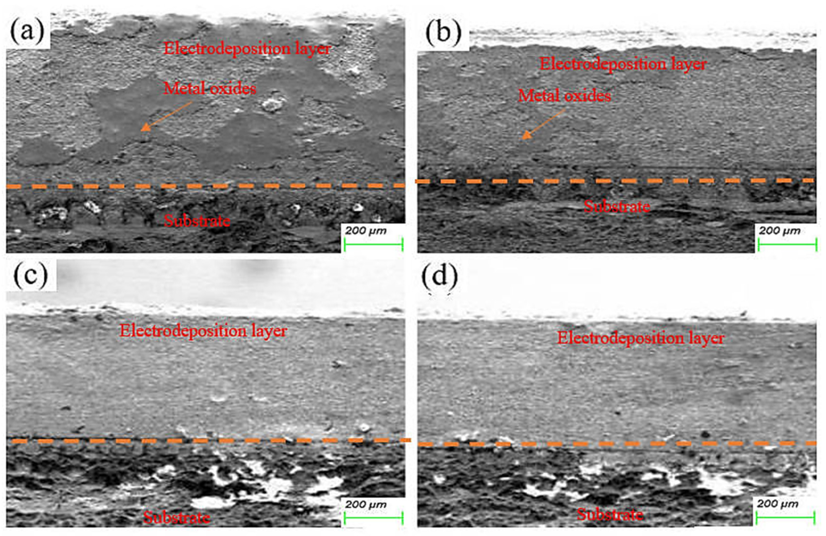
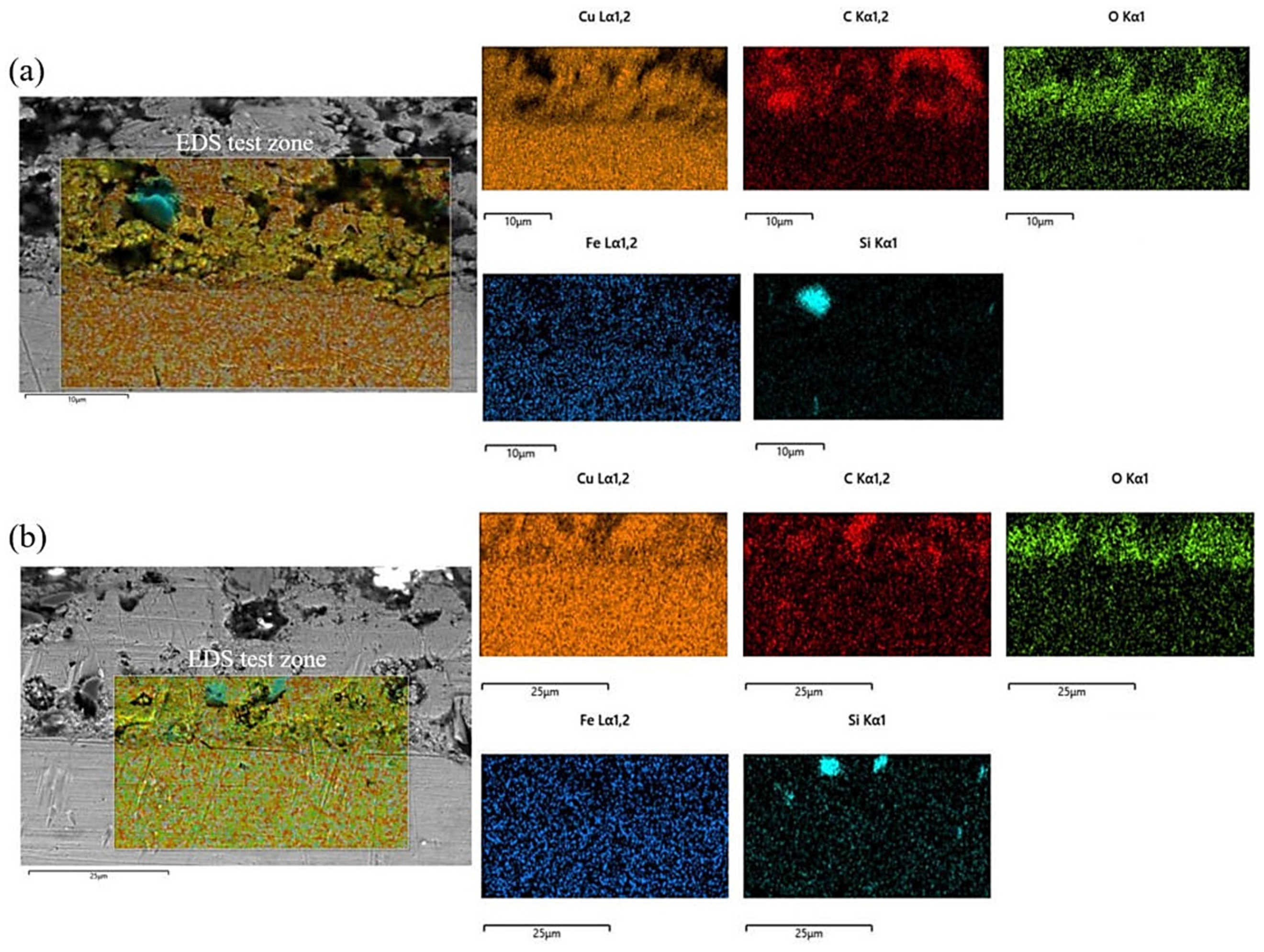
The morphology of the electrodeposited composite layer is shown in Figure 6a–d. In all samples, there is a clear boundary between the deposition and the substrate. No obvious cracks or other defects are found at the interface, which indicates that the deposition is well-deposited. To further analyze the effect of friction speed on the interface of electrodeposition, EDS was used to analyze the element distribution at the interface of deposited layer S1 and S4 samples, as shown in Figure 7. There is a more obvious void structure at the S1 interface. As the friction speed increases, the void phenomenon at the interface is alleviated. The occurrence of voids in Figure 7 is inextricably linked to the distribution of oxygen. The interfacial EDS analysis results at S1 and S4 show that oxygen is mainly enriched in the electrodeposited layer, and the distribution is not obvious in the Cu substrate. This indicates that the oxygen elements in the electrolyte diffuse differently to the deposition and the substrate during the deposition process, which produces the Kirkendall effect, resulting in the formation of voids [17]. With the increase of friction velocity, the Kirkendall effect was weakened, thus suppressing the generation of voids.

Figure 6.
Cross-sectional microstructure of electrodeposited layers: (a) S1 electrodeposited layer; (b) S2 electrodeposited layer; (c) S3 electrodeposited layer; (d) S4 electrodeposited layer.

Figure 7.
EDS analysis of the interface of electrodeposited layers: (a) S1 deposition layer; (b) S4 deposition layer.
At the S1 interface, the distribution of SiC is not obvious. As the friction speed increases, an obvious SiC distribution is detected at the interface of the deposited layer. This shows that as the friction speed increases, SiC is more easily deposited at the interface. The reason for this phenomenon may be that the increase in friction speed accelerates the aggregation of SiC on the Cu substrate, resulting in more SiC deposition at the interface. In addition, the deposition of SiC is also related to the void phenomenon at the interface of the deposited layer. The presence of voids affects the bonding between particles, making it difficult for SiC to be deposited on the substrate. The increase in friction speed alleviates this phenomenon.
The current density at the cathode under forced convection can be expressed as [18]:
where is Levich current (A), n is the number of electrons transferred, F is Faraday’s Constant, A is the surface area of the working electrode, D is diffusion coefficient of the analyte, is the angular rotation rate of the electrode, is the kinematic viscosity, C is the concentration of the analyte.
From Formula (1), it can be seen that the cathode current density can be increased by increasing the stirring speed, which has an important influence on the formation of the electrodeposition layer. Related studies have shown that the higher the cathodic limit current density, the higher the deposition rate of the electrodeposited layer [19,20]. This means that the deposition rate of the electrodeposited layer is higher as the friction velocity increases. In this study, Figure 7 shows the deposition condition at the interface between the electrodeposited layer and the substrate with different friction rates. The increase in the electrodeposition rate caused more SiC to be deposited on the substrate. At the same time, the increase in deposition rate makes it easier for metal ions in the solution to deposit and mold, reducing the voids at the interface. This has an important influence on the mechanical properties of the deposited layer.
In addition, the pH values of S1–S4 electrolytes become 9.3, 11.6, 12.1, and 13.8, respectively, during the deposition process. This means that with the increase of friction speed, the pH value of the electrode liquid increases. The H+ in the plating solution decreases under the action of friction, increasing the pH value. The higher the pH value, the stronger the conductivity of the electrolyte, which can improve the efficiency of the electrolysis process. This also reveals that with the increase of friction speed, the macroscopic size of the deposited layer also increases.
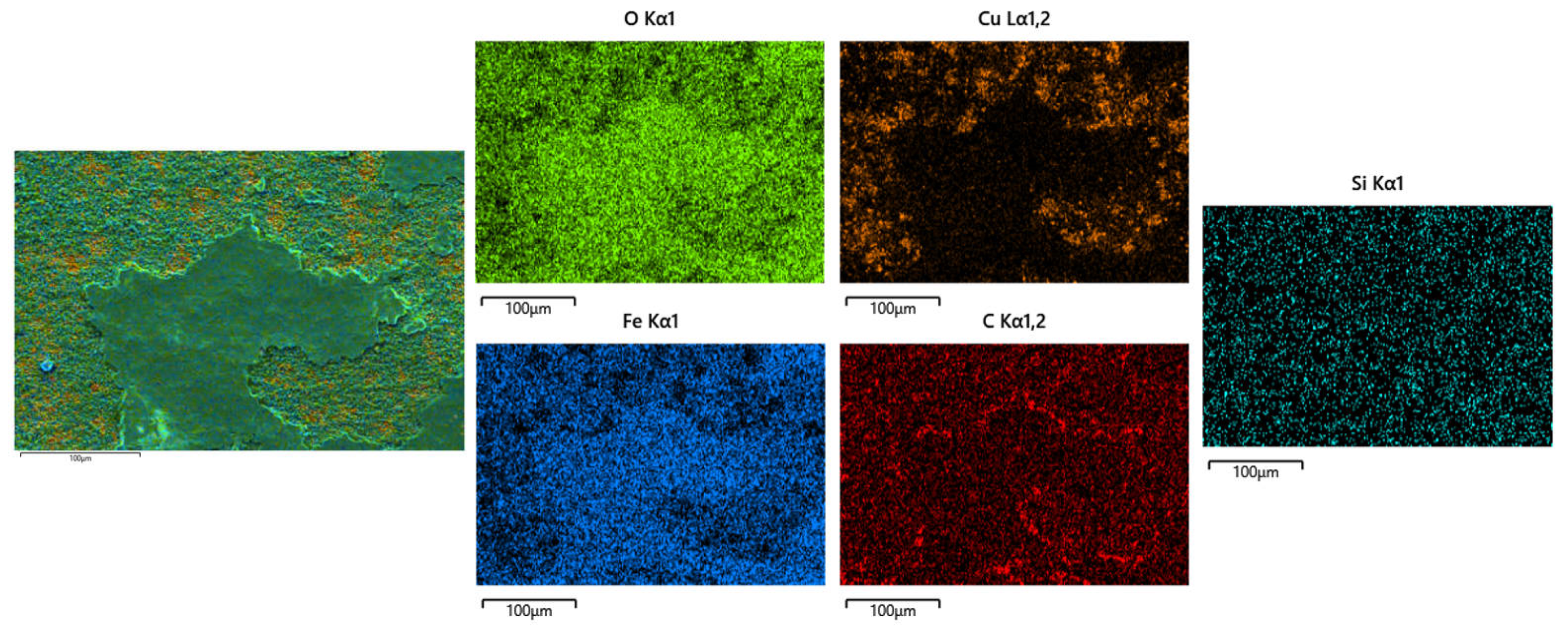
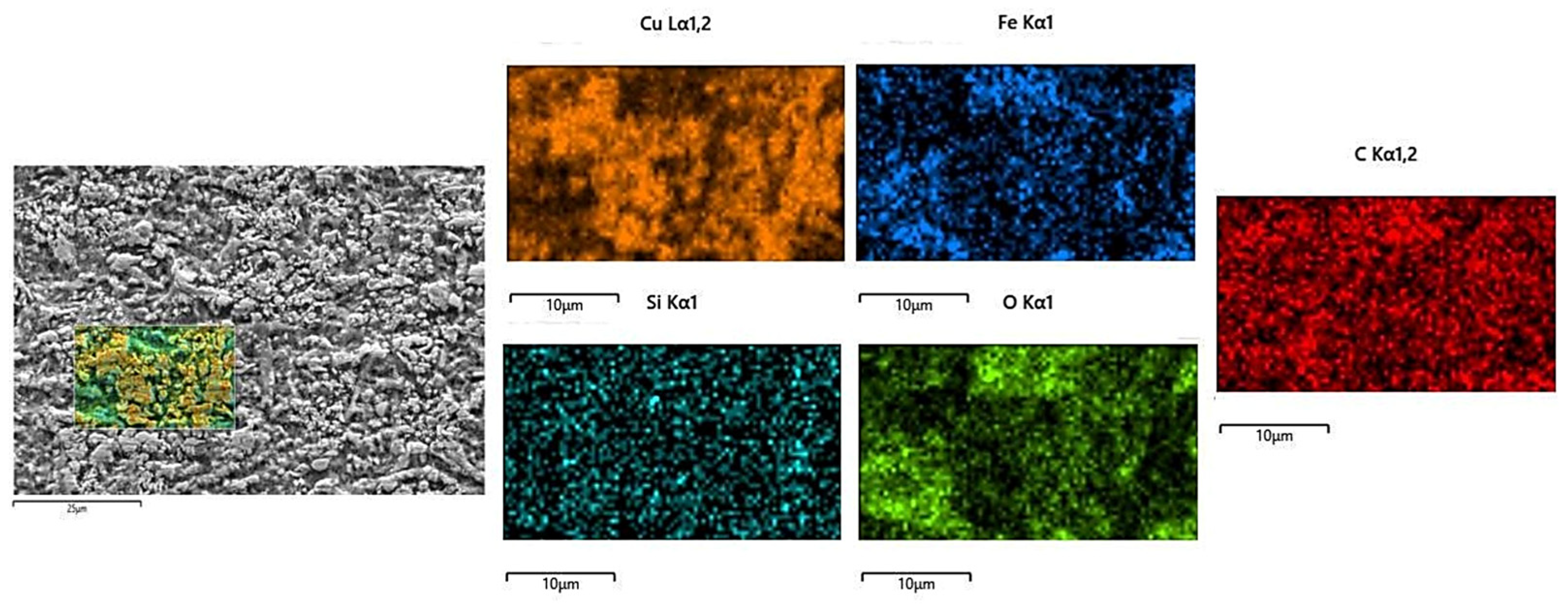
The microstructure evolution of the deposited layer is shown in Figure 8a–d. There are obvious dendrites in the microstructure [21]. The results show the presence of larger-sized iron oxides in S1. Figure 9 and Figure 10 reveal that the S4 deposited layer has finer dendrite morphology in the microstructure. In addition, the iron oxides in S4 are finer than those in S1. This phenomenon indicates that the increase in friction velocity refines the microstructure size of Cu-SiC deposited layer. In addition, there is Fe in the EDS results of the deposition. This phenomenon occurs because stainless steel is used as an anode. During the deposition process, Fe enters the deposition layer and turns into iron oxide. The presence of iron oxide was obvious in S1 and S2 deposited layers (see Figure 6). As the friction speed increased, the larger area of oxides disappeared. The reason for this phenomenon may be that as the friction speed increases, the friction force on the metal oxide with a larger area increases, thereby crushing the iron oxide with a larger area into small fragments. In addition, the elemental content of the microstructure of the deposited layer was tested by EDS, as shown in Table 3. As the friction speed increases, the content of Fe in the deposited layer gradually decreases. This phenomenon occurs because the Fe in the stainless steel rod enters the deposited layer during the friction process. However, friction and extrusion lead to the refinement of the microstructure, making it difficult for Fe elements to aggregate, resulting in a decrease in the Fe content in the deposited layer.
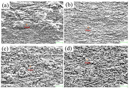
Figure 8.
Microstructure of electrodeposition layer: (a) S1 electrodeposition layer; (b) S2 electrodeposition layer; (c) S3 electrodeposition layer; (d) S4 electrodeposition layer.
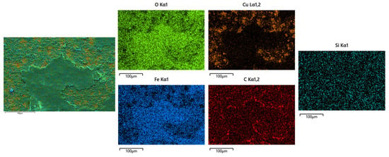
Figure 9.
EDS analysis of S1 electrodeposition layer.
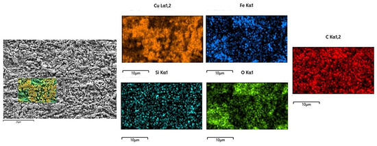
Figure 10.
EDS analysis of the S4 electrodeposition layer.
Table 3.
Chemical composition of electrodeposition layer (wt.%).
Therefore, it can be said that the friction speed has an important influence on the formation and microstructural characteristics of the deposited layer during the electrodeposition process. During the deposition process, Fe in the stainless steel anode dissolves and is deposited on the Cu substrate. Theoretically, the amount of anode dissolution and metal deposition directly depends on the amount of current passing through. According to Faraday’s law, it can be calculated using the following formula [22]:
where N is the deposition layer factor, I is the current between the electrode and the solution, and t is the deposition time.
In this study, the deposition layer factor and deposition time are constant values. According to Formula (2), the change in the morphology of the deposition layer is closely related to the current density. In other words, the friction speed changes the current between the electrode and the solution, thereby changing the morphology and microstructural characteristics of the electrodeposited layer. Related studies have also shown that the greater the current density, the finer the microstructure of the electrodeposited layer [23]. In the previous discussion, it was found that increasing the stirring speed during the electrodeposition process can increase the limiting current density of the cathode. Therefore, the reasons for the refinement of the S4 sample in this study come from two aspects. Firstly, under the action of friction, the increase in the current density of the deposition layer leads to an increase in the amount of stainless steel electrode dissolved in the deposition layer, which accelerates the dissolution of Fe into the deposition layer. Secondly, under the action of friction, the anode squeezes the SiC particles in the solution, making it easier for them to deposit on the Cu substrate. The embedding of the SiC particles disrupts the growth pattern of the deposition layer, causing areas where coarse grains might have formed to be refined into smaller grains. The SiC particles attached to the Cu matrix are squeezed against each other under the action of friction and are more easily broken into fine particles, which has an important influence on improving the mechanical properties of the deposited layer. In addition, the mechanical process and fluid dynamic factors in the friction-assisted electrodeposition process cannot be ignored. Specifically, SiC particles are transferred to the cathode surface by the moving fluid, and once they contact the cathode, they stay on it by external force. During the residence time, they are captured by the growing metal and embedded in the deposited layer. In this process, fluid dynamic factors have an important influence on the transfer and residence time of particles.
In addition, the dissolution of Fe in the electrolyte has an important influence on the performance of the deposited layer. In the previous discussion, it was found that the increase in friction speed will accelerate the entry of Fe into the deposited layer, which will lead to solid solution strengthening, thereby enhancing the mechanical properties of the deposited layer.
3.3. Microhardness
Figure 11 reveals the microhardness of the layers. The average microhardness of the S1–S4 deposited layers are 142.4, 154.0, 165.4, and 177.6 HV, respectively. The microhardness of the deposition is greater than that of the substrate. With the increase of friction speed, the microhardness of the deposition increases. The microhardness of the S4 sample increased by 24.7% compared with the S1 sample. This study found that the closer the deposited layer is to the substrate, the higher the microhardness.
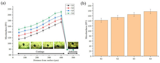
Figure 11.
Microhardness of the electrodeposition layer: (a) Microhardness curve; (b) Average microhardness.
This is consistent with the study of M. Shourgeshty et al. [24]. During the friction-assisted electrodeposition process, as the friction speed increases, more SiC particles at the interface participate in the deposition process and enter the Cu lattice, causing a greater degree of lattice distortion; the grains of different forms are more tightly combined; the number of holes in the composite deposition layer decreases; and the density gradually increases. Therefore, the composite deposition layer has an enhanced ability to withstand external load indentation and resist local plastic deformation, which is manifested as increased microhardness. Furthermore, the increase in microhardness of the deposited layer is inextricably linked to the refinement of the microstructure. It has been demonstrated that finer microstructure size has higher grain boundary density, which improves the strength and hardness of the deposited layer. According to the Hall–Petch criterion, the microhardness of the deposited layer can be improved as the grain size decreases [25]. Under the effect of friction, the microstructure of the deposited layer is more refined, which leads to an increase in the hardness of the deposited layer.
In other words, the improvement of the microhardness of the deposited layer by the friction effect is related to grain refinement and the interface characteristics of the deposited layer and the substrate. As analyzed in Figure 7, the increase in friction speed reduces the generation of voids in the deposited layer, which is beneficial for improving the microhardness of the deposited layer. Under the action of friction, more SiC particles are embedded in the deposited layer, which improves the hardness of the deposited layer to a certain extent. Therefore, under the action of friction, the improvement of the hardness of the deposited layer comes from many aspects, which are the refinement of the microstructure, the reduction of voids, and the increase in the amount of SiC embedded.
3.4. Anode Analysis
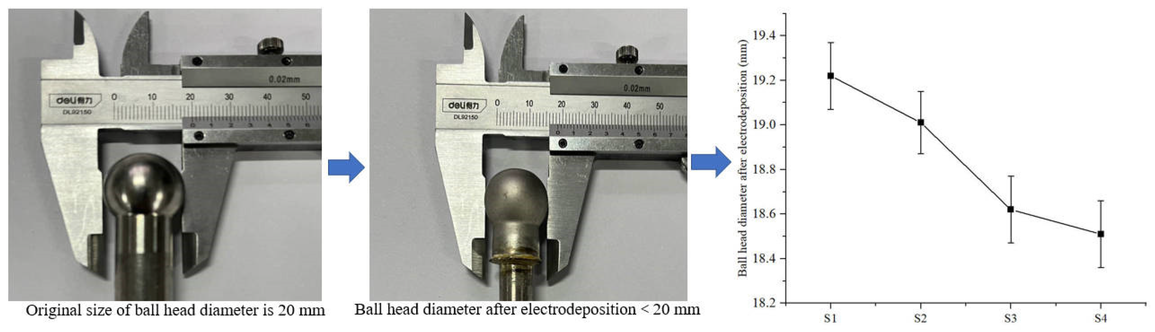
To further investigate the effect of friction on electrodeposition, the change in ball head size before and after electrodeposition was measured, as shown in Figure 12. The anode ball head size was 20 mm in diameter before electrodeposition, and the size after electrodeposition was less than 20 mm. The anode ball head sizes used for samples S1–S4 under friction were 19.22, 19.01, 18.62, 18.51mm. The ball head sizes decreased by 3.9%, 4.9%, 6.9%, and 7.5%, respectively, relative to the initial state. This indicates that as the friction velocity increases, the ball head size decreases. The reason for this phenomenon is related to the increase in current density under friction. The increase in current density accelerates the electrodeposition efficiency, which makes the metal ions in the anode accelerate into the solution and participate in the molding of the electrodeposited layer.
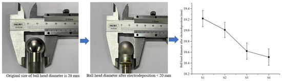
Figure 12.
Changes in the size of the anode ball head after electrodeposition.
However, the friction effect on the increase of current density affects the anode surface as well. Figure 13 shows the anode ball head surface morphology after electrodeposition. Many etch pits were found on the ball head morphology. In the electrodeposition process, the ball head, as the bulge part, has a high current density during the electrodeposition process, which makes the metal dissolve into the solution quickly. The friction effect leads to excessive current density in the localized area of the anode, and the surface layer of the specimen is damaged, generating bubble clusters on the surface that cannot escape from the surface, thus producing etch pits and pockmarks on the surface of the specimen [26,27]. Therefore, it is important to control the friction speed during friction-assisted electrodeposition to protect the anode.
3.5. Wear Properties
The friction coefficient (COF) curve and the average friction coefficient of the electrodeposited layer are shown in Figure 14. By observing the friction curve of the electrodeposited layer, it is found that with the increase of friction time, the friction coefficient of the electrodeposited layer increases with fluctuation and then tends to be stable. The reason for this phenomenon is that the resistance in the initial stage of friction is small. With the increase of friction time, the deposited layer undergoes plastic deformation under the action of cyclic load, and the wear debris gradually increases, which plays an obstructive role and increases the friction coefficient [28]. When the Si3N4 ball reaches a stable contact state with the friction surface, the friction coefficient region is stable. The average friction coefficients of the S1–S4 electrodeposited layers are 0.74, 0.69, 0.63, and 0.55, respectively. During the electrodeposition process, as the anode friction speed increases, the friction coefficient of the electrodeposited layer decreases. Compared with the S1 deposited layer, the COF of the S4 deposited layer decreases by 25.6%.
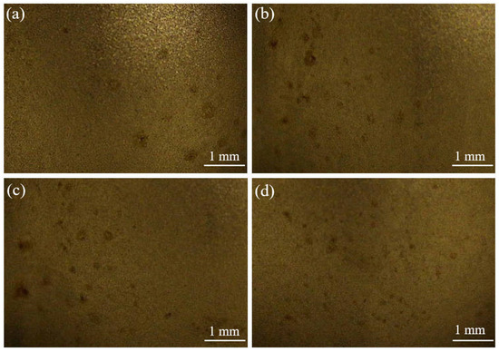
Figure 13.
Surface morphology of anode ball after electrodeposition: (a) S1 electrodeposition layer; (b) S2 electrodeposition layer; (c) S3 electrodeposition layer; (d) S4 electrodeposition layer.
Figure 13.
Surface morphology of anode ball after electrodeposition: (a) S1 electrodeposition layer; (b) S2 electrodeposition layer; (c) S3 electrodeposition layer; (d) S4 electrodeposition layer.
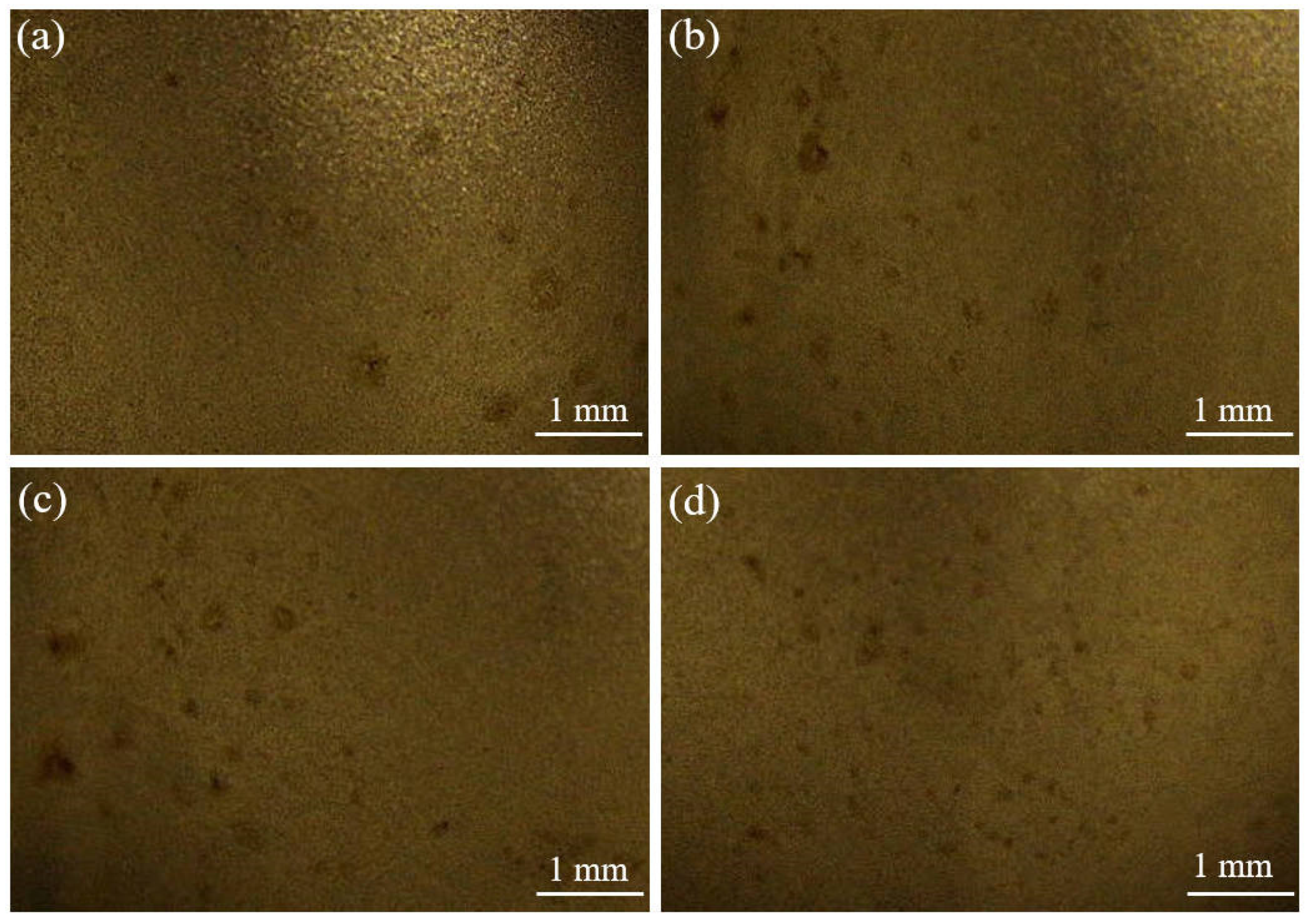
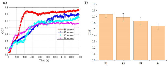
Figure 14.
COF of the electrodeposited layer: (a) COF curve; (b) Average COF values.
Figure 14.
COF of the electrodeposited layer: (a) COF curve; (b) Average COF values.

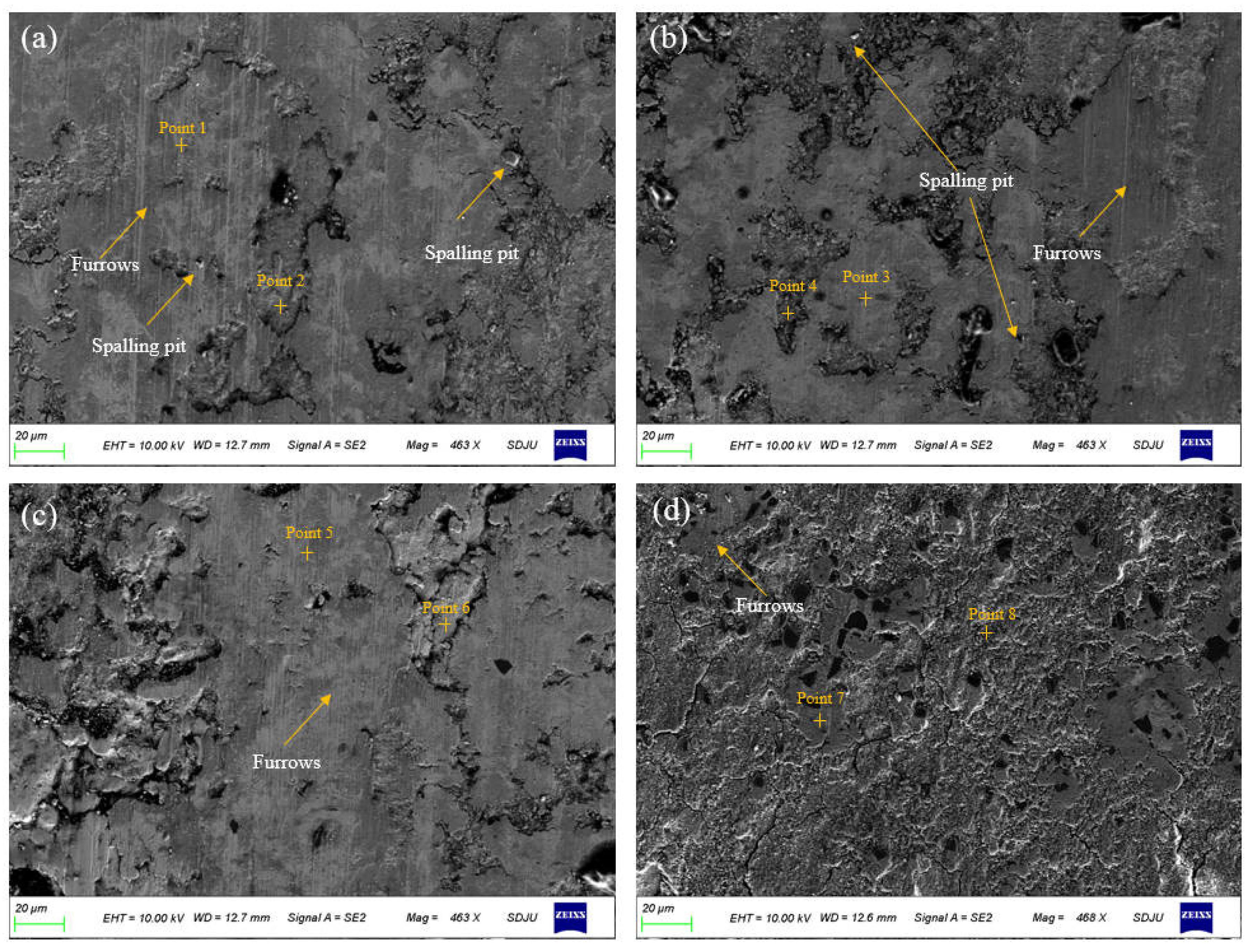
To further reveal the wear mechanism of the electrodeposited layer, the microscopic morphology of the worn samples was tested, as shown in Figure 15. The wear morphology reveals that the electrodeposited layer has different degrees of wear during the friction experiment. There are obvious spalling pits and plowing grooves in the wear morphology of the deposited layer. The spalling pits in the S1 and S2 deposited layers are more obvious. The presence of spalling pits can increase the friction coefficient during the friction process [29]. During the friction process, under the combined action of extrusion and plowing, the SiC particles in the deposited layer participate in the transfer of wear debris to the contact surface of the friction pair and delaminate and fracture under the action of mechanical shear force, and disperse on the contact surface to form a solid lubricating film, which can play a friction-reducing role, thereby reducing the friction coefficient of the composite deposition. The material transfer phenomenon appeared in the wear morphology of the deposited layer. EDS analysis was performed on different parts of the wear morphology (see Table 4). More Si elements were found in the EDS test of the material stacking part. This means that this part has a large distribution of SiC. The higher the SiC content in the composite electrodeposition layer, the more particles will naturally transfer and delaminate during the friction process, which will cause a larger area of solid lubrication film to form on the contact surface of the friction pair, which will effectively reduce friction and reduce the friction coefficient [30]. In addition, the density of the material in the composite electrodeposition layer also affects the friction coefficient. Since the material at the interface of the S4 deposition layer is smoother and denser, its ability to resist plastic deformation is enhanced, which also reduces the friction coefficient. Due to the low content of SiC particles at the interface of the S1 deposition layer, there are very few particles that are delaminated and fractured and transferred to the contact surface of the friction pair under the combined action of extrusion and plowing during the friction process, and the self-lubricating and friction-reducing effect is limited. In addition, the composite deposition formed when the SiC particle content is low has many crystal defects and a poor ability to resist local plastic deformation, which together lead to an increase in the friction coefficient of the S1 sample.
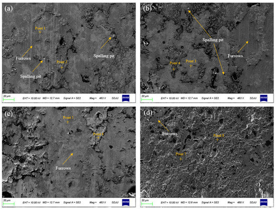
Figure 15.
Wear morphology of electrodeposited layers: (a) S1 electrodeposition layer; (b) S2 electrodeposition layer; (c) S3 electrodeposition layer; (d) S4 electrodeposition layer.
Table 4.
Elemental content of wear areas (wt.%).
The wear scar morphology of the laser-deposited layer was tested by optical microscopy, as shown in Figure 16. It can be seen from the figure that the wear scar width of the S1 deposited layer is the highest. Combined with the wear characteristics such as furrows and local peeling observed in Figure 15a, this shows that the surface wear of the S1 sample is more serious. The wear scar width of the S4 deposit layer is reduced by about 21.2% compared with that of the S1 deposit layer.
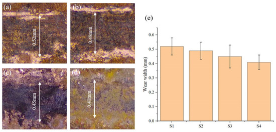
Figure 16.
Wear width of electrodeposited layers: (a) S1 electrodeposition layer; (b) S2 electrodeposition layer; (c) S3 electrodeposition layer; (d) S4 electrodeposition layer; (e) Average wear width of the electrodeposition layers.
As shown in Figure 15, wear features such as furrows and local peeling can be observed on the wear surface of the S1 and S2 deposit layers, and the edge is accompanied by wear debris accumulation. This shows that the wear degree of the deposit layer surface is serious. The reason is that the deposited layer has low microhardness and poor wear resistance. It is easy to cause adhesive wear and abrasive wear during the friction process. At the same time, furrows are formed under the action of extrusion and plowing, accompanied by local peeling [31]. As shown in Figure 15c,d, as the friction speed increases during the electrodeposition process, the peeling pit phenomenon formed on the surface of the composite deposit layer gradually disappears. This is related to the different content of SiC particles in the composite deposit layer and the difference in the self-lubricating and friction-reducing effect of the particles during the friction process. During the friction process, hardness also has an important influence on the friction coefficient of the electrodeposited layer. The increase in hardness, the resistance to local plastic deformation, and wear resistance are enhanced, thereby reducing the friction coefficient and wear width of the composite electrodeposited layers.
4. Conclusions
In this study, a friction-assisted electrodeposition method was used to successfully prepare Cu-SiC composite deposition on a copper substrate. The study found that the friction effect leads to a finer microstructure of the deposited layer. During the friction-assisted electrodeposition process, the size of the anode stainless steel rod is reduced, and the Fe element enters the deposited layer, which has an important impact on the performance of the deposited layer. The increase in friction speed leads to an increase in SiC content in the deposited layer and a decrease in defects at the interface. The morphology, microstructure, and wear properties of the deposited layer were studied. It was found that as the friction speed increased, the width of the deposition increased by up to 68.7%. The microstructure of the deposited layer is mainly composed of dendrites. As the friction speed increases to 40 mm/s, the hardness of the deposition can reach 177.6 HV, which is increased by 24.7% compared with the low friction speed. Meanwhile, it was found that as the friction speed increases, the metal oxides with larger areas are broken into fine fragments under the friction effect. Under the influence of the friction effect, the wear resistance of the deposited layer was improved, the wear width was reduced by 21.2%, and the friction coefficient was reduced by 25.6%. However, the electrochemical properties and the mechanism of friction-assisted composite electrodeposition on material migration are still unclear and need further study.
Author Contributions
K.Q.: Conceptualization, investigation, methodology, writing original draft, measurements, and validating the results; K.L.: Investigation and experiment analysis; Y.Y.: investigation and measurements; Q.S.: Resources and experiments; X.Y.: Resources and experiments; L.J.: Experimental analysis, review, and editing. All authors have read and agreed to the published version of the manuscript.
Funding
This research was funded by Shandong Provincial Natural Science Foundation, grant number [ZR2023QE084].
Data Availability Statement
The original contributions presented in this study are included in the article. Further inquiries can be directed to the corresponding author.
Conflicts of Interest
Youliang Yu and Qinpeng Sun were employed by the Haihui Group Co., Ltd. The remaining authors declare that the research was conducted in the absence of any commercial or financial relationships that could be construed as a potential conflict of interest.
References
- Li, X.; Ming, P.; Ao, S.; Wang, W. Review of additive electrochemical micro-manufacturing technology. Int. J. Mach. Tools Manuf. 2022, 173, 103848. [Google Scholar] [CrossRef]
- Srivastava, M.; Grips, V.K.W.; Rajam, K.S. Electrochemical deposition and tribological behaviour of Ni and Ni–Co metal matrix composites with SiC nano-particles. Appl. Surf. Sci. 2007, 253, 3814–3824. [Google Scholar] [CrossRef]
- Datta, M. Manufacturing processes for fabrication of flip-chip micro-bumps used in microelectronic packaging: An overview. J. Micromanufacturing 2020, 3, 69–83. [Google Scholar] [CrossRef]
- Raghavendra, C.R.; Basavarajappa, S.; Sogalad, I. Electrodeposition of Ni-nano composite coatings: A review. Inorg. Nano-Met. Chem. 2018, 48, 583–598. [Google Scholar] [CrossRef]
- Kumar, V.; Singh, A.; Ankit; Gautam, G. A comprehensive review of processing techniques, reinforcement effects, and performance characteristics in copper-based metal matrix composites. Interactions 2024, 245, 357. [Google Scholar] [CrossRef]
- Xu, X.; Du, J.L.; Luo, K.Y.; Peng, M.X.; Xing, F.; Wu, L.J.; Lu, J.Z. Microstructural features and corrosion behavior of Fe-based coatings prepared by an integrated process of extreme high-speed laser additive manufacturing. Surf. Coat. Technol. 2021, 422, 127500. [Google Scholar] [CrossRef]
- Cardoso, R.M.; Kalinke, C.; Rocha, R.G.; Dos Santos, P.L.; Rocha, D.P.; Oliveira, P.R.; Janegitz, B.C.; Bonacin, J.A.; Richter, E.M.; Munoz, R.A. Additive-manufactured (3D-printed) electrochemical sensors: A critical review. Anal. Chim. Acta 2020, 1118, 73–91. [Google Scholar] [CrossRef]
- Siddiqui, H.; Singh, N.; Naidu, P.; Rao, K.B.S.; Gupta, S.; Srivastava, A.K.; Santosh, M.S.; Natarajan, S.; Kumar, S.; Dumée, L.F.; et al. Emerging electrochemical additive manufacturing technology for advanced materials: Structures and applications. Mater. Today 2023, 70, 161–192. [Google Scholar] [CrossRef]
- Ayalew, A.A.; Han, X.; Sakairi, M. A critical review of additive material manufacturing through electrochemical deposition techniques. Addit. Manuf. 2023, 77, 103796. [Google Scholar] [CrossRef]
- Van Nisselroy, C.; Shen, C.; Zambelli, T.; Momotenko, D. Electrochemical 3D printing of silver and nickel microstructures with FluidFM. Addit. Manuf. 2022, 53, 102718. [Google Scholar] [CrossRef]
- Xu, J.; Ren, W.; Lian, Z.; Yu, P.; Yu, H. A review: Development of the maskless localized electrochemical deposition technology. Int. J. Adv. Manuf. Technol. 2020, 110, 1731–1757. [Google Scholar] [CrossRef]
- Volgin, V.M.; Kabanova, T.B.; Davydov, A.D. Modeling of local maskless electrochemical deposition of metal microcolumns. Chem. Eng. Sci. 2018, 183, 123–135. [Google Scholar] [CrossRef]
- Biswal, H.J.; Kaur, J.J.; Vundavilli, P.R.; Gupta, A. Recent advances in energy field assisted hybrid electrodeposition and electroforming processes. CIRP J. Manuf. Sci. Technol. 2022, 38, 518–546. [Google Scholar] [CrossRef]
- Grishko, V.I.; Duley, W.W.; Gu, Z.H.; Fahidy, T.Z. Laser-assisted electrochemical deposition on certain cathodes. Electrochim. Acta 2001, 47, 643–650. [Google Scholar] [CrossRef]
- Zhang, Z.; Wu, Y.; Wang, A.; Xu, K.; Dai, X.; Zhu, H.; Yang, S. A study on laser enhanced electrodeposition for preparation Fe-Ni alloy. Materials 2020, 13, 3560. [Google Scholar] [CrossRef]
- Peng, J.; Yu, J.; Chu, D.; Hou, X.; Jia, X.; Meng, B.; Yang, K.; Zhao, J.; Yang, N.; Wu, J.; et al. Synergistic effects of an artificial carbon coating layer and Cu2+-electrolyte additive for high-performance zinc-based hybrid supercapacitors. Carbon 2022, 198, 34–45. [Google Scholar] [CrossRef]
- Fan, H.J.; Knez, M.; Scholz, R.; Hesse, D.; Nielsch, K.; Zacharias, M.; Gösele, U. Influence of surface diffusion on the formation of hollow nanostructures induced by the Kirkendall effect: The basic concept. Nano Lett. 2007, 7, 993–997. [Google Scholar] [CrossRef]
- Lee, J.L.; Shih, Y.S. Applicability of the Levich Equation for a Two-Phase Solution in the Rotating Disk Electrode System. J. Chin. Chem. Soc. 1990, 37, 265–271. [Google Scholar] [CrossRef]
- Turner, D.R.; Johnson, G.R. The effect of some addition agents on the kinetics of copper electrodeposition from a sulfate solution: I. Cathode potential-current density relation. J. Electrochem. Soc. 1962, 109, 798. [Google Scholar] [CrossRef]
- Qu, N.S.; Zhu, D.; Chan, K.C.; Lei, W.N. Pulse electrodeposition of nanocrystalline nickel using ultra narrow pulse width and high peak current density. Surf. Coat. Technol. 2003, 168, 123–128. [Google Scholar] [CrossRef]
- Sharma, A.; Bhattacharya, S.; Das, S.; Das, K. A study on the effect of pulse electrodeposition parameters on the morphology of pure tin coatings. Metall. Mater. Trans. A 2014, 45, 4610–4622. [Google Scholar] [CrossRef]
- Rai, P.K.; Gupta, A. Investigation of surface characteristics and effect of electrodeposition parameters on nickel-based composite coating. Mater. Today: Proc. 2021, 44, 1079–1085. [Google Scholar] [CrossRef]
- Yuan, X.; Wang, Y.; Sun, D.; Yu, H. Influence of pulse parameters on the microstructure and microhardness of nickel electrodeposits. Surf. Coat. Technol. 2008, 202, 1895–1903. [Google Scholar]
- Shourgeshty, M.; Aliofkhazraei, M.; Karimzadeh, A. Study on functionally graded Zn–Ni–Al2O3 coatings fabricated by pulse-electrodeposition. Surf. Eng. 2019, 35, 167–176. [Google Scholar] [CrossRef]
- Han, J.; Wu, Y.; Zhao, K.; Wang, H.; Liu, S.; Liu, X. Effects of controlling grain growth mode on microstructures and properties of Cu foil. J. Mater. Res. Technol. 2023, 24, 2018–2027. [Google Scholar] [CrossRef]
- Lehmann, V. The physics of macropore formation in low doped n-type silicon. J. Electrochem. Soc. 1993, 140, 2836. [Google Scholar] [CrossRef]
- Durmus, Y.E.; Guerrero, S.S.M.; Aslanbas, Ö.; Tempel, H.; Hausen, F.; De Haart, L.G.J.; Ein-Eli, Y.; Eichel, R.A.; Kungl, H. Investigation of the corrosion behavior of highly As-doped crystalline Si in alkaline Si–air batteries. Electrochim. Acta 2018, 265, 292–302. [Google Scholar] [CrossRef]
- Liu, B.; Chen, H.; Zhou, J.; Wang, J.; Wang, W.; Chen, X.; Xi, S. Investigation of phase transition, tribological behavior and wear mechanisms of WC-enhanced biphase eutectic high entropy alloy by fast hot pressing sintering. Tribol. Int. 2024, 191, 109065. [Google Scholar] [CrossRef]
- Li, C.; Deng, X.; Wang, Z. Friction behaviour and self-lubricating mechanism of low alloy martensitic steel during reciprocating sliding. Wear 2021, 482, 203972. [Google Scholar] [CrossRef]
- Hu, T.; Hu, L.; Ding, Q. Effective solution for the tribological problems of Ti-6Al-4V: Combination of laser surface texturing and solid lubricant film. Surf. Coat. Technol. 2012, 206, 5060–5066. [Google Scholar] [CrossRef]
- Zhang, X.; Zhang, T.; Chen, K.; Xu, H.; Feng, C.; Zhang, D. Wear mechanism and debris analysis of PEEK as an alternative to CoCrMo in the femoral component of total knee replacement. Friction 2023, 11, 1845–1861. [Google Scholar] [CrossRef]


Disclaimer/Publisher’s Note: The statements, opinions and data contained in all publications are solely those of the individual author(s) and contributor(s) and not of MDPI and/or the editor(s). MDPI and/or the editor(s) disclaim responsibility for any injury to people or property resulting from any ideas, methods, instructions or products referred to in the content. |
© 2025 by the authors. Licensee MDPI, Basel, Switzerland. This article is an open access article distributed under the terms and conditions of the Creative Commons Attribution (CC BY) license (https://creativecommons.org/licenses/by/4.0/).