Abstract
In this study, we investigated and compared the influence of alumina nanoparticles (Al-NPs) and silicon nitride (SiNx) layers individually deposited on multi-crystalline silicon (mc-Si) on mc-Si’s structural, optical, and optoelectronic characteristics to improve surface quality. Alumina nanoparticle-covered multi-crystalline silicon, immersion in HF/H2O2/HNO3, and porous silicon (PS) covered with a silicon nitride structure are key components in achieving high electronic quality in multi-crystalline silicon. Surface reflectivity decreased from 27% to a minimum value of 2% for alumina nanoparticles/PS and a minimum value of 5% for silicon nitride/PS at a wavelength of 930 nm. Meanwhile, the minority carrier diffusion length increased from 2 µm to 300 µm for porous silicon combined with silicon nitride and to 100 µm for alumina nanoparticles/porous silicon. Two-dimensional current mapping further demonstrated a considerable enhancement in the generated current, rising from 2.8 nA for untreated mc-Si to 34 nA for Al-NPs/PS and 66 nA for PS/SiNx. These results confirm that the surface passivation of mc-Si using Al-NPs or PS combined with SiNx is a promising and efficient method to improve the electrical quality of mc-Si wafers, contributing to the development of high-performance mc-Si-based solar cells.
1. Introduction
Multi-crystalline silicon (mc-Si) is a prevalent material in solar cell production due to its cost-effectiveness and reasonable efficiency [1,2]. However, its electronic quality often suffers from defects, impurities, and grain boundaries, limiting its performance [3,4,5]. Recent studies have explored the use of silicon nitride [6] and alumina nanoparticles [7] to enhance the electronic properties of mc-Si. Multi-crystalline silicon comprises multiple silicon crystals, leading to a heterogeneous structure that can negatively impact charge carrier mobility and recombination rates. Defects in mc-Si, such as dislocations and grain boundaries [8,9], are known to act as recombination centers, reducing overall efficiency. Silicon nitride is widely used as a passivation layer in solar cells due to its excellent dielectric properties and ability to reduce surface recombination. The incorporation of silicon nitride (SiNx) and alumina nanoparticles (Al-NPs) [10] creates a barrier that prevents minority carrier recombination at the silicon’s surface, thus enhancing charge carrier lifetime. Lowering the surface reflectance of silicon wafers through porous silicon (PS) [11,12] treatment is a key process for enhancing the efficiency of silicon solar cells. The formation of PS via stain etching (SE) [13] is a suitable approach for the photovoltaic industry, as it requires only a short immersion of the substrates in the appropriate solution [13]. In a previous study, we reported that SE of the silicon substrate led to a significant reduction in surface reflectance [14]. This is of great importance for silicon-based solar cells due to the improvement of sunlight absorption. On the other hand, alumina nanoparticle/PS and silicon nitride (SiNx)/PS combinations could act not only as an antireflection coating (ARC), but also improve the performance of photovoltaic devices by defect, surface, and bulk passivation. A simple, low-cost, and scalable method was used to form aluminum nanoparticles (Al-NPs) on the mc-Si surface. Additionally, the optoelectronic properties were experimentally characterized through direct measurements, offering more reliable insights into the effectiveness of the proposed surface treatment, in contrast to previous studies [6,7]. This study aims to demonstrate the enhancement of surface passivation and electronic quality in mc-Si through the use of aluminum/porous silicon nanostructures and PS combined with SiNx. Al-NP-covered mc-Si immersed in HF/H2O2/HNO3 and mc-Si immersed in HF/H2O2/HNO3 covered with silicon nitride deposited by plasma-enhanced chemical vapor deposition (PECVD) were characterized to investigate the optic and optoelectronic properties of their structures by measuring reflectance, IR absorption, lifetime, and laser beam-induced current (LBIC).
2. Materials and Methods
A p-type mc-Si wafer with a thickness of 350 µm and a resistivity of 2.0–0.5 Ω cm was used in this work. Porous silicon layers (PS) were created by a stain etching (SE) method at room temperature using a mixed solution containing H2O:HNO3:HF at a ratio of 5:3:1. The solution was agitated to prevent H2 from bubbling over the etching surface, thus fabricating a more uniform PS structure. An aluminum layer with a thickness of a few micrometers was deposited onto the mc-Si surface, followed by thermal annealing at 550 °C for 15 min to promote Al diffusion into the grains and along grain boundaries, thereby enhancing surface passivation. After annealing, the samples were chemically etched using a CP4 acidic solution to selectively remove the residual aluminum. This process led to the formation of isolated Al-NPs with an average diameter of ~100 nm that were uniformly distributed over the mc-Si surface. The sample with alumina nanoparticles was treated in HF:HNO3:H2O solution for a few seconds to obtain the silicon nanostructures, while the mc-Si treated in HF:HNO3:H2O solution was covered with a silicon nitride (SiNx) thin film using a Plasma-Enhanced Chemical Vapor Deposition (PECVD) by decomposition of silane SiH4 and H2. The samples’ surface structures were observed by a scanning electron microscope (JEOL JSM-5400, Tokyo, Japan). UV–vis–NIR spectrophotometer (Perkin-Elmer Lambda 950, Springfield, IL, USA) equipment measured reflectance with an integrating sphere in the 250–1200 nm wavelength range. Fourier transform infrared (Nicolet MAGNA-IR 560 ESP FT-IR, Madison, WI, USA) analysis was used to estimate bond densities in the elaborated samples. The minority carriers’ diffusion length was determined by the Homemade Light Beam-Induced Current (LBIC) measurement system to quantify the electronic quality of the treated mc-Si.
3. Results and Discussion
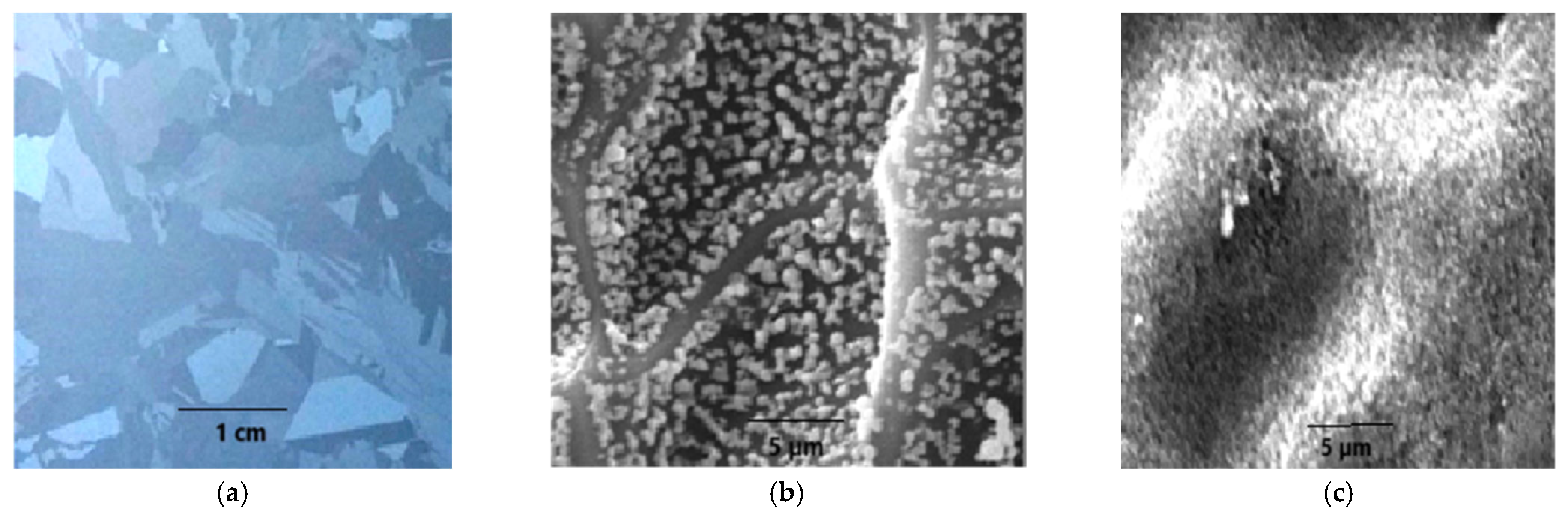
Figure 1 shows the SEM surface structure of mc-Si. The top-view SEM images provided valuable insights into the structural features, grain boundaries (GBs), and surface conditions that influenced the electronic properties of mc-Si, which are critical for solar cell applications.
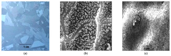
Figure 1.
SEM morphology of mc-S: (a) Ref mc-Si wafer (b) Al-NP dispersion (c) Al-NP-coated mc-Si treated with PS.
The SEM micrographs of bare mc-Si revealed a mosaic-like structure characterized by distinct grains of varying sizes (Figure 1a). The grain sizes significantly affected the electronic properties of mc-Si. Larger grains generally led to improved charge carrier mobility and reduced recombination rates. Variability in grain size indicates the quality of the crystallization process during manufacturing. Uniform grain sizes are often associated with higher-quality material. Figure 1a shows varying degrees of surface roughness, which is influenced by fabrication methods and the subsequent texturing processes. The increased surface roughness enhanced light absorption by reducing reflectivity, which is beneficial for solar cell efficiency. However, excessive roughness may lead to increased defect densities and surface states, potentially harming electronic performance. The grain boundaries were visible, appearing as lines or interfaces separating different crystalline regions. These boundaries act as recombination centers for charge carriers, negatively affecting the efficiency of mc-Si solar cells. Understanding the distribution and characteristics of grain boundaries is crucial for improving the electronic quality of the material. Figure 1b shows alumina nanoparticle dispersion on a mc-Si surface. SEM images provided crucial insights into the dispersion, morphology, and interactions of aluminum nanoparticles with the mc-Si surface. The results obtained revealed the distribution pattern of aluminum nanoparticles across the mc-Si surface. A uniform dispersion of nanoparticles is desirable, as it can enhance the optical and electrical properties of mc-Si. Clusters or agglomerations of nanoparticles may indicate issues during the deposition process, potentially leading to uneven light scattering and localized recombination sites. An even distribution can improve light trapping and enhance the overall absorption efficiency of a solar cell.
The SEM images showed the size, shape, and morphology of the aluminum nanoparticles. The successful integration of aluminum nanoparticles led to improved surface passivation, reducing surface recombination rates of charge carriers. The interface between the nanoparticles and the mc-Si surface is critical. Effective bonding enhances charge carrier collection, while weak interactions may lead to increased recombination. Aluminum nanoparticles enhance light trapping through scattering and absorption mechanisms, which may not be directly visible in SEM images, but can be inferred from the dispersion quality and morphology. Figure 1c shows the mc-Si-covered Al nanoparticles after HF/H2O2/HNO3 treatment. The SEM images provid critical insights into the morphological changes and dispersions of aluminum nanoparticles on the mc-Si surface after such treatments. The HF treatment effectively removed native silicon oxide layers, resulting in a cleaner silicon surface that may have enhanced the adhesion of aluminum nanoparticles.
The subsequent H2O2 and HNO3 treatments oxidized the aluminum nanoparticles, potentially altering their size and morphology, leading to more uniform dispersions. The chemical treatments not only modified the nanoparticles, but also affected the mc-Si surface itself, potentially increasing surface area and improving light trapping. Enhanced surface passivation may result from the interaction between aluminum nanoparticles and the silicon surface, reducing recombination rates and improving charge carrier dynamics. The combination of cleaning and nanoparticle dispersion is likely to enhance the effective utilization of incident light, which is essential for improving the efficiency of solar cells.
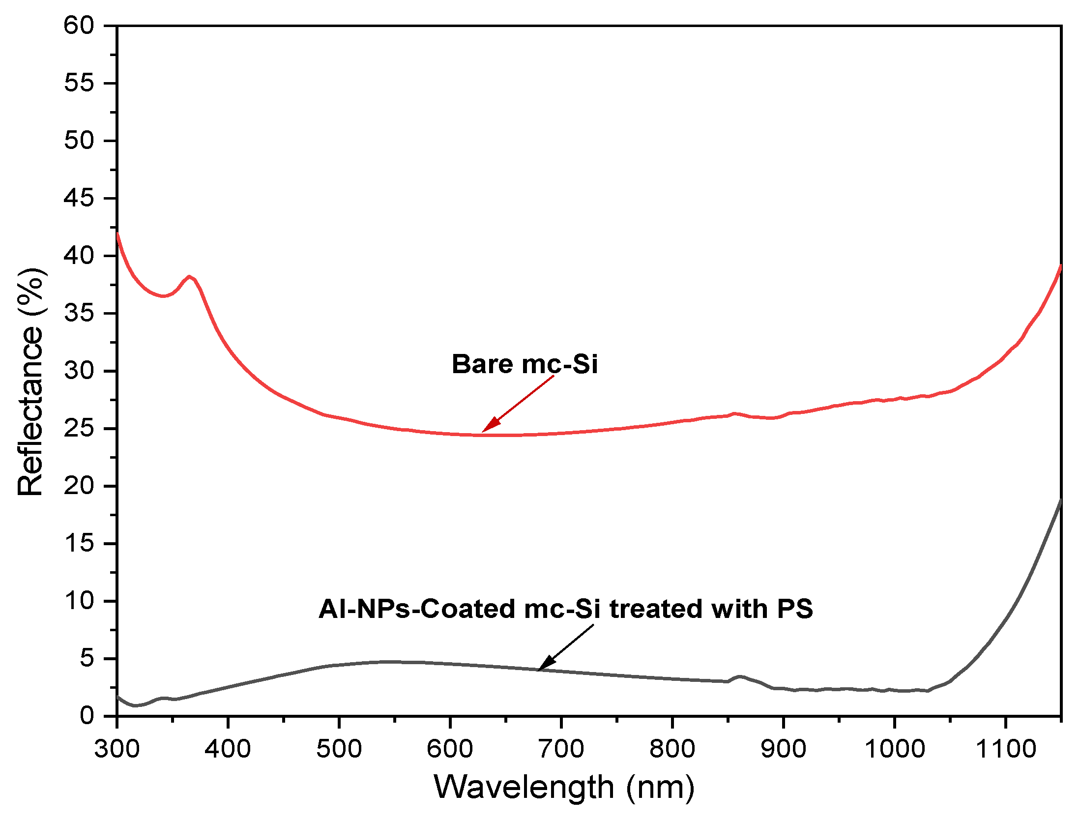
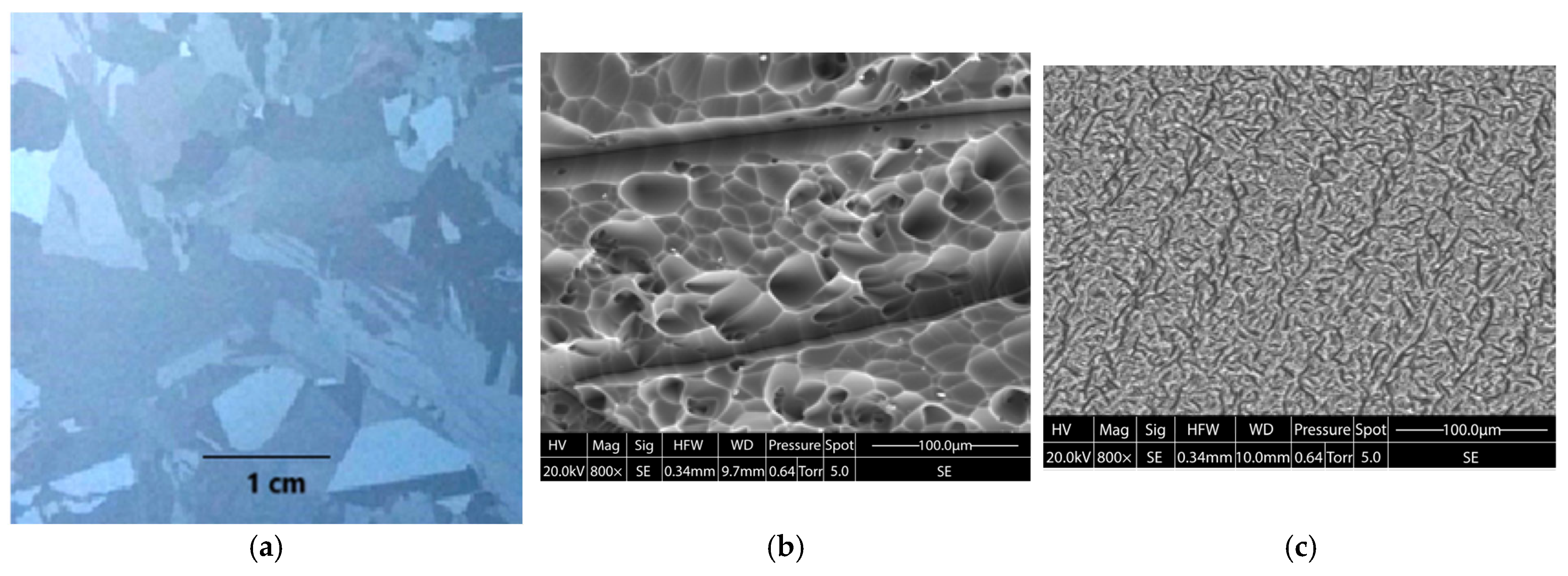
The surface reflectance of mc-Si with and without Al-NPs treated with PS are shown in Figure 2. From the reflectivity spectra, it is clear that the average reflectivity of Al-NPs treated by PS in the 300–1200 nm range was significantly lower than that of the bare mc-Si sample. The reflectivity of the silicon surface decreased to below 4% for most wavelengths in the spectrum (450–1050 nm) and further dropped to 2% in the lower wavelength range (300–450 nm). This indicates that the silicon nanostructures (Ns) formed after Al-NPs were treated with PS enhanced light absorption, with the lowest reflectivity attributed to the formation of mc-Si nanostructures that were suitable for light trapping due to multiple reflections [15,16,17,18]. It is well-known that mc-Si-Ns mainly absorb short-wavelength incident light. The SEM morphology shown in Figure 1c confirms the existence of nanostructures formed by pores of varying dimensions and supports the light trapping structure observed in Figure 2, as indicated by the reduction in reflectivity, as suggested by [19]. Figure 3 shows a typical SEM micrograph (top view) of PS covered with silicon nitride. The top-view SEM images revealed the porous structure of the silicon as characterized by a network of interconnected pores. The morphology of PS is crucial, as it influences light trapping and overall optical properties. Its highly porous structure enhanced light absorption via scattering effects. The modification of the PS surface with SiNx resulted in changes in reflectivity and light absorption characteristics, which may not be directly visible in SEM, but can be inferred from morphology. The SiNx layer enhanced the optical properties of PS by reducing surface reflectance and improving light absorption. Understanding the interaction between the SiNx layer and the porous structure helps in designing devices with optimized light management properties.
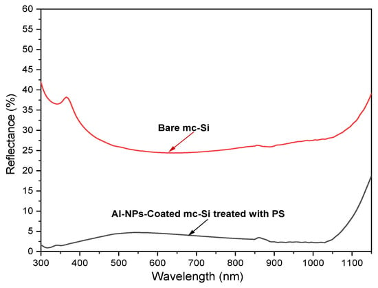
Figure 2.
Total reflectance before and after silicon nanostructure formation.
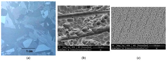
Figure 3.
SEM image of mc-Si (a) ref sample (b) PS and (c) PS covered with SiNx.
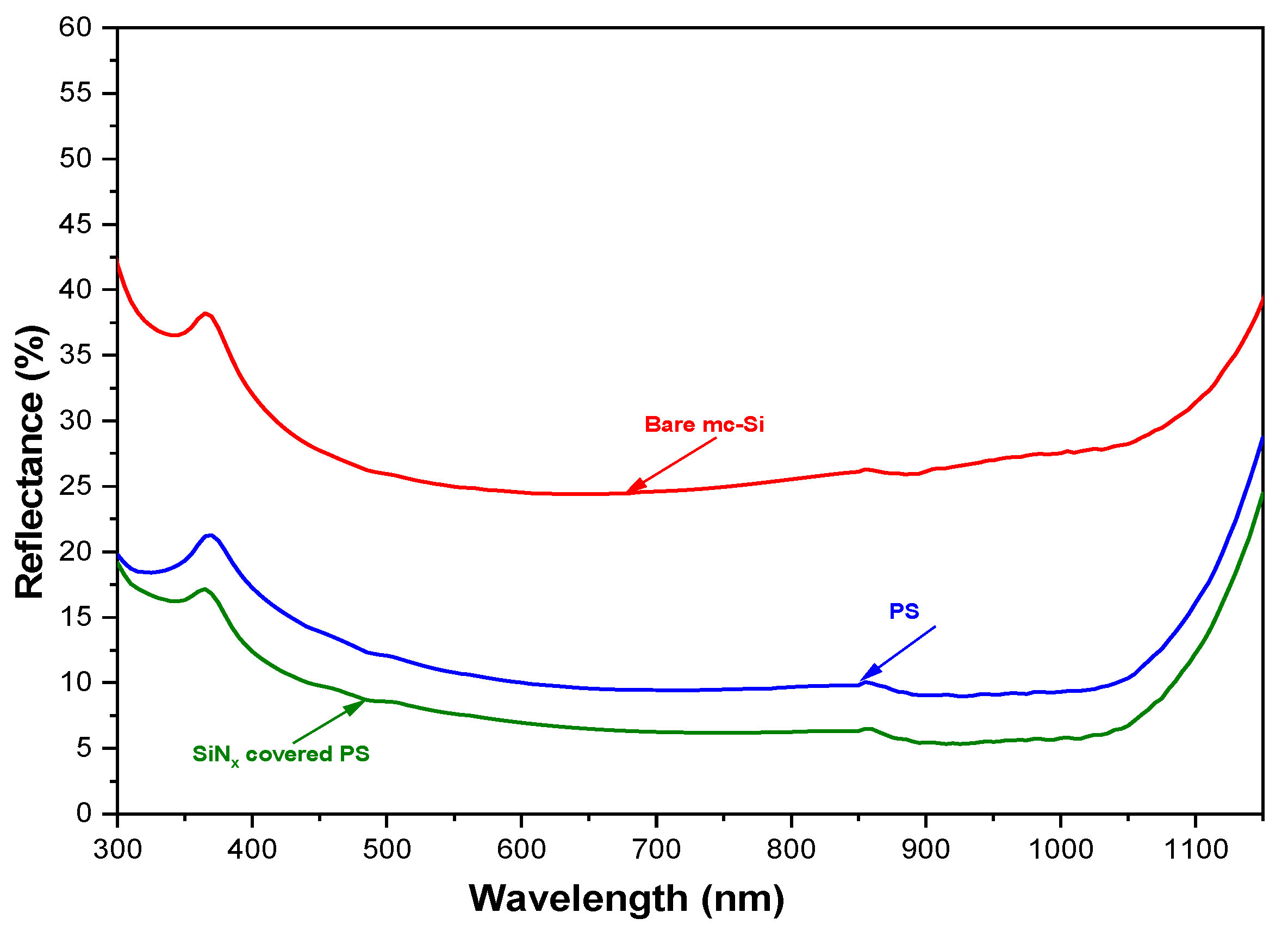
The surface morphology was homogeneous and exhibited an irregular structure that may have been suitable for light trapping and diffusion. The optical reflectivity of this structure, compared to both untreated and PS-treated mc-Si, decreased dramatically to about 5% at a wavelength of 930 nm (Figure 4). This can be explained, as previously reported [16], by the increase in surface roughness.
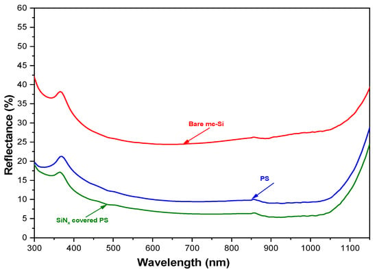
Figure 4.
Reflectivity characteristics of mc-Si: Bare, treated PS, and treated PS covered by SiNx layer.
A comparison of mc-Si-treated PS and mc-Si-treated PS covered by SiNx shows some benefits. First, mc-Si-treated PS covered by SiNx was formed homogeneously on the entire area of the mc-Si surface without obstruction of the grain orientation. Second, mc-Si-treated PS covered by SiNx demonstrated optical absorption greater than the mc-Si-treated PS layers. Also, PS and SiNx had some passivating capabilities that could allow the fabrication of solar cells without an additional passivation coating.
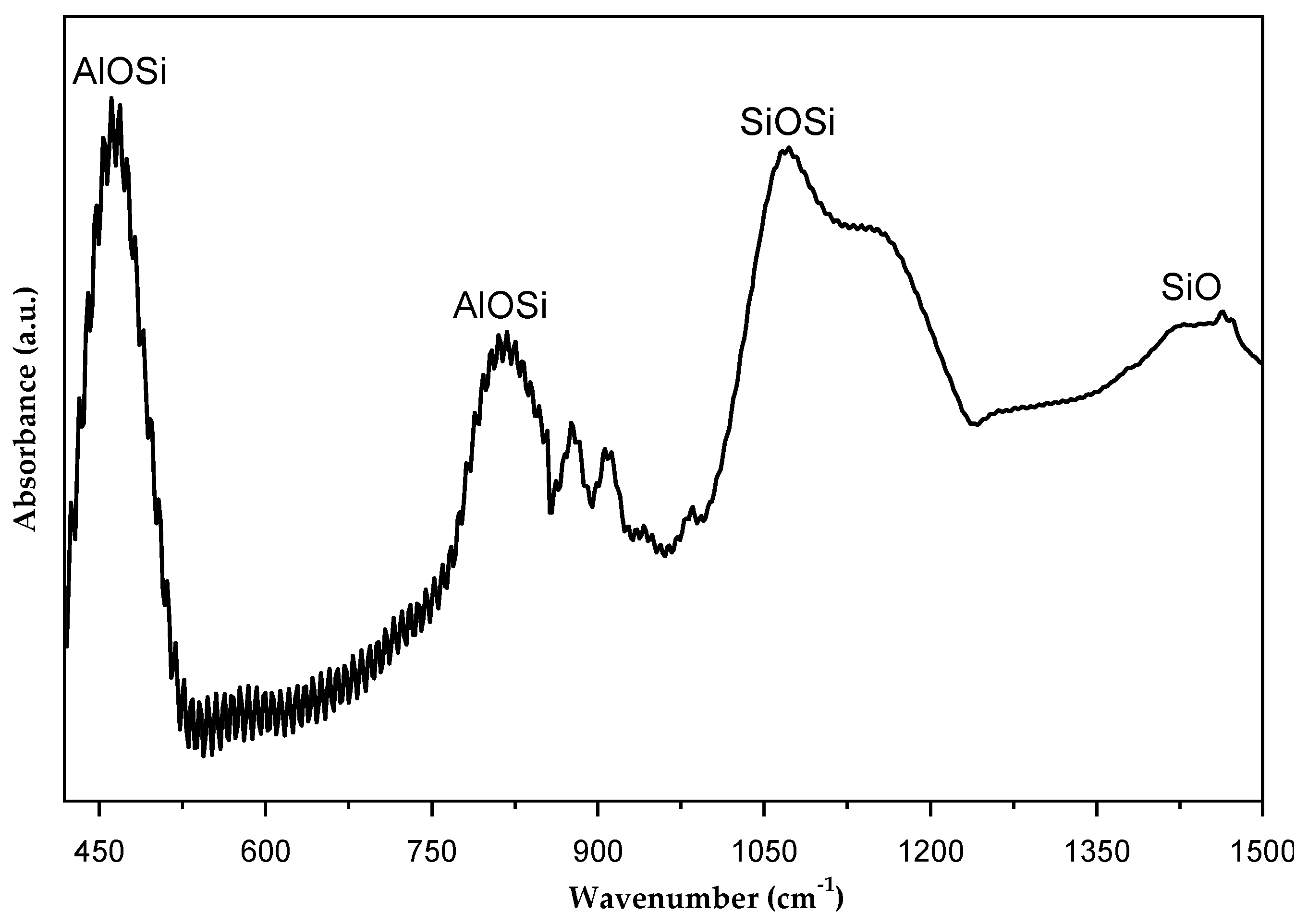
To quantify the electronic quality of mc-Si substrates treated with PS-covered SiNx and alumina nanoparticles, their optoelectronic properties were studied using two methods: diffusion length and produced current surface distribution. The diffusion length of alumina nanoparticle-covered mc-Si, as measured [20,21], increased drastically from 2 µm for the bare sample to 100 µm for Al-NPs treated by PS. This significant increase suggests that enhanced diffusion length and improved surface quality could primarily be attributed to the passivation effect of the Al-oxide species and the reduction in surface recombination velocity, likely due to aluminum gettering [22] (during annealing, aluminum diffuses and penetrates the mc-Si, thereby removing impurities/defects), which was confirmed by FT-IR characterization, as shown in Figure 5.
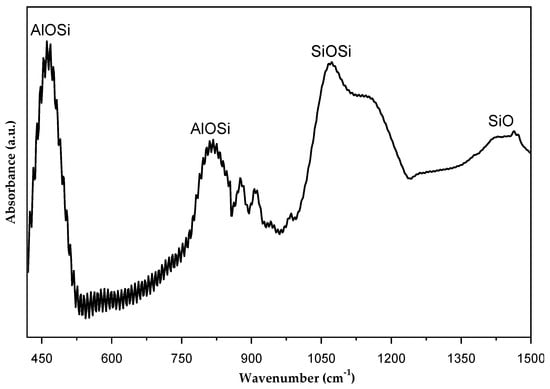
Figure 5.
FT-IR characterization of Al-NP-treated PS.
As shown in Figure 5, the peaks at 810 and 460 cm−1 were attributed to the stretching mode of Al-O-Si [19]. Notably, these peaks aligned well with those reported in previous literature [23,24,25,26,27,28]. The SiO and Al-O-Si species generated by Al-NPs treated with PS structures helped passivate the defects and dangling bonds at the interface and grain boundaries (GBs) of multi-crystalline silicon samples. In contrast, for PS covered with SiNx, the diffusion length of minority carriers increased from 2 µm in bare mc-Si to 300 µm in PS-covered SiNx. This improvement is attributed to the passivation of defects in mc-Si by the penetrated hydrogen, leading to an overall enhancement in the quality of mc-Si for solar cell applications, as confirmed by FT-IR characterization, shown in Figure 6.
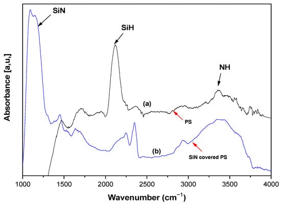
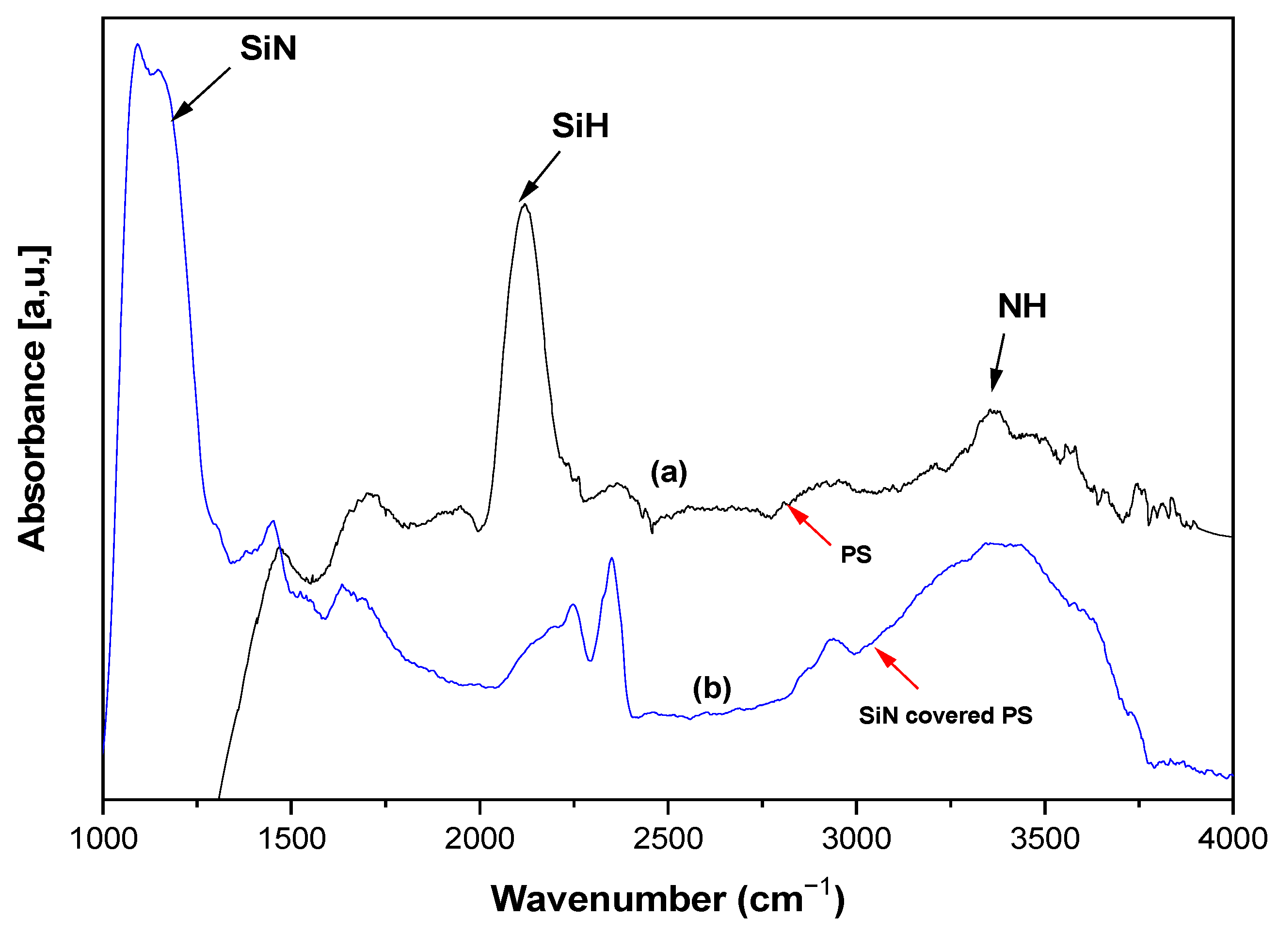
Figure 6.
FT-IR characterization of mc-Si-treated PS (a) without and (b) with SiNx.
The FT-IR spectra of PS and PS-covered SiNx are presented in Figure 6. In Figure 6a, the PS film showed typical structures, especially the SiH and NH stretching modes revealed separately at 2100 and 3300 cm−1, which is in agreement with the literature data [29]. Figure 6b shows a clear evolution in the absorbance spectra that were observed after PS-covered by SiNx was annealed at 300 °C. The SiN peak that appeared at 1040 cm−1 was detected along with a decrease in the intensity of the SiH peak at 2100 cm−1; these factors could contribute to surface passivation and reduced reflectivity. SiH and SiN bonds are well known for their role in passivating a surface and enhancing silicon quality [30,31], as hydrogen can easily passivate dangling bonds and defects in mc-Si. As a result, this leads to an enhancement in the minority carrier diffusion length.
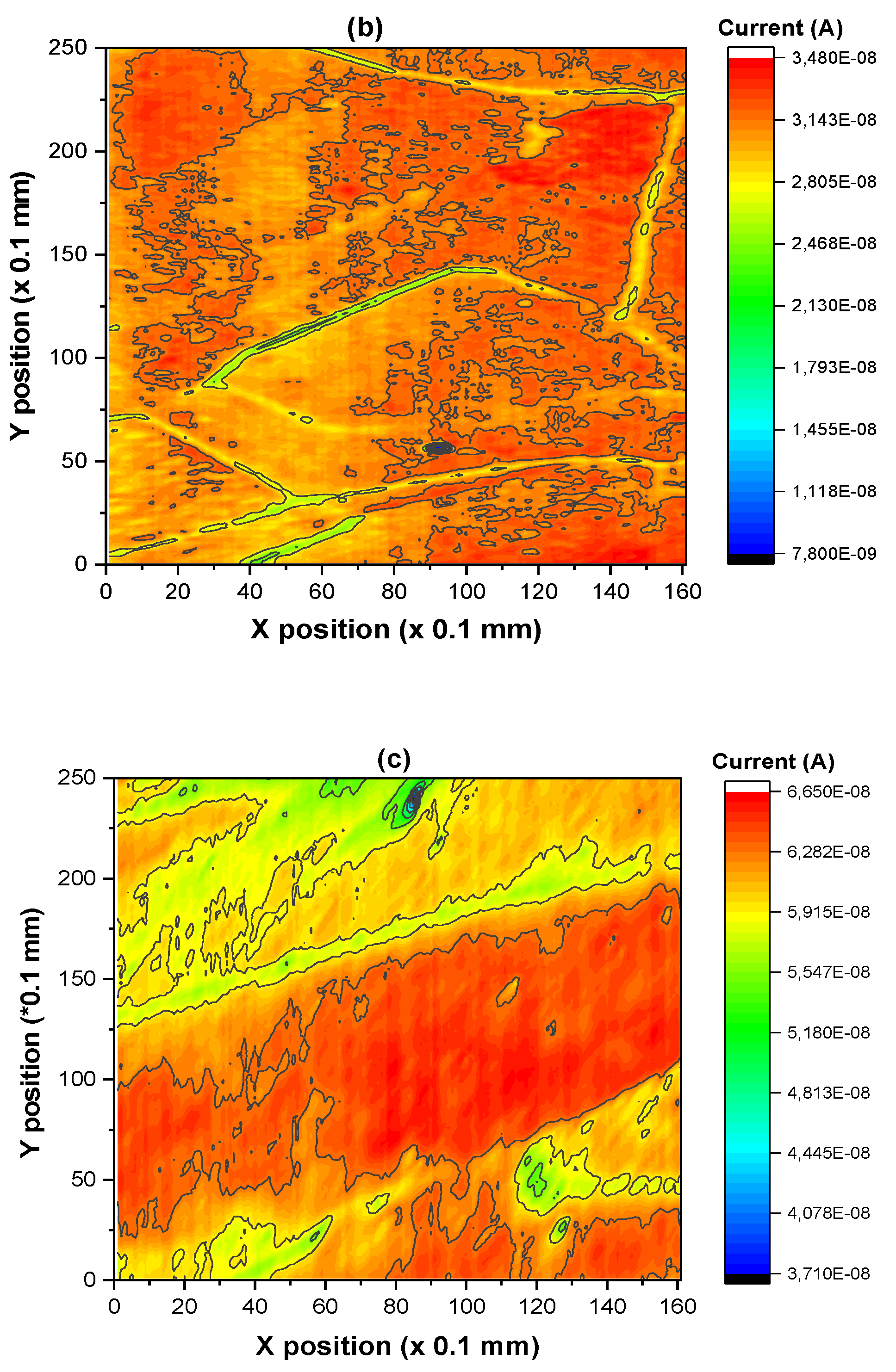
Figure 7 shows the two-dimensional produced current (TDPC) distribution of two samples—the first, Al-NP-coated mc-Si treated with PS, and the second, mc-Si-treated PS-covered SiNx—measured using LBIC performance [32]. It functions by scanning a focused laser beam (638 nm) across mc-Si while measuring the local short-circuit current (Isc, local) generated at each point. This technique produces a spatially resolved map that highlights defects and variations in carrier collection efficiency, which are critical for evaluating the electronic quality of mc-Si. By comparing LBIC measurements before and after treatment, we can assess the impact of treatment processes on mc-Si surface passivation. The laser beam progressively scanned across a region 1.6 × 2.5 cm2, and the TDPC was measured [33]. A significant variation in the TDPC was observed, which can be attributed to variations in defect density. For mc-Si with Al-NP-treated PS, the TDPC showed an improvement compared to bare mc-Si, where the current varied between 1 and 2.8 nA (Figure 7a). However, for mc-Si with Al-NPs treated with porous silicon (Figure 7b), the minimum TDPC value increased to 7.8 nA, with the maximum reaching 34 nA. This improvement in TDPC was attributed to the enhancement of the minority carrier diffusion length and the passivation of recombination centers at both the grains and grain boundaries (GBs), facilitated by Si-Ox and Al-O-Si species, which passivate defects and dangling bonds on the silicon surface [33,34]. For the second sample, mc-Si with PS-covered SiNx (Figure 7c), the minimum GC value increased to 37 nA, and the maximum reached 66 nA due to the well-known role of SiH and SiN bonds in passivating and improving silicon quality [30,31,35]. Overall, the samples obtained offered significant advantages in optical and optoelectronic performance compared to ref mc-Si (Table 1).
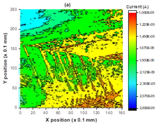
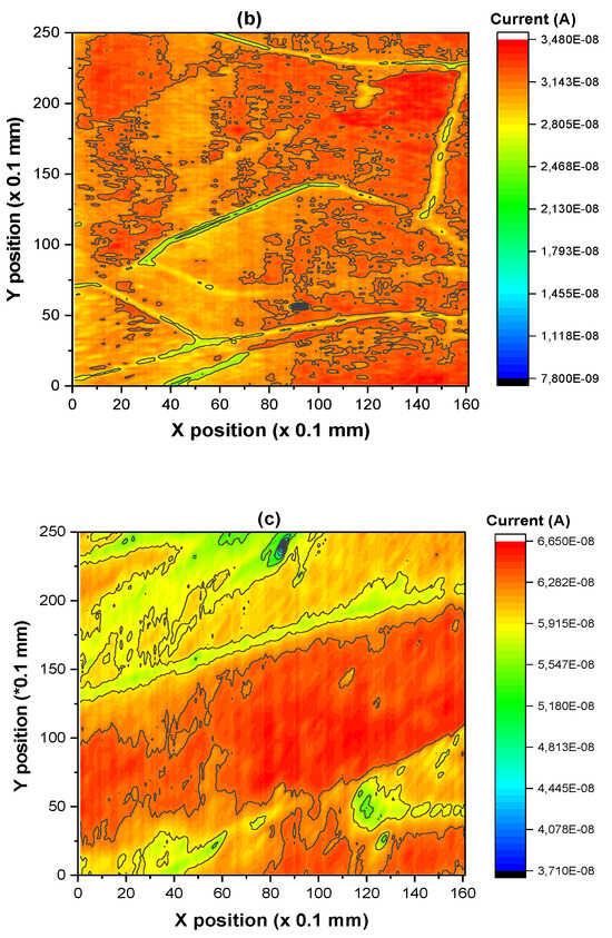
Figure 7.
Two-dimensional produced currents of (a) bare mc-Si (b) mc-Si treated with PS-covered SiNx layer and (c) Al-NP-coated mc-Si treated with PS.

Table 1.
Optical and optoelectronic performance of Al-NP-coated mc-Si treated with PS and mc-Si with PS-covered SiNx samples.
4. Conclusions
The integration of silicon nitride and alumina nanoparticles demonstrates a promising approach to enhancing the electronic quality of mc-Si for solar cell applications. The combined effects of surface passivation, defect reduction, and improved generated current contribute to enhanced solar cell efficiency. We have demonstrated that the substrates of mc-Si with PS-combined SiNx and alumina nanoparticle-covered mc-Si-treated PS exhibit several optical and optoelectronic performance advantages. This approach led to a dramatic decrease in optical reflectivity at 930 nm to 2% for Al-NP-coated mc-Si treated with PS and to 5% for PS-combined SiNx, as well as an enhancement of the diffusion length from 2 µm to 100 µm for Al-NP-coated mc-Si treated with PS and to 300 µm for PS-combined SiNx. However, the generated current improved from 1–2.8 nA for bare mc-Si to 7.8–34 nA for Al-NP-coated mc-Si treated with porous silicon and to 37–66 nA for PS-combined SiNx. The experimental results suggest that the mc-Si with PS-combined SiNx and Al-NP-coated mc-Si treated with porous silicon substrates induce spectacular passivation and higher electronic quality of the mc-Si surface.
Author Contributions
All authors contributed to the study’s conception and design. Conceptualization, M.B.R. and A.E.H.; methodology, A.M.; software, K.C.; validation, M.A.A., W.D. and M.B.R.; formal analysis, A.E.H.; investigation, A.M.; resources, K.C.; data curation, M.A.A.; writing—original draft preparation, W.D.; writing—review and editing, M.B.R.; visualization, K.C.; supervision, M.B.R.; project administration, K.C.; funding acquisition, K.C. All authors have read and agreed to the published version of the manuscript.
Funding
This work was supported and funded by the Deanship of Scientific Research at Imam Mohammad Ibn Saud Islamic University (IMSIU) (grant number IMSIU-DDRSP2502).
Data Availability Statement
The datasets generated and/or analyzed during the current study are available from the corresponding author upon reasonable request.
Conflicts of Interest
The authors declare no conflicts of interest.
Correction Statement
This article has been republished with a minor correction to the existing affiliation information. This change does not affect the scientific content of the article.
References
- Burtescu, S.; Parvulescu, C.; Babarada, F.; Manea, E. The low cost multicrystalline silicon solar cells. Mater. Sci. Eng. B 2009, 165, 190–193. [Google Scholar] [CrossRef]
- Lan, C.W.; Hsu, C.; Nakajima, K. Multicrystalline silicon crystal growth for photovoltaic applications. In Handbook of Crystal Growth; Elsevier: Amsterdam, The Netherlands, 2015; pp. 373–411. [Google Scholar]
- Yu, W.; Xue, Y.; Mei, J.; Zhou, X.; Xiong, M.; Zhang, S. Segregation and removal of transition metal impurities during the directional solidification refining of silicon with Al-Si solvent. J. Alloys Compd. 2019, 805, 198–204. [Google Scholar] [CrossRef]
- Lv, X.; Li, H.; Ding, D.; Yu, X.; Jin, C.; Yang, D. Interfacial characterization of non-metal precipitates at grain boundaries in cast multicrystalline silicon crystals. J. Cryst. Growth 2025, 652, 128042. [Google Scholar] [CrossRef]
- Wang, L.; Liu, J.; Li, Y.; Wei, G.; Li, Q.; Fan, Z.; He, D. Dislocations in Crystalline Silicon Solar Cells. Adv. Energy Sustain. Res. 2024, 5, 2300240. [Google Scholar] [CrossRef]
- Alrasheedi, N.H. The Effects of Porous Silicon and Silicon Nitride Treatments on the Electronic Qualities of Multicrystalline Silicon for Solar Cell Applications. Silicon 2024, 16, 1765–1773. [Google Scholar] [CrossRef]
- Zhou, R.; Li, W.; Ge, B.; Song, J.; Su, Q.; Xi, M.; Liu, Y. Optimization of the deposited Al2O3 thin film process by RS-ALD and edge passivation applications for half-solar cells. Ceram. Int. 2025, 51, 2840–2845. [Google Scholar] [CrossRef]
- Chen, J.; Chen, B.; Lee, W.; Fukuzawa, M.; Yamada, M.; Sekiguchi, T. Grain boundaries in multicrystalline si. Solid State Phenom. 2010, 156, 19–26. [Google Scholar] [CrossRef]
- Woo, S.; Bertoni, M.; Choi, K.; Nam, S.; Castellanos, S.; Powell, D.M.; Choi, H. An insight into dislocation density reduction in multicrystalline silicon. Sol. Energy Mater. Sol. Cells 2016, 155, 88–100. [Google Scholar] [CrossRef]
- Zhang, Y.; Sun, J.; Li, X.; Zhang, D.; Tao, K.; Jiang, S.; Jia, R. Improved performance on multi-crystalline silicon solar cells by optimizing aluminum back surface field process. Mater. Sci. Semicond. Process. 2021, 132, 105916. [Google Scholar] [CrossRef]
- Ayvazyan, G. Crystalline and Porous Silicon. In Black Silicon: Formation, Properties, and Application; Springer Nature Switzerland: Cham, Switzerland, 2024; pp. 1–49. [Google Scholar]
- Lipinski, M.; Panek, P.; Bełtowska, E.; Czternastek, H. Reduction of surface reflectivity by using double porous silicon layers. Mater. Sci. Eng. B 2003, 101, 297–299. [Google Scholar] [CrossRef]
- Mogoda, A.S.; Farag, A.R. The effects of a few formation parameters on porous silicon production in HF/HNO3 using ag-assisted etching and a comparison with a stain etching method. Silicon 2022, 14, 11405–11415. [Google Scholar] [CrossRef]
- Rabha, M.B.; Hajji, M.; Mohamed, S.B.; Hajjaji, A.; Gaidi, M.; Ezzaouia, H.; Bessais, B. Stain-etched porous silicon nanostructures for multicrystalline silicon-based solar cells. Eur. Phys. J.-Appl. Phys. 2012, 57, 21301. [Google Scholar] [CrossRef]
- Faltakh, H.; Bourguiga, R.; Rabha, M.B.; Bessais, B. Simulation and optimization of the performance of multicrystalline silicon solar cell using porous silicon antireflection coating layer. Superlattices Microstruct. 2014, 72, 283–295. [Google Scholar] [CrossRef]
- Ge, D.; Fang, Z.; Zhao, C.; Shi, J.; Zhang, L. Preparation and anti-reflection performance of porous silicon/gold nanocomposite structures. Eur. Phys. J. D 2023, 77, 108. [Google Scholar] [CrossRef]
- Fzaa, W.T.; Tomaa, G.A.; al Qaisy, H.Q.K.; Mutlak, F.A.H. Characterization of the anti-reflectance laser-assisted etched silicon micro-nano structure for solar cell application. J. Opt. 2024, 1–8. [Google Scholar] [CrossRef]
- Harbeke, G.; Jastrzebski, L. Assessment of the surface quality of SIMOX wafers by UV reflectance. J. Electrochem. Soc. 1990, 137, 696. [Google Scholar] [CrossRef]
- Rabha, M.B.; Salem, M.; El Khakani, M.A.; Bessais, B.; Gaidi, M. Monocrystalline silicon surface passivation by Al2O3/porous silicon combined treatment. Mater. Sci. Eng. B 2013, 178, 695–697. [Google Scholar] [CrossRef]
- Cuevas, A.; Macdonald, D. Measuring and interpreting the lifetime of silicon wafers. Sol. Energy 2004, 76, 255–262. [Google Scholar] [CrossRef]
- Khezami, L.; Jemai, A.B.; Alhathlool, R.; Rabha, M.B. Electronic quality improvement of crystalline silicon by stain etching-based PS nanostructures for solar cells application. Sol. Energy 2016, 129, 38–44. [Google Scholar] [CrossRef]
- Porre, O.; Martinuzzi, S.; Pasquinelli, M.; Perichaud, I.; Gay, N. Gettering effect of aluminium in mc-Si and c-Si wafers and in solar cells. In Proceedings of the Conference Record of the Twenty Fifth IEEE Photovoltaic Specialists Conference, Washington, DC, USA, 13–17 May 1996. [Google Scholar]
- Harraz, F.A.; Sakka, T.; Ogata, Y.H. Immersion plating of nickel onto a porous silicon layer from fluoride solutions. Phys. Status Solidi (A) 2003, 197, 51–56. [Google Scholar] [CrossRef]
- Rahmani, M.; Moadhen, A.; Zaibi, M.A.; Elhouichet, H.; Oueslati, M. Photoluminescence enhancement and stabilisation of porous silicon passivated by iron. J. Lumin. 2008, 128, 1763–1766. [Google Scholar] [CrossRef]
- Arnoldbik, W.M.; Habraken, F.H.P.M. Swift heavy ion induced modifications of silicon (sub) oxide nitride layer structures. Nucl. Instrum. Methods Phys. Res. Sect. B Beam Interact. Mater. At. 2007, 256, 300–304. [Google Scholar] [CrossRef]
- Kanemitsu, Y.; Okamoto, S. Resonantly excited photoluminescence from porous silicon: Effects of surface oxidation on resonant luminescence spectra. Phys. Rev. B 1997, 56, R1696. [Google Scholar] [CrossRef]
- Maruyama, T.; Ohtani, S. Photoluminescence of porous silicon exposed to ambient air. Appl. Phys. Lett. 1994, 65, 1346–1348. [Google Scholar] [CrossRef]
- Kanemitsu, Y.; Futagi, T.; Matsumoto, T.; Mimura, H. Origin of the blue and red photoluminescence from oxidized porous silicon. Phys. Rev. B 1994, 49, 14732. [Google Scholar] [CrossRef]
- Stannowski, B.; Rath, J.K.; Schropp, R.E.I. Growth process and properties of silicon nitride deposited by hot-wire chemical vapor deposition. J. Appl. Phys. 2003, 93, 2618–2625. [Google Scholar] [CrossRef]
- Lelièvre, J.F.; Fourmond, E.; Kaminski, A.; Palais, O.; Ballutaud, D.; Lemiti, M. Study of the composition of hydrogenated silicon nitride SiNx: H for efficient surface and bulk passivation of silicon. Sol. Energy Mater. Sol. Cells 2009, 93, 1281–1289. [Google Scholar] [CrossRef]
- Dao, V.A.; Heo, J.; Kim, Y.; Kim, K.; Lakshminarayan, N.; Yi, J. Optimized surface passivation of n and p type silicon wafers using hydrogenated SiNx layers. J. Non-Cryst. Solids 2010, 356, 2880–2883. [Google Scholar] [CrossRef]
- Dimassi, W.; Derbali, L.; Bouaıcha, M.; Bessaıs, B.; Ezzaouia, H. Two-dimensional LBIC and Internal-Quantum-Efficiency investigations of grooved grain boundaries in multicrystalline silicon solar cells. Sol. Energy 2011, 85, 350–355. [Google Scholar] [CrossRef]
- Ben Rabha, M.; Dimassi, W.; Bouaicha, M.; Ezzaouia, H.; Bessais, B. Laser-beam-induced current mapping evaluation of porous silicon-based passivation in polycrystalline silicon solar cells. Sol. Energy 2009, 83, 721. [Google Scholar] [CrossRef]
- Achref, M.; Khezami, L.; Mokraoui, S.; Rabha, M.B. Effective surface passivation on multi-crystalline silicon using aluminum/porous silicon nanostructures. Surf. Interfaces 2020, 18, 100391. [Google Scholar] [CrossRef]
- Krotkus, A.; Grigoras, K.; Pacebutas, V.; Barsony, I.; Vazsonyi, E.; Fried, M.; Szlafcik, J.; Nijs, J.; Levy-Clement, C. Efficiency improvement by porous silicon coating of multicrystalline solar cells. Sol. Energy Mater. Sol. Cells 1997, 45, 267. [Google Scholar] [CrossRef]

Disclaimer/Publisher’s Note: The statements, opinions and data contained in all publications are solely those of the individual author(s) and contributor(s) and not of MDPI and/or the editor(s). MDPI and/or the editor(s) disclaim responsibility for any injury to people or property resulting from any ideas, methods, instructions or products referred to in the content. |
© 2025 by the authors. Licensee MDPI, Basel, Switzerland. This article is an open access article distributed under the terms and conditions of the Creative Commons Attribution (CC BY) license (https://creativecommons.org/licenses/by/4.0/).