Growth of Catalyst-Free Hexagonal Pyramid-Like InN Nanocolumns on Nitrided Si(111) Substrates via Radio-Frequency Metal–Organic Molecular Beam Epitaxy

 ,
, 


Abstract
1. Introduction
2. Materials and Methods
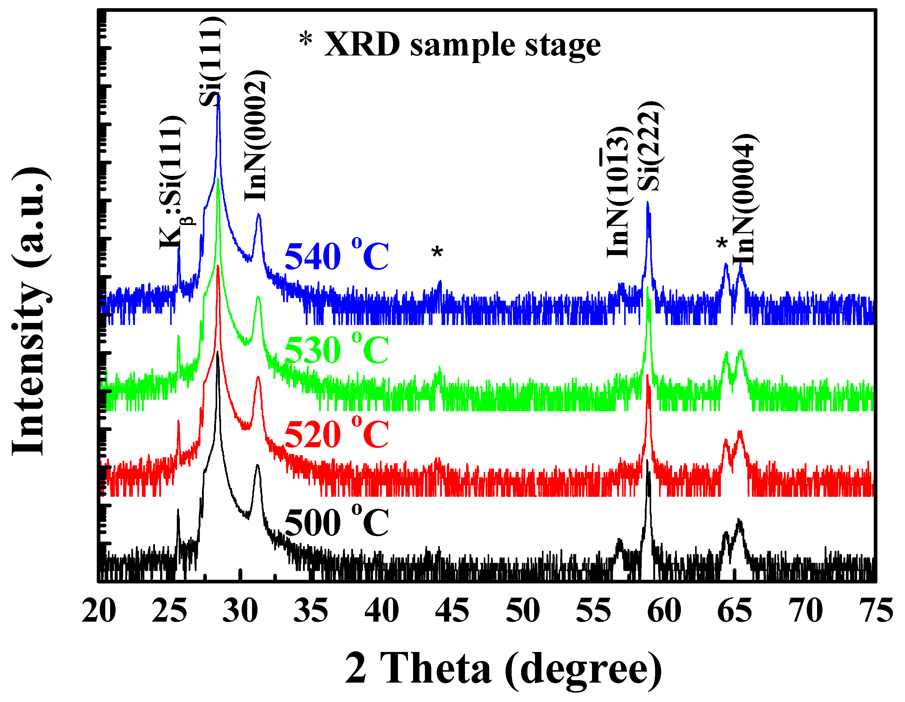
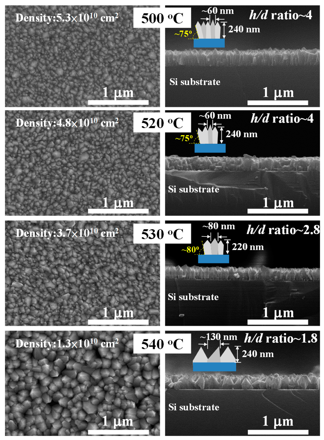
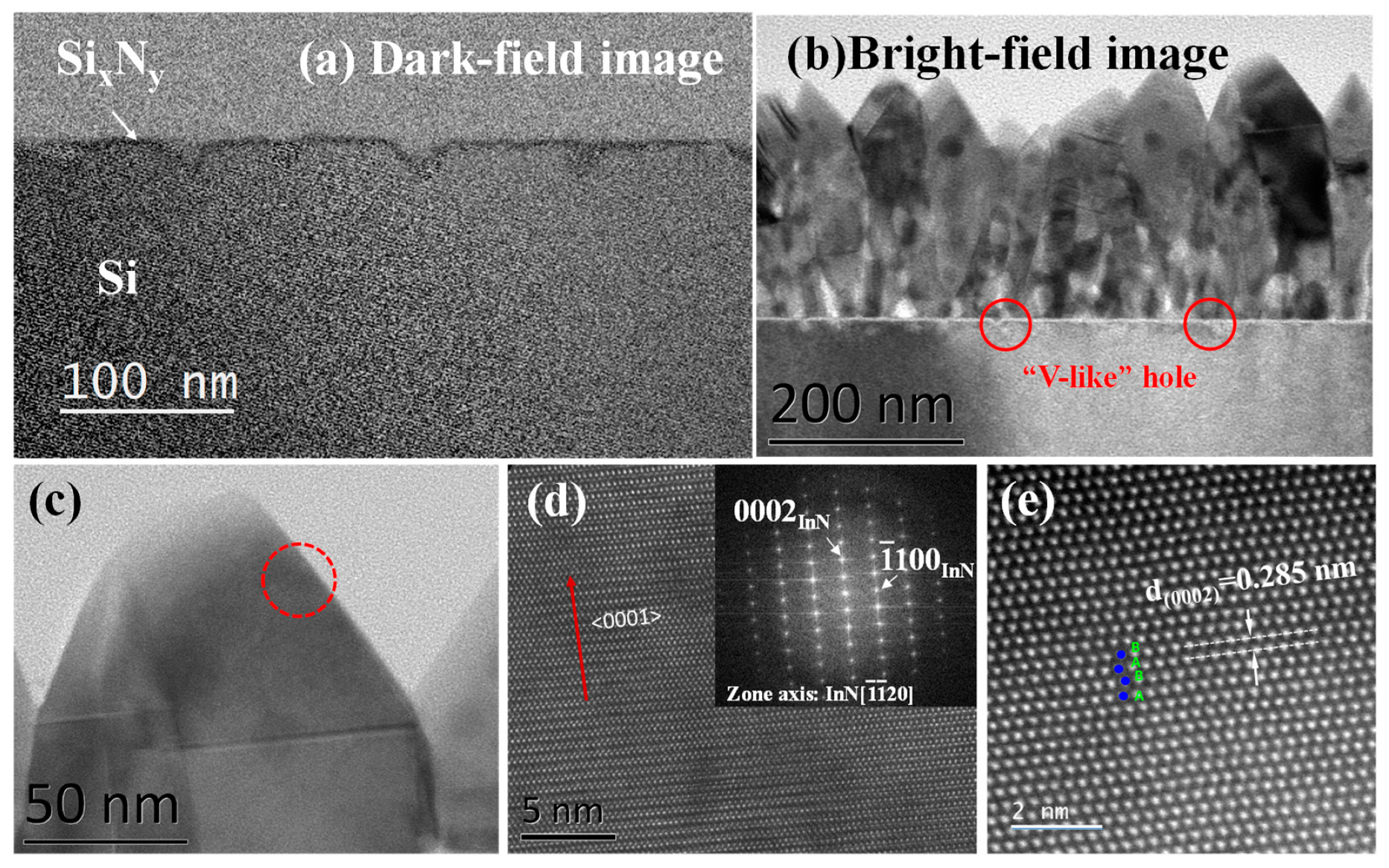
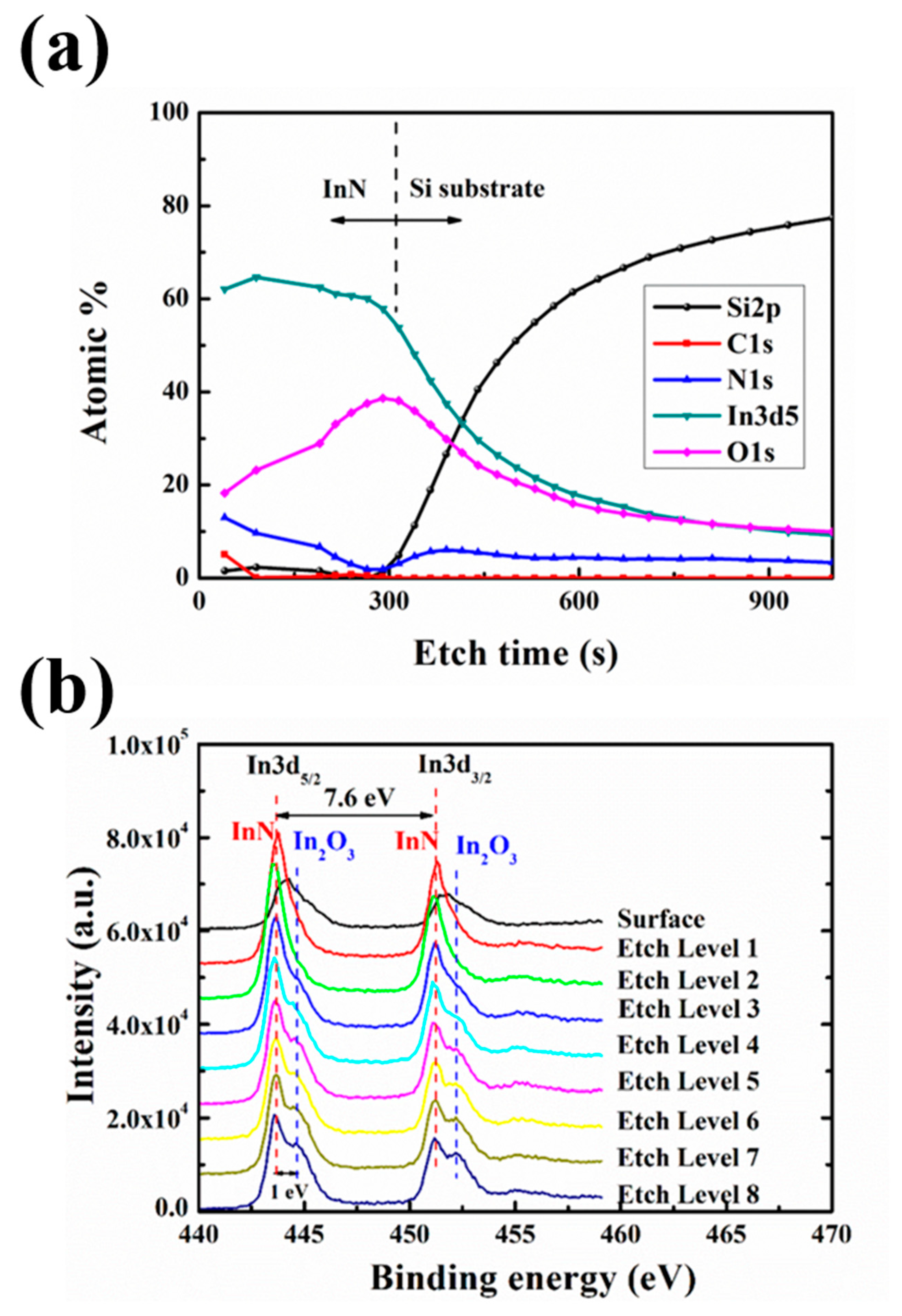
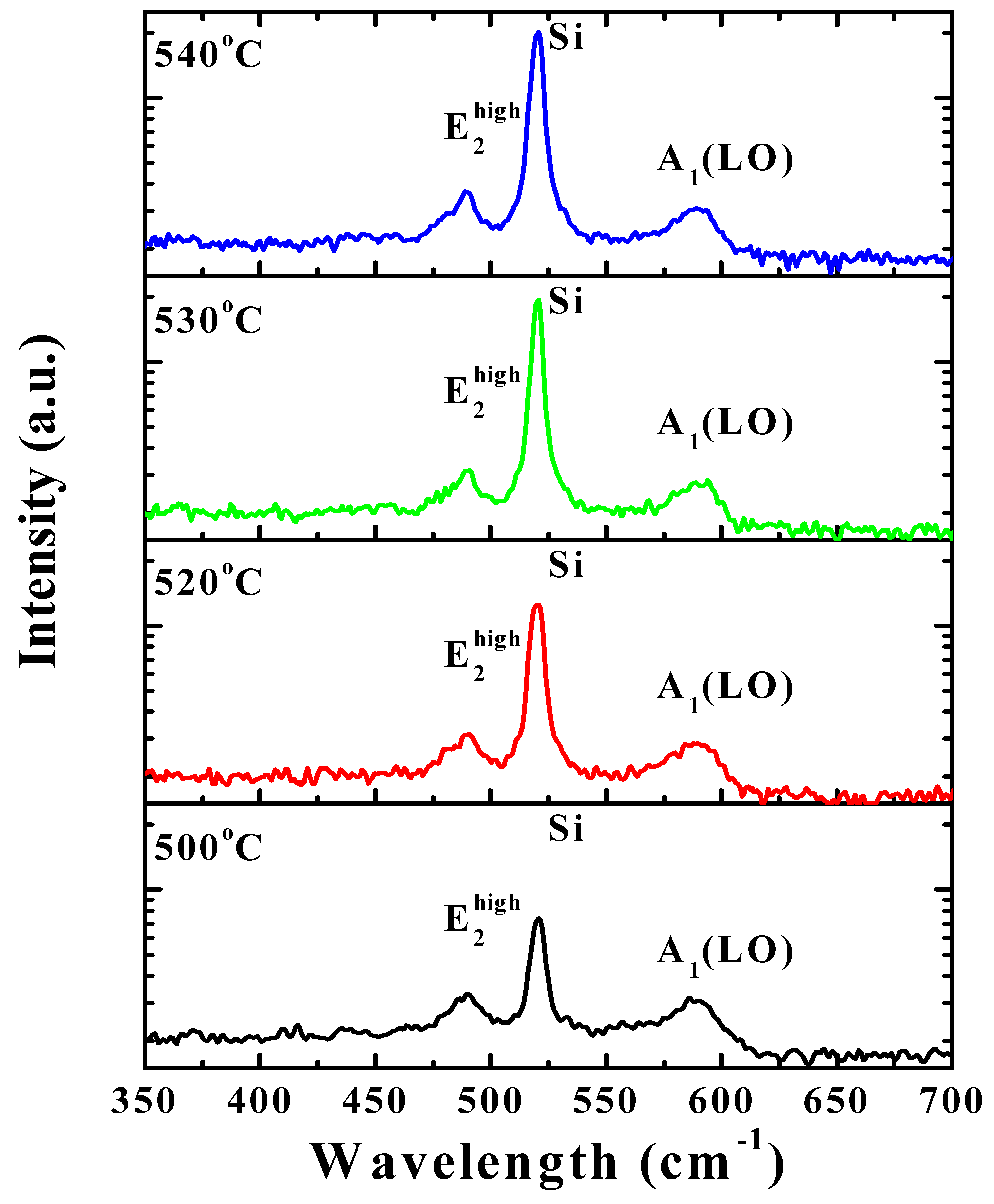
3. Results and Discussion
4. Conclusions
Author Contributions
Funding
Acknowledgments
Conflicts of Interest
References
- Bhuiyan, A.G.; Hashimoto, A.; Yamamoto, A. Indium nitride (InN): A review on growth, characterization, and properties. J. Appl. Phys. 2003, 94, 2779–2808. [Google Scholar] [CrossRef]
- Wu, J. When group-III nitrides go infrared: New properties and perspectives. J. Appl. Phys. 2009, 106, 011101. [Google Scholar] [CrossRef]
- Wu, J.; Walukiewicz, W.; Yu, K.M.; Ager, J.W.; Haller, E.E.; Lu, H.; Schaff, W.J.; Saito, Y.; Nanishi, Y. Unusual properties of the fundamental band gap of InN. Appl. Phys. Lett. 2002, 80, 3967–3969. [Google Scholar] [CrossRef]
- Feneberg, M.; Däubler, J.; Thonke, K.; Sauer, R.; Schley, P.; Goldhahn, R. Mahan excitons in degenerate wurtzite InN: Photoluminescence spectroscopy and reflectivity measurements. Phys. Rev. B 2008, 77, 245207. [Google Scholar] [CrossRef]
- Higashiwaki, M.; Matsui, T. Epitaxial growth of high-quality InN films on sapphire substrates by plasma-assisted molecular-beam epitaxy. J. Cryst. Growth 2003, 252, 128–135. [Google Scholar] [CrossRef]
- Feng, S.; Tan, J.; Li, B.; Song, H.; Wu, Z.; Chen, X. Nitridation effects of Si(111) substrate surface on InN nanorods grown by plasma-assisted molecular beam epitaxy. J. Alloys Compd. 2015, 621, 232–237. [Google Scholar] [CrossRef]
- Yamamoto, A.; Yamauchi, Y.; Ohkubo, M.; Hashimoto, A.; Saitoh, T. Heteroepitaxial growth of InN on Si(111) using a GaAs intermediate layer. Solid State Electron. 1997, 41, 149–154. [Google Scholar] [CrossRef]
- Ahn, H.; Shen, C.H.; Wu, C.L.; Gwo, S. Spectroscopic ellipsometry study of wurtzite InN epitaxial films on Si (111) with varied carrier concentrations. Appl. Phys. Lett. 2005, 86, 201905. [Google Scholar] [CrossRef]
- Kumar, M.; Rajpalke, M.K.; Bhat, T.N.; Roul, B.; Sinha, N.; Kalghatgi, A.T.; Krupanidhi, S.B. Growth of InN layers on Si (111) using ultra thin silicon nitride buffer layer by NPA-MBE. Mater. Lett. 2011, 65, 1396–1399. [Google Scholar] [CrossRef]
- Pan, Y.; Wang, T.; Shen, K.; Peng, T.; Wu, K.; Zhang, W.; Liu, C. Rapid growth and characterization of InN nanocolumns on InGaN buffer layers at a low ratio of N/In. J. Cryst. Growth 2010, 313, 16–19. [Google Scholar] [CrossRef]
- Gauckler, L.J.; Lukas, H.L.; Tien, T.Y. Crystal chemistry of β-Si3N4 solid solutions containing metal oxides. Mater. Res. Bull. 1976, 11, 503–512. [Google Scholar] [CrossRef][Green Version]
- Grandal, J.; Sánchez-García, M.A.; Calleja, E.; Gallardo, E.; Calleja, J.M.; Luna, E.; Trampert, A.; Jahn, A. InN nanocolumns grown by plasma-assisted molecular beam epitaxy on A-plane GaN templates. Appl. Phys. Lett. 2009, 95, 029901. [Google Scholar] [CrossRef]
- Monteagudo-Lerma, L.; Valdueza-Felip, S.; Núñez-Cascajero, A.; Ruiz, A.; González-Herráez, M.; Monroy, E.; Naranjo, F.B. Morphology and arrangement of InN nanocolumns deposited by radio-frequency sputtering: Effect of the buffer layer. J. Cryst. Growth 2016, 434, 13–18. [Google Scholar] [CrossRef]
- Yun, S.H.; Ra, Y.H.; Lee, Y.M.; Song, K.Y.; Cha, J.H.; Lim, H.C.; Kim, D.W.; Suthan Kissinger, N.J.; Lee, C.R. Growth of hexagonal and cubic InN nanowires using MOCVD with different growth temperatures. J. Cryst. Growth 2010, 312, 2201–2205. [Google Scholar] [CrossRef]
- Kuo, S.Y.; Lai, F.-I.; Chen, W.C.; Hsiao, C.N. Catalyst-free growth and characterization of gallium nitride nanorods. J. Cryst. Growth 2008, 310, 5129–5133. [Google Scholar] [CrossRef]
- Chen, W.C.; Kuo, S.Y.; Lai, F.-I.; Lin, W.T.; Hsiao, C.N. Effect of substrate temperature on structural and optical properties of InN epilayer grown on GaN template. Thin Solid Films 2013, 529, 169–172. [Google Scholar] [CrossRef]
- Segura-Ruiz, J.; Garro, N.; Cantarero, A.; Denker, C.; Malindretos, J.; Rizzi, A. Optical studies of MBE-grown InN nanocolumns: Evidence of surface electron accumulation. Phys. Rev. B 2009, 79, 115305. [Google Scholar] [CrossRef]
- Park, S.E.; Lim, S.M.; Lee, C.R.; Kim, C.S.; Byungsung, O. Influence of SiN buffer layer in GaN epilayers. J. Cryst. Growth 2003, 249, 487–491. [Google Scholar] [CrossRef]
- Nishikawa, S.; Nakao, Y.; Naoi, H.; Araki, T.; Nab, H.; Nanishi, Y. Growth of InN nanocolumns by RF-MBE. J. Cryst. Growth 2007, 301–302, 490–495. [Google Scholar] [CrossRef]
- Grandal, J.; Sánchez-García, M.A.; Calleja, E. Accommodation mechanism of InN nanocolumns grown on Si (111) substrates by molecular beam epitaxy. Appl. Phys. Lett. 2007, 91, 021902. [Google Scholar] [CrossRef]
- Lee, S.H.; Jang, E.S.; Kim, D.W.; Lee, I.H.; Navamathavan, R.; Kannappan, S.; Lee, C.R. InN nanocolumns grown on a Si(111) substrate using Au+In solid solution by metal organic chemical vapor deposition. Jpn. J. Appl. Phys. 2009, 48, 04C141-1–04C141-3. [Google Scholar] [CrossRef]
- Tansley, T.L.; Foley, C.P. Optical band gap of indium nitride. J. Appl. Phys. 1986, 59, 3241–3244. [Google Scholar] [CrossRef]
- Stoica, T.; Meijers, R.; Calarco, R.; Richter, T.; Lüth, H. MBE growth optimization of InN nanowires. J. Cryst. Growth 2006, 290, 241–247. [Google Scholar] [CrossRef]
- Denker, C.; Malindretos, J.; Werner, F.; Limbach, F.; Schuhmann, H.; Niermann, T.; Seibt, M.; Rizzi, A. Self-organized growth of InN-nanocolumns on p-Si(111) by MBE. Phys. Status Solidi C 2008, 5, 1706–1708. [Google Scholar] [CrossRef]
- Wu, C.-L.; Chen, W.-S.; Su, Y. N2-plasma nitridation on Si(111): Its effect on crystalline silicon nitride growth. Surf. Sci. 2012, 606, L51–L54. [Google Scholar] [CrossRef]
- Yamamoto, A.; Tsujino, M.; Ohkubo, M.; Hashimoto, A. Nitridation effects of substrate surface on the metalorgantic chemical vapor deposition growth of InN on Si and a-Al2O3 substrates. J. Cryst. Growth 1994, 137, 415–420. [Google Scholar] [CrossRef]
- Chen, W.-C.; Chen, H.-P.; Kuo, S.-Y.; Lai, F.I.; Hsiao, C.-N.; Lee, C.-C. Evaluation of the impact of Tmin flow rate on the structural and optical properties of InN/ZnO heterojunctions using RF-MOMBE. J. Cryst. Growth 2017, 475, 88–92. [Google Scholar] [CrossRef]
- Specht, P.; Armitage, R.; Ho, J.; Gunawan, E.; Yang, Q.; Xu, X.; Kisielowski, C.; Weber, E.R. The influence of structural properties on conductivity and luminescence of MBE grown InN. J. Cryst. Growth 2004, 269, 111–118. [Google Scholar] [CrossRef]
- Iwao, K.; Yamamoto, A.; Hashimoto, A. Origins of n-type residual carriers in RF-MOMBE grown InN layers. Phys. Status Solidi C 2007, 4, 2453–2456. [Google Scholar] [CrossRef]
- Chen, W.-C.; Tian, J.-S.; Wu, Y.H.; Wang, W.L.; Kuo, S.-Y.; Lai, F.I.; Chang, L. Influence of V/III Flow Ratio on Growth of InN on GaN by PA-MOMBE. ECS J. Solid State Sci. Technol. 2013, 2, P305–P310. [Google Scholar] [CrossRef]
- Moulder, J.F.; Stickle, W.F.; Sobol, P.E.; Bomben, K.D. Handbook of X-Ray Photoelectron Spectroscopy: A Reference Book of Standard Spectra for Identification and Interpretation of XPS Data; Chastain, J., Ed.; Perkin-Elmer Corporation, Physical Electronics Division: Eden Prairie, MN, USA, 1992. [Google Scholar]
- Parala, H.; Devi, A.; Hipler, F.; Maile, E.; Birkner, A.; Becker, H.W.; Fischer, R.A. Investigations on InN whiskers grown by chemical vapour deposition. J. Cryst. Growth 2001, 231, 68–74. [Google Scholar] [CrossRef]
- Masuda, Y.; Kondo, M.; Koumoto, K. Site-selective deposition of In2O3 using a self-assembled monolayer. Cryst. Growth Des. 2009, 9, 555–561. [Google Scholar] [CrossRef]
- Pu, X.D.; Chen, J.; Shen, W.Z.; Ogawa, H.; Guo, Q.X. Temperature dependence of Raman scattering in hexagonal indium nitride films. J. Appl. Phys. 2005, 98, 033527. [Google Scholar] [CrossRef]
- Briot, O.; Maleyre, B.; Ruffenach, S.; Gil, B.; Pinquier, C.; Demangeot, F.; Frandon, J. Absorption and Raman scattering processes in InN films and dots. J. Cryst. Growth 2004, 269, 22–28. [Google Scholar] [CrossRef]
- Qian, Z.G.; Shen, W.Z.; Ogawa, H.; Guo, Q.X. Experimental studies of lattice dynamical properties in indium nitride. J. Phys. Condens. Matter 2004, 16, R381–R414. [Google Scholar] [CrossRef]


© 2019 by the authors. Licensee MDPI, Basel, Switzerland. This article is an open access article distributed under the terms and conditions of the Creative Commons Attribution (CC BY) license (http://creativecommons.org/licenses/by/4.0/).
Share and Cite
Chen, W.-C.; Yu, T.-Y.; Lai, F.-I.; Chen, H.-P.; Lin, Y.-W.; Kuo, S.-Y. Growth of Catalyst-Free Hexagonal Pyramid-Like InN Nanocolumns on Nitrided Si(111) Substrates via Radio-Frequency Metal–Organic Molecular Beam Epitaxy. Crystals 2019, 9, 291. https://doi.org/10.3390/cryst9060291
Chen W-C, Yu T-Y, Lai F-I, Chen H-P, Lin Y-W, Kuo S-Y. Growth of Catalyst-Free Hexagonal Pyramid-Like InN Nanocolumns on Nitrided Si(111) Substrates via Radio-Frequency Metal–Organic Molecular Beam Epitaxy. Crystals. 2019; 9(6):291. https://doi.org/10.3390/cryst9060291
Chicago/Turabian StyleChen, Wei-Chun, Tung-Yuan Yu, Fang-I Lai, Hung-Pin Chen, Yu-Wei Lin, and Shou-Yi Kuo. 2019. "Growth of Catalyst-Free Hexagonal Pyramid-Like InN Nanocolumns on Nitrided Si(111) Substrates via Radio-Frequency Metal–Organic Molecular Beam Epitaxy" Crystals 9, no. 6: 291. https://doi.org/10.3390/cryst9060291
APA StyleChen, W.-C., Yu, T.-Y., Lai, F.-I., Chen, H.-P., Lin, Y.-W., & Kuo, S.-Y. (2019). Growth of Catalyst-Free Hexagonal Pyramid-Like InN Nanocolumns on Nitrided Si(111) Substrates via Radio-Frequency Metal–Organic Molecular Beam Epitaxy. Crystals, 9(6), 291. https://doi.org/10.3390/cryst9060291