
Graphene-Assisted Polymer Waveguide Optically Controlled Switch Using First-Order Mode


Abstract
:
1. Introduction
2. Materials and Methods
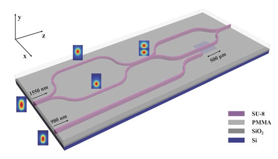
2.1. Materials
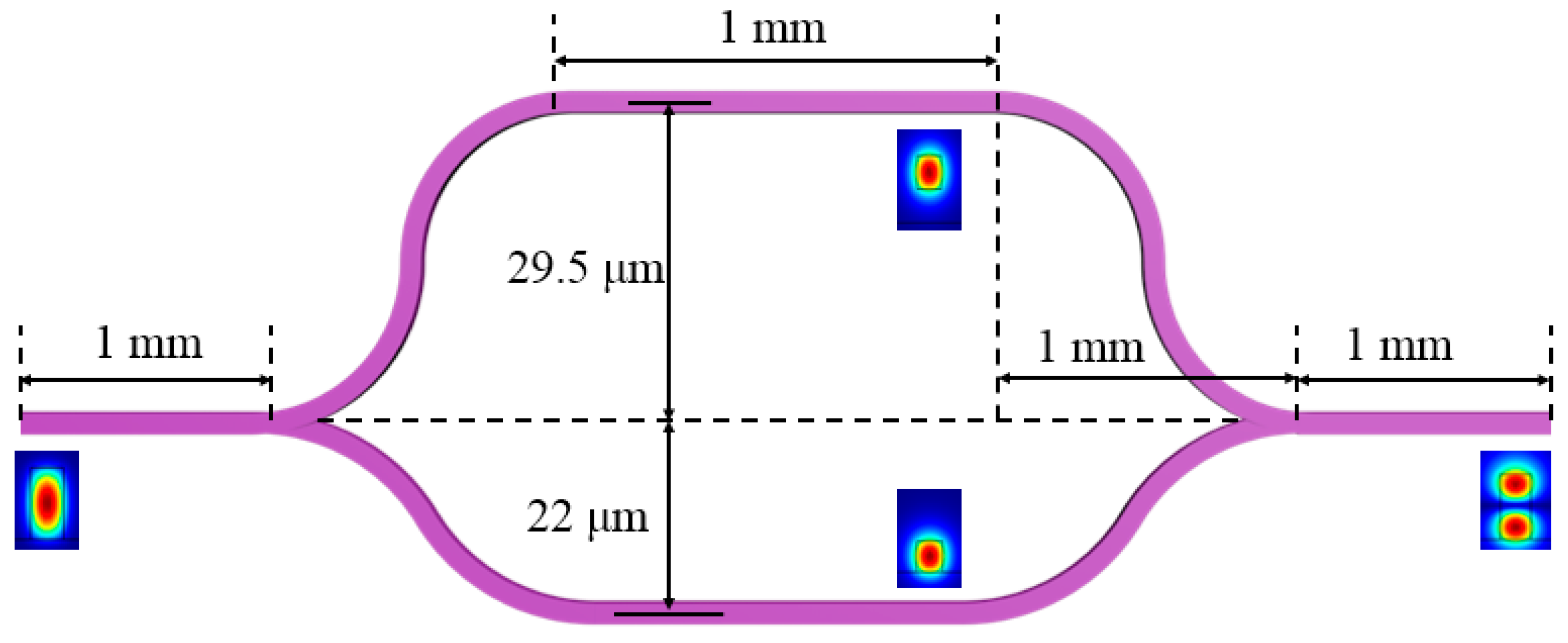
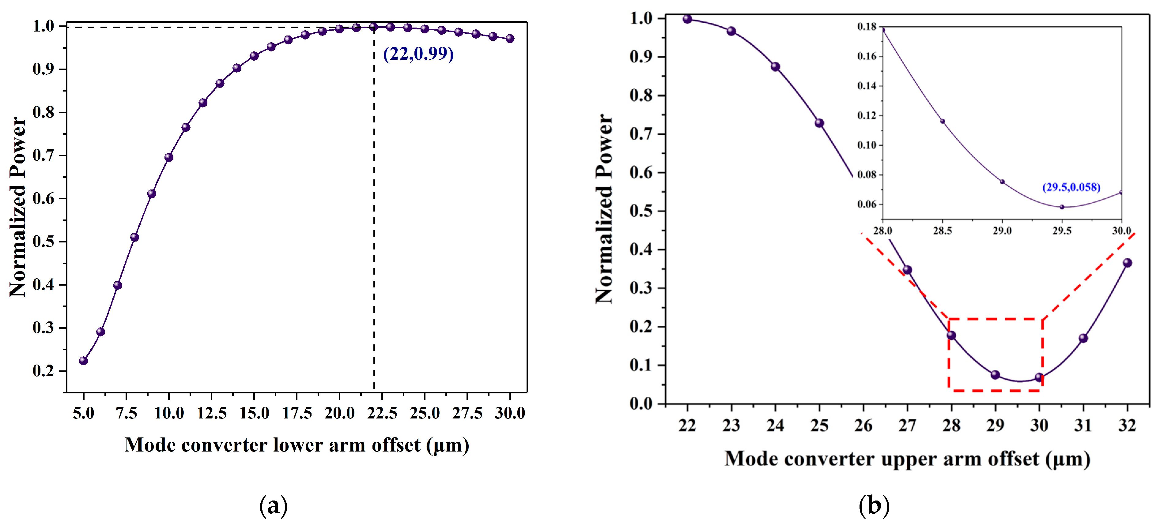
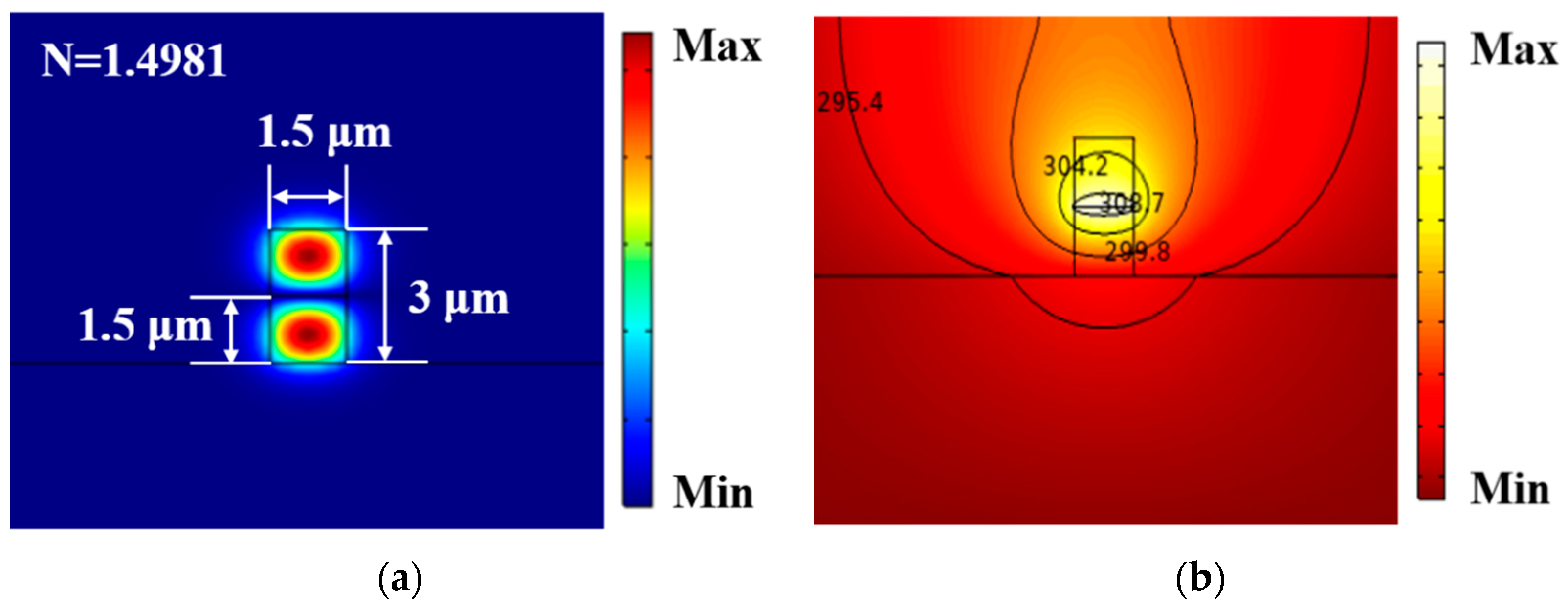
2.2. Mode Converter
2.3. Coupler
2.4. Method
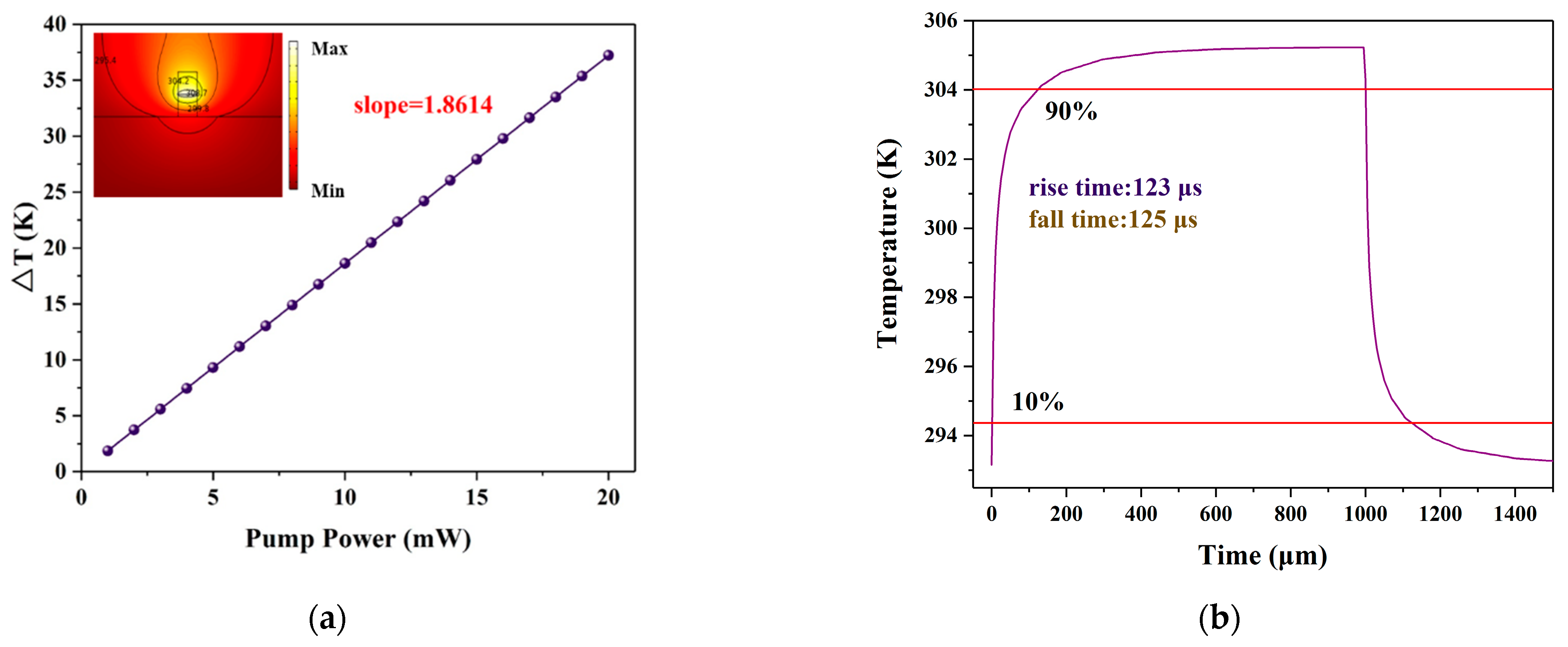
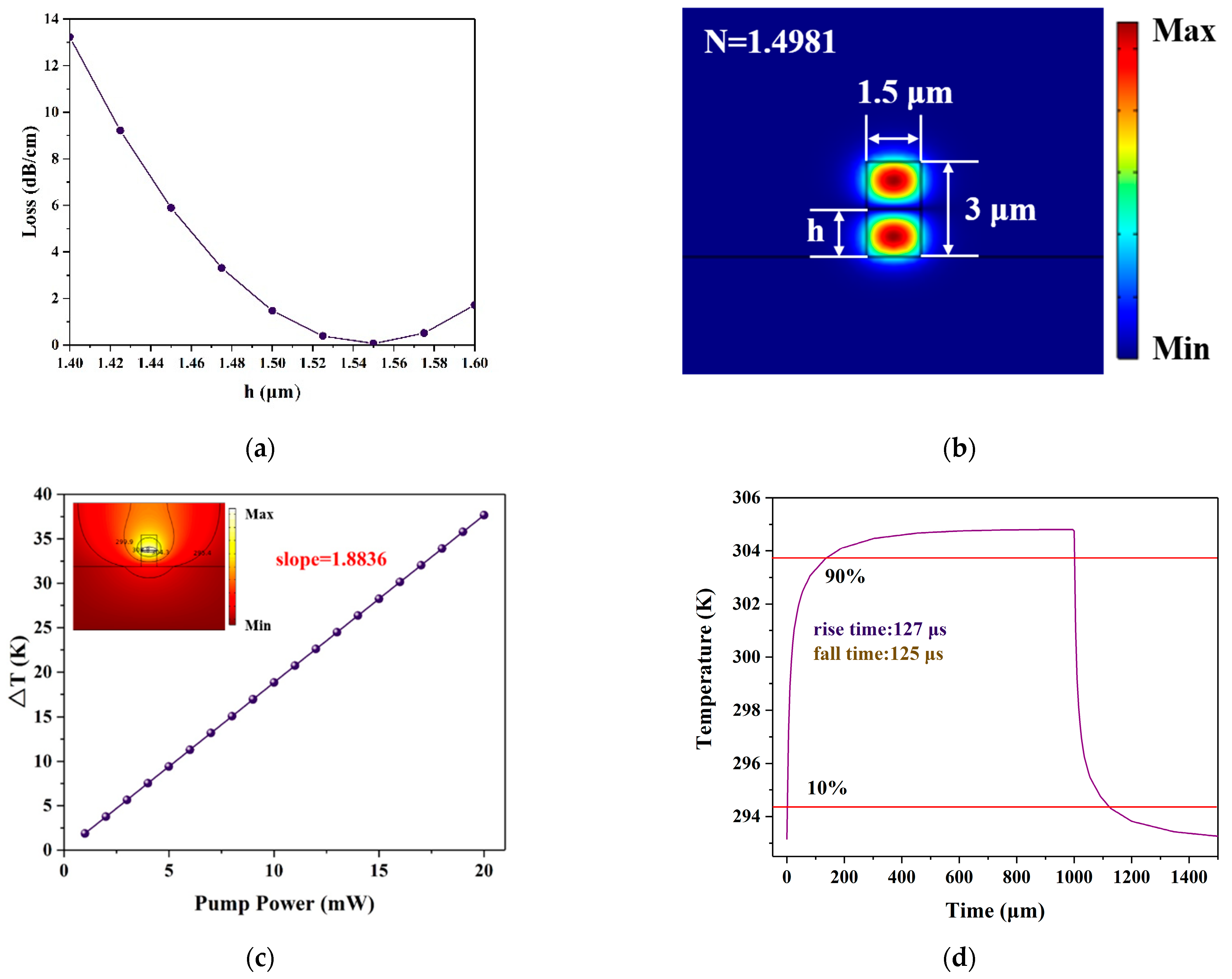
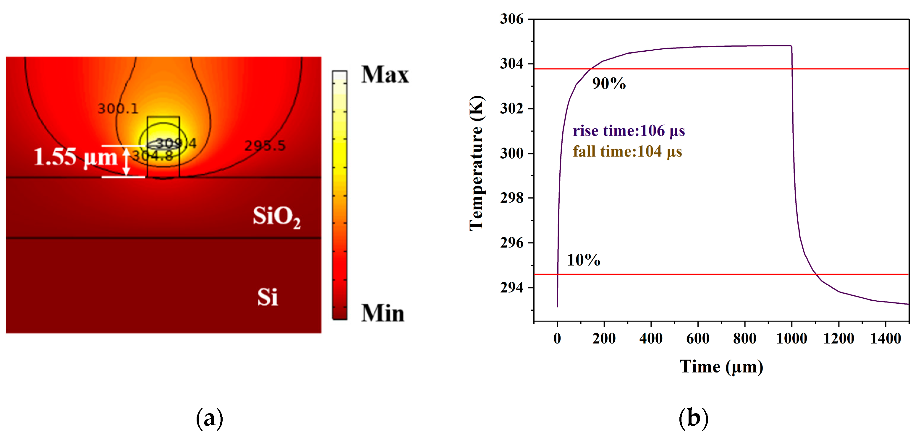
3. Results and Discussion
4. Conclusions
Author Contributions
Funding
Conflicts of Interest
References
- Elbialy, S.; Yousif, B.; Samra, A. Modeling and Performance Enhancement of Active Hybrid Plasmonic Electro-optic Routing Switch. Plasmonics 2020, 15, 2095–2107. [Google Scholar] [CrossRef]
- Zhang, X.; Chen, H.; Liu, L.; Shang, J.; Yu, L.; Li, K.; Dong, J.; Qiu, W.; Guan, H.; Lu, H.; et al. An Optical Switch Based on Electro-Optic Mode Deflection in Lithium Niobate Waveguide. IEEE Photonics Technol. Lett. 2020, 32, 1295–1298. [Google Scholar] [CrossRef]
- Sun, Y.; Cao, Y.; Wang, Q.; Yi, Y.; Sun, X.; Wu, Y.; Wang, F.; Zhang, D. Polymer thermal optical switch for a flexible photonic circuit. Appl. Opt. 2018, 57, 14–17. [Google Scholar] [CrossRef] [PubMed]
- Cao, Y.; Yi, Y.J.; Lin, B.Z.; Sun, Y.; Che, X.C.; Zheng, J.; Wang, F.; Zhang, D.M. Polymer/glass hybrid DC-MZI thermal optical switch for 3D-integrated chips. RSC Adv. 2019, 9, 10651–10656. [Google Scholar] [CrossRef] [Green Version]
- Yang, X.; Long, Q.; Liu, Z.; Zhang, Y.; Yang, J.; Kong, D.; Yuan, L.; Oh, K. Microfiber interferometer integrated with Au nanorods for an all-fiber phase shifter and switch. Opt. Lett. 2019, 44, 1092–1095. [Google Scholar] [CrossRef]
- Wu, L.; Jiang, X.; Zhao, J.; Liang, W.; Li, Z.; Huang, W.; Lin, Z.; Wang, Y.; Zhang, F.; Lu, S.; et al. MXene-Based Nonlinear Optical Information Converter for All-Optical Modulator and Switcher. Laser Photonics Rev. 2018, 12, 1800215. [Google Scholar] [CrossRef]
- Wu, K.; Guo, C.; Wang, H.; Zhang, X.; Wang, J.; Chen, J. All-optical phase shifter and switch near 1550nm using tungsten disulfide (WS2) deposited tapered fiber. Opt. Express 2017, 25, 17639–17649. [Google Scholar] [CrossRef]
- Wang, C.; Wang, Y.; Jiang, X.; Xu, J.; Huang, W.; Zhang, F.; Liu, J.; Yang, F.; Song, Y.; Ge, Y.; et al. MXene Ti3C2Tx: A Promising Photothermal Conversion Material and Application in All-Optical Modulation and All-Optical Information Loading. Adv. Opt. Mater. 2019, 7, 1900060. [Google Scholar] [CrossRef]
- Li, W.; Chen, B.G.; Meng, C.; Fang, W.; Xiao, Y.; Li, X.Y.; Hu, Z.F.; Xu, Y.X.; Tong, L.M.; Wang, H.Q.; et al. Ultrafast All-Optical Graphene Modulator. Nano Lett. 2014, 14, 955–959. [Google Scholar] [CrossRef]
- Gao, L.; Ran, H.; Cao, Y.; Li, Y.; Huang, W.; Huang, L.; Feng, D.; Tang, X.; Zhu, T. Coherent optical modulation of graphene based on coherent population oscillation. Opt. Lett. 2019, 44, 223–226. [Google Scholar] [CrossRef]
- Grotevent, M.J.; Hail, C.U.; Yakunin, S.; Dirin, D.N.; Thodkar, K.; Barin, G.B.; Guyot-Sionnest, P.; Calame, M.; Poulikakos, D.; Kovalenko, M.V.; et al. Nanoprinted Quantum Dot-Graphene Photodetectors. Adv. Opt. Mater. 2019, 7, 1900019. [Google Scholar] [CrossRef]
- Cai, K.S.; Li, Y.E.; Wei, W.J.; Mu, X.J.; Ma, A.N.; Wang, Z.; Song, D.M. TM-pass polarizer based on multilayer graphene polymer waveguide. Optoelectron. Lett. 2018, 14, 180–184. [Google Scholar] [CrossRef]
- Zhang, R.L.; Wang, J.; Liao, M.S.; Li, X.; Guan, P.W.; Liu, Y.Y.; Zhou, Y.; Gao, W.Q. Generation of wide-bandwidth pulse with graphene saturable absorber based on tapered fiber. Chin. Phys. B 2019, 28, 180–184. [Google Scholar] [CrossRef]
- Wu, K.; Wang, Y.; Qiu, C.; Chen, J. Thermo-optic all-optical devices based on two-dimensional materials. Photonics Res. 2018, 6, C22–C28. [Google Scholar] [CrossRef]
- Wang, Y.; Gan, X.; Zhao, C.; Fang, L.; Mao, D.; Xu, Y.; Zhang, F.; Xi, T.; Ren, L.; Zhao, J. All-optical control of microfiber resonator by graphene’s photothermal effect. Appl. Phys. Lett. 2016, 108, 171905. [Google Scholar] [CrossRef]
- Gan, X.; Zhao, C.; Wang, Y.; Mao, D.; Fang, L.; Han, L.; Zhao, J. Graphene-assisted all-fiber phase shifter and switching. Optica 2015, 2, 468–471. [Google Scholar] [CrossRef]
- Chu, R.; Guan, C.; Bo, Y.; Liu, J.; Shi, J.; Yang, J.; Ye, P.; Li, P.; Yang, J.; Yuan, L. Graphene decorated twin-core fiber Michelson interferometer for all-optical phase shifter and switch. Opt. Lett. 2020, 45, 177–180. [Google Scholar] [CrossRef]
- Liu, M.; Yin, X.; Ulin-Avila, E.; Geng, B.; Zentgraf, T.; Ju, L.; Wang, F.; Zhang, X. A graphene-based broadband optical modulator. Nature 2011, 474, 64–67. [Google Scholar] [CrossRef]
- Wang, X.; Jin, W.; Chang, Z.; Chiang, K.S. Buried graphene electrode heater for a polymer waveguide thermo-optic device. Opt. Lett. 2019, 44, 1480–1483. [Google Scholar] [CrossRef]
- Chang, Z.; Chiang, K.S. All-optical loss modulation with graphene-buried polymer waveguides. Opt. Lett. 2019, 44, 3685–3688. [Google Scholar] [CrossRef]
- Chang, Z.; Chiang, K.S. Experimental verification of optical models of graphene with multimode slab waveguides. Opt. Lett. 2016, 41, 2129–2132. [Google Scholar] [CrossRef] [PubMed]
- Lv, J.; Yang, Y.; Lin, B.; Cao, Y.; Zhang, Y.; Li, S.; Yi, Y.; Wang, F.; Zhang, D. Graphene-embedded first-order mode polymer Mach-Zender interferometer thermo-optic switch with low power consumption. Opt. Lett. 2019, 44, 4606–4609. [Google Scholar] [CrossRef]
- Cao, Y.; Lin, B.; Sun, Y.; Che, X.; Yi, Y.; Wang, F.; Zhang, D. Thermal tuning of graphene-embedded waveguide filters based on the polymer-silica hybrid structure. RSC Adv. 2018, 8, 30755–30760. [Google Scholar] [CrossRef] [Green Version]
- Wang, W.; Wu, J.; Chen, K.; Jin, W.; Chiang, K.S. Ultra-broadband mode converters based on length-apodized long-period waveguide gratings. Opt. Express 2017, 25, 14341–14350. [Google Scholar] [CrossRef] [PubMed]
- He, G.; Gao, Y.; Xu, Y.; Ji, L.; Sun, X.; Wang, X.; Yi, Y.; Chen, C.; Wang, F.; Zhang, D.; et al. Design and fabrication of three-dimensional polymer mode multiplexer based on asymmetric waveguide couplers. J. Opt. 2018, 20, 055801. [Google Scholar] [CrossRef]
- Chen, X.; Chen, Y.; Yan, M. Nanosecond Photothermal Effects in Plasmonic Nanostructures. ACS Nano 2012, 6, 2550–2557. [Google Scholar] [CrossRef] [PubMed]
- Wan, T.; Guo, Y.; Tang, B. Photothermal modeling and characterization of graphene plasmonic waveguides for optical interconnect. Opt. Express 2019, 27, 33268–33281. [Google Scholar] [CrossRef] [PubMed]


| Material | Refractive Index | Heat Capacity at Constant Pressure (J/(kg·K)) | Thermal Conductivity (W/(m·K)) | Density (kg/m3) |
|---|---|---|---|---|
| SU-8 | 1.588 @980 nm 1.582 @1550 nm | 1200 | 0.2 | 1190 |
| PMMA | 1.48 @980 nm 1.477 @1550 nm | 1420 | 0.19 | 1180 |
| Silica | 1.444 @980 nm 1.45 @1550 nm | 730 | 1.4 | 2200 |
| Graphene | 2.41 + 2.19i @980 nm 2.98 + 2.79i @1550 nm | 740 | 5300 | 1060 |
Publisher’s Note: MDPI stays neutral with regard to jurisdictional claims in published maps and institutional affiliations. |
© 2021 by the authors. Licensee MDPI, Basel, Switzerland. This article is an open access article distributed under the terms and conditions of the Creative Commons Attribution (CC BY) license (https://creativecommons.org/licenses/by/4.0/).
Share and Cite
Yang, Y.; Lv, J.; Lin, B.; Cao, Y.; Yi, Y.; Zhang, D. Graphene-Assisted Polymer Waveguide Optically Controlled Switch Using First-Order Mode. Polymers 2021, 13, 2117. https://doi.org/10.3390/polym13132117
Yang Y, Lv J, Lin B, Cao Y, Yi Y, Zhang D. Graphene-Assisted Polymer Waveguide Optically Controlled Switch Using First-Order Mode. Polymers. 2021; 13(13):2117. https://doi.org/10.3390/polym13132117
Chicago/Turabian StyleYang, Yue, Jiawen Lv, Baizhu Lin, Yue Cao, Yunji Yi, and Daming Zhang. 2021. "Graphene-Assisted Polymer Waveguide Optically Controlled Switch Using First-Order Mode" Polymers 13, no. 13: 2117. https://doi.org/10.3390/polym13132117