Abstract
A π-conjugated small molecule N, N’-bis(naphthalen-1-yl)-N, N’-bis(phenyl)benzidine (NPB) was introduced into poly(9-vinylcarbazole) (PVK) as a hole transport layer (HTL) in inverted perovskite solar cells (PSCs). The NPB doping induces a better perovskite crystal growth, resulting in perovskite with a larger grain size and less defect density. Thus, the VOC, JSC, and FF of the PSC were all enhanced. Experimental results show that it can be ascribed to the reduction of surface roughness and improved hydrophilicity of the HTL. The effect of NPB on the aggregation of PVK was also discussed. This work demonstrates the great potential of PVK as the HTL of PSCs and provides an attractive alternative for HTL to realize high-efficiency PSCs.
1. Introduction
In recent past decades, organic metal halide perovskite solar cells (PSCs) have attracted tremendous attentions due to their excellent power conversion efficiency (PCE), low cost, and low temperature solution processing technology [1,2,3]. Remarkably, the PCE of PSCs has rapidly increased from 3.8% in 2009 to 25.5% [4,5]. The high PCE of PSCs is mainly due to the outstanding optoelectronic properties of perovskite, such as excellent light absorption coefficient, long electron–hole diffusion length, and high defect tolerance [6].
In p-i-n-type PSCs, the perovskite layer is sandwiched between a p-type hole transporting layer (HTL) and an n-type electron transporting layer (ETL). Therefore, besides the componential design and morphological optimization of the perovskite layer, the charge transport materials have been found to significantly influence the device performance [7,8]. Inorganic oxide, organic small molecules, and polymers are all commonly used in hole transport materials (HTMs). Polymer HTM has better film-forming properties and a higher compatibility with low-cost solution processing technology [9,10,11]. Poly (3,4-ethylenedioxythiophene): poly (4-styrenesulfonate) (PEDOT: PSS) was the first polymer to be used as an HTL due to its scale-up processing properties, while PSCs based on PEDOT:PSS usually suffered from low open circuit voltage (VOC) due to the inferior band gap alignment and the serious interface recombination [12,13]. Poly-bis (4-phenyl) (2,4,6-trimethylphenyl) amine (PTAA) was then used to substitute PEDOT: PSS, based on which the VOC of the PSC reached above 1 eV. However, PTAA has a strong hydrophobic property, which makes the wet chemical deposition of perovskite a great challenge [14]. Thus, it is urgent to find better options for HTL. Poly(9-vinylcarbazole) (PVK) is also a p-type semiconducting polymer, which has been widely used as the HTL in organic electronic devices [15,16]. It can be easily deposited by solution casting technology at room temperature [17]. In terms of PSCs based on PVK HTL, the N atom in PVK can form hydrogen bonds with I− ions in perovskite and interact with Pb2+ ions in perovskite to passivate defects in the perovskite layer [18,19]. This promises to make PVK a potential attractive alternative for the HTL of PSCs. However, the drawbacks of PVK HTL, such as energy level mismatch with the perovskite layer, rough surface, and relatively low hole transport mobility, seriously hinder the acquisition of highly-efficient PSCs [20].
In this study, N, N’-bis(naphthalen-1-yl)-N, N’-bis(phenyl)benzidine (NPB) was incorporated into PVK to improve the performance of PVK HTL-based PSCs. Experimental results show that because of the improvement of surface roughness and hydrophilicity of PVK HTL by doping NPB, the MAPbI3 film with a larger grain size and less defect density was obtained. Meanwhile, the energy gap between the highest occupied molecular orbital (HOMO) of HTL and MAPbI3 was reduced. Eventually, the VOC, JSC, and FF values of the PSCs were all enhanced, resulting in a PCE promotion from 11.23% to 15.04%. The working mechanism of NPB in PVK was analyzed. This work demonstrated the great potential of PVK as the HTL of PSCs, which is an attractive alternative for the HTL of PSCs.
2. Materials and Methods
2.1. Materials
PVK, PbI2 (99.99%), MAI, [6,6]-phenyl C61 butyric acid methyl ester (PCBM) (99.5%), 2,9-dimethyl-4,7-diphenyl-1,10-phenanthroline (BCP), DMF (99.8%), and chlorobenzene (CB) were all purchased from Sigma-Aldrich, St. Louis, MO, USA. NPB, Pb(Ac)2, and indium tin oxide (ITO, 7 Ω, sq−1) were purchased from Xi’an polymer light technology corp, Xi’an, China. All materials were used as received without further purification.
Perovskite (MAPbI3) precursor solution was prepared by mixing the MAI powder, PbI2, and Pb (Ac)2 at a mole ratio of 2.2: 0.4: 0.6 in DMF under magnetic stirring for 6 h. PVK, NPB, and PCBM were separately dissolved in CB with concentrations of 1 mg mL−1, 5 mg mL−1, and 20 mg mL−1, respectively.
2.2. Device Fabrication
PSCs were fabricated with device structures of ITO/PVK/MAPbI3 (260 nm)/ PCBM (60 nm)/BCP (10 nm)/Ag (100 nm). The thickness of PVK was too thin to be detected. Before use, ITO glass substrate was cleaned with detergent, deionized water, acetone, and anhydrous ethanol in an ultrasonic bath for 20 min each. After being dried at 80 °C for 30 min, the ITO substrate underwent a O3 plasma treatment for 3 min to remove any organic residues. As a result, PVK layer should be deposited. The thickness of PVK layer was optimized by changing the concentration of PVK solution from 0.5 mg/mL and 1 mg/mL to 1.5 mg/mL and the spin coating speed from 2000 rpm and 4000 rpm to 6000 rpm. The J–V curves of PSCs based on PVK layer deposited with different concentrations and spin-coating speeds are shown in Figure S1, and the corresponding performance parameters are summarized in Table S1. It demonstrates that the device efficiency is the best when the solution concentration is 1 mg/mL and the spin coating speed is 4000 rpm. Therefore, 1 mg/mL PVK solution was spin-coated on ITO at 4000 rpm for 30 s in a N2-filled glovebox and then annealed at 160 °C for 15 min. Next, perovskite precursor solution was spin-coated at 4000 rpm for 30 s and then heated on a hot plate at 100 °C for 20 min. Then, PCBM solution was spin-coated at 1200 rpm for 30 s and then heated on a hot plate at 100 °C for 3 min. Finally, 10 nm-thick BCP and 100 nm-thick Ag were evaporated sequentially as the interface layer and top metal electrode, respectively, under a pressure of 9 × 10⁻⁵ Pa. The active area was 0.096 cm2.
2.3. Measurements and Characterizations
Current density–voltage (J–V) curves of the devices were measured by a Keithley 2400 Source Meter under an illumination of 1 sun (100 mW cm−2 AM 1.5 G, generated by a solar simulator Oriel Sol3A, Newport Corp., Irvine, CA, USA). It was calibrated with a standard Si photodiode. The step size of voltage scan was 0.01715 V. External quantum efficiency (EQE) measurements were carried out with QE-R3011 (Enlitech, Kaohsiung, Taiwan, China). The morphology of perovskite films was detected by field emission scanning electron microscopy (FESEM, S4800 microscope, Hitachi Ltd., Tokyo, Japan). Cross-sectional SEM image of PSC was tested by using field emission scanning electron microscopy (FEI, Apreo, Thermo Fisher Scientific, USA). Ultraviolet photoelectron spectroscopy (UPS) was studied using a PHI Quantera SXM (ULVAC-PHI Inc., Tokyo, Japan). The electrochemical impedance spectrum (EIS) was tested using an electrochemical workstation (Zahner, Germany) under dark conditions. Atomic force microscope (AFM) was used to investigate the surface morphology of HTL (Bruker Dimension® Icon™, Bruker Corporation, Germany). X-ray diffraction (XRD) patterns of the films were collected by a Bruker D8 ADVANCE X-ray diffractometer (Bruker Corporation, Germany) under the operation conditions of 40 kV and 40 mA. Ultraviolet–visible (UV–vis) absorption measurements were carried out on a Lamba 35 spectrophotometer (Perkin-Elmer, Waltham, MA, USA). PL spectra were obtained by using FLSP920 spectrometer (Edinburgh Instruments Ltd. Livingston, UK). The contact angles were recorded on a DSA20 contact angle measurement (KRUSS, Hamburg, Germany). All the above measurements were carried out in atmosphere, and the devices were not encapsulated.
3. Results
3.1. Device Performance
To examine the effect of NPB doping on the performance of PSCs, devices with a structure of ITO/HTL/MAPbI3 (260 nm)/PCBM (60 nm)/BCP (10 nm)/Ag (100 nm) were fabricated. PVK and PVK doped with 20 wt%, 40 wt%, and 60 wt% NPB were used as the HTL of the PSC, respectively. The schematic diagram and cross-sectional SEM image of the PSC are shown in Figure 1.
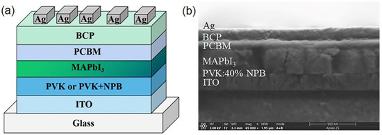
Figure 1.
The schematic diagram of device structure (a) and cross-sectional SEM image (b) of PSC.
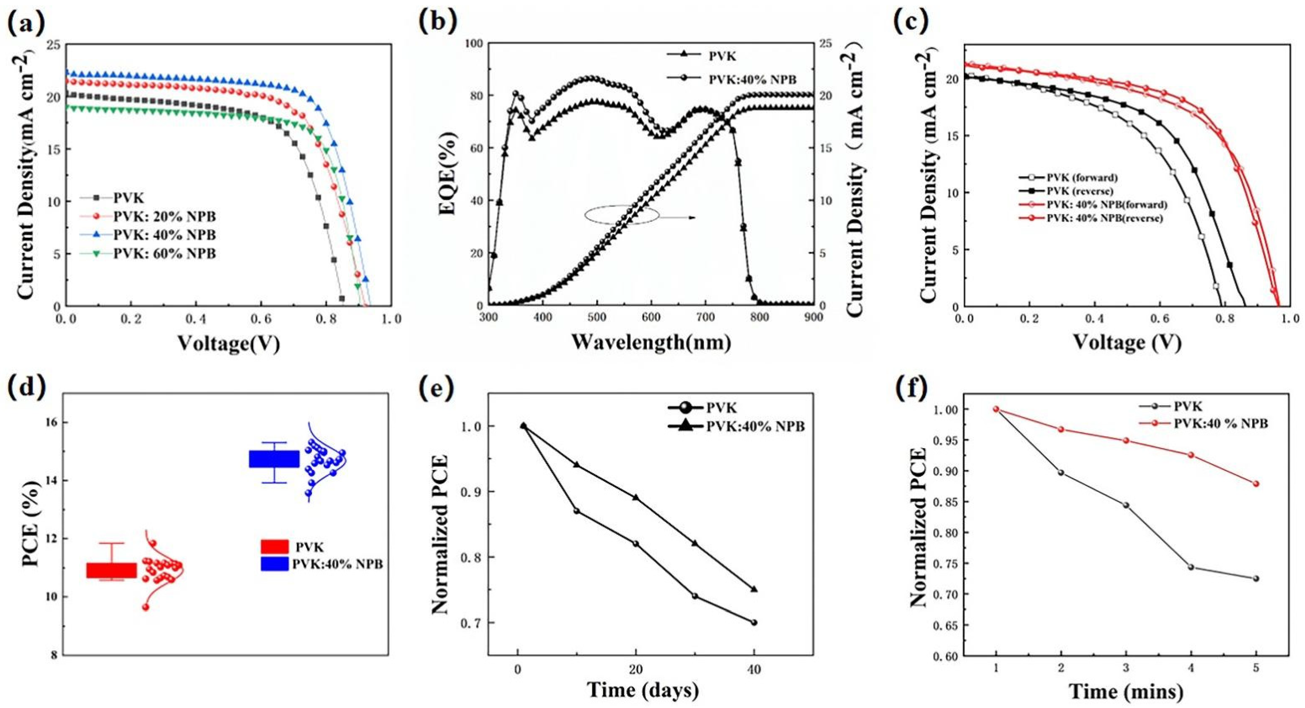
The current density–voltage (J–V) curves of PSCs are shown in Figure 2a, and the detailed performance parameters are summarized in Table 1. The results show that the PCE of the control device was 11.23% with a VOC of 0.85 V, a JSC of 20.23 mA cm−2, and an FF of 65.11%. After doping NPB in PVK, the PCE values of the PSCs all increased, which shows a dependence on the NPB concentration. When the weight ratio of NPB increased from 20% and 40% to 60%, the PCE values of the PSCs first increased to 13.16% and 15.04%, then decreased to 12.56%. The PSCs based on PVK doped with 40% NPB had the best performance with a VOC of 0.96 V, a JSC of 21.25 mA cm−2, and an FF of 70.03%. The resulting PCE of 15.05% is comparable with the highest PVK HTL-based PSCs, 15.8%, reported in the literature [21]. The enhancement of PCE values was caused by the simultaneous significant improvement of the VOC, JSC, and FF values. To further verify the promotion of JSC, the monochromatic incident photon-to-current conversion efficiency (IPCE) spectra of the control device and device based on PVK: 40% NPB were collected, as depicted in Figure 2b. It shows a stronger spectral response in 350-620 nm after the doping of 40% NPB. The integrated JSC values are 18.93 mA cm−2 and 20.13 mA cm−2 for the PVK and PVK:40% NPB-based PSC, respectively, and are in accordance with the JSC values obtained from the J–V scan as shown in Figure 2a and Table 1. The reverse and forward scanned J–V curves were compared for both the control device and the device based on PVK: 40% NPB HTL to illustrate the hysteresis effect of PSCs (Figure 2c). This demonstrated that NPB doping greatly reduced the J–V hysteresis of PSCs based on PVK HTL. In addition, to demonstrate the reliability of data, the PCE value statistics from 20 devices were shown in Figure 2d, which shows narrow distributions for both the control device and 40% NPB-doped device. The errors in Table 1 were obtained by dividing the difference between the best and the average values from 20 devices by 2.
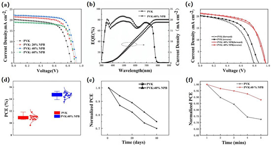
Figure 2.
(a) J–V curves of PSCs; (b) external quantum efficiency and integrated JSC of PSCs; (c) the reverse and forward scanned J–V curves of control device and device based on PVK: 40% NPB HTL; (d) PCE statistics of PSCs; (e) normalized PCE values during storage in glovebox filled with N2; and (f) stability of PSCs under continuous illustration by 1 sun (100 mW cm−2 AM 1.5 G).

Table 1.
Summary of detailed performance parameters of PSCs.
The storage stability of unencapsulated PSCs was evaluated through aging tests, as shown in Figure 2e. After 40 days storage in an N2-filled glovebox, the PCE of the control PSC decayed to 73.9% of the initial value, while it was 75.1% for the 40% NPB-doped device. This result suggests that NPB doping improved the device storage stability. The light stability of unencapsulated PSCs was also examined by collecting J–V data at one-minute intervals under continuous illustration by 1 sun (100 mW cm−2 AM 1.5 G). The change of PCE over time is shown in Figure 2f. After 5 min illustration, the PCE values were reduced to 73% and 88% of the initial values for the control device and the PVK:40% NPB HTL device, respectively. Apparently, the light stability of PSCs based on PVK:40% NPB HTL was better.
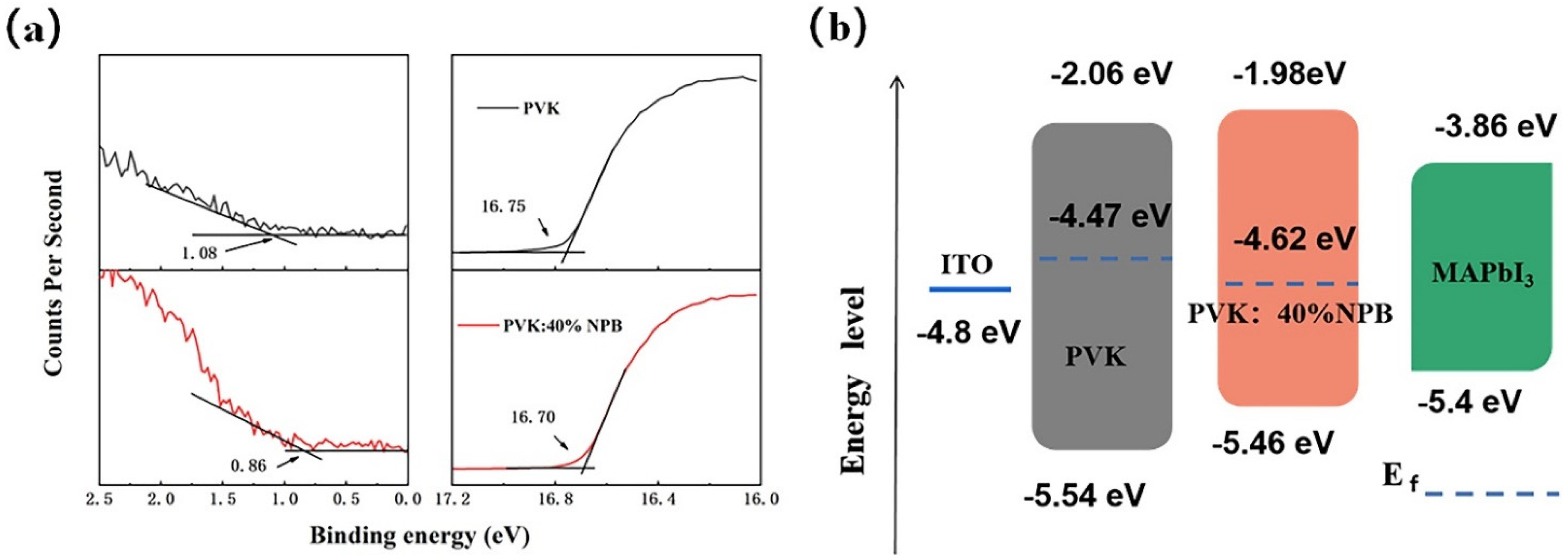
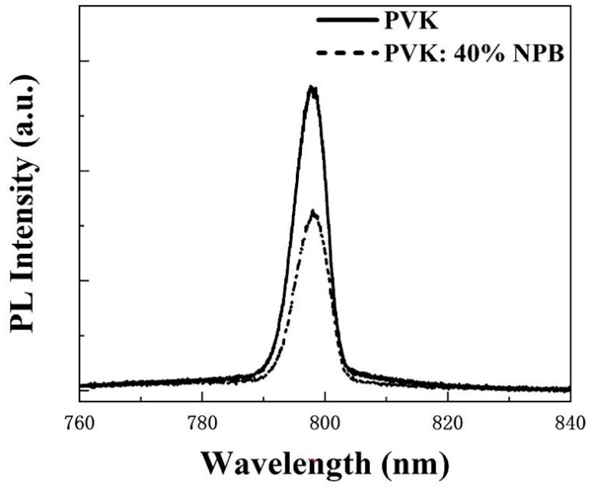
Ultraviolet photoelectron spectroscopy (UPS) was conducted to explore the influence of NPB doping on the electronic energy level of HTLs, as shown in Figure 3a. According to the secondary electron cutoff (Ecutoff) and Fermi edge (Eonset), the calculated highest occupied molecular orbital (HOMO) values are 5.54 eV and 5.46 eV for PVK and PVK: 40% NPB, respectively, as depicted in Figure 3b. Thus, after NPB doping, the energy gap between the HOMO of HTL and MAPbI3 was reduced from 0.14 eV to 0.06 eV. The improvement of energy alignment between HTL and MAPbI3 is mainly responsible for the increase in VOC after NPB doping [22]. This also suggests more efficient hole extraction efficiency, which contributed to the promotion of the JSC of PSCs. The PL spectra of MAPbI3 on different HTLs were measured, as shown in Figure 4. The lower PL intensity of MAPbI3 on PVK: 40% NPB HTL indicates more efficient hole extraction efficiency [23].
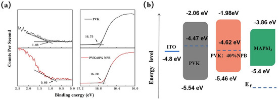
Figure 3.
(a) UPS of PVK and PVK:40% NPB films and (b) the corresponding energy band alignment.

Figure 4.
PL spectra of MAPbI3 on different HTLs.
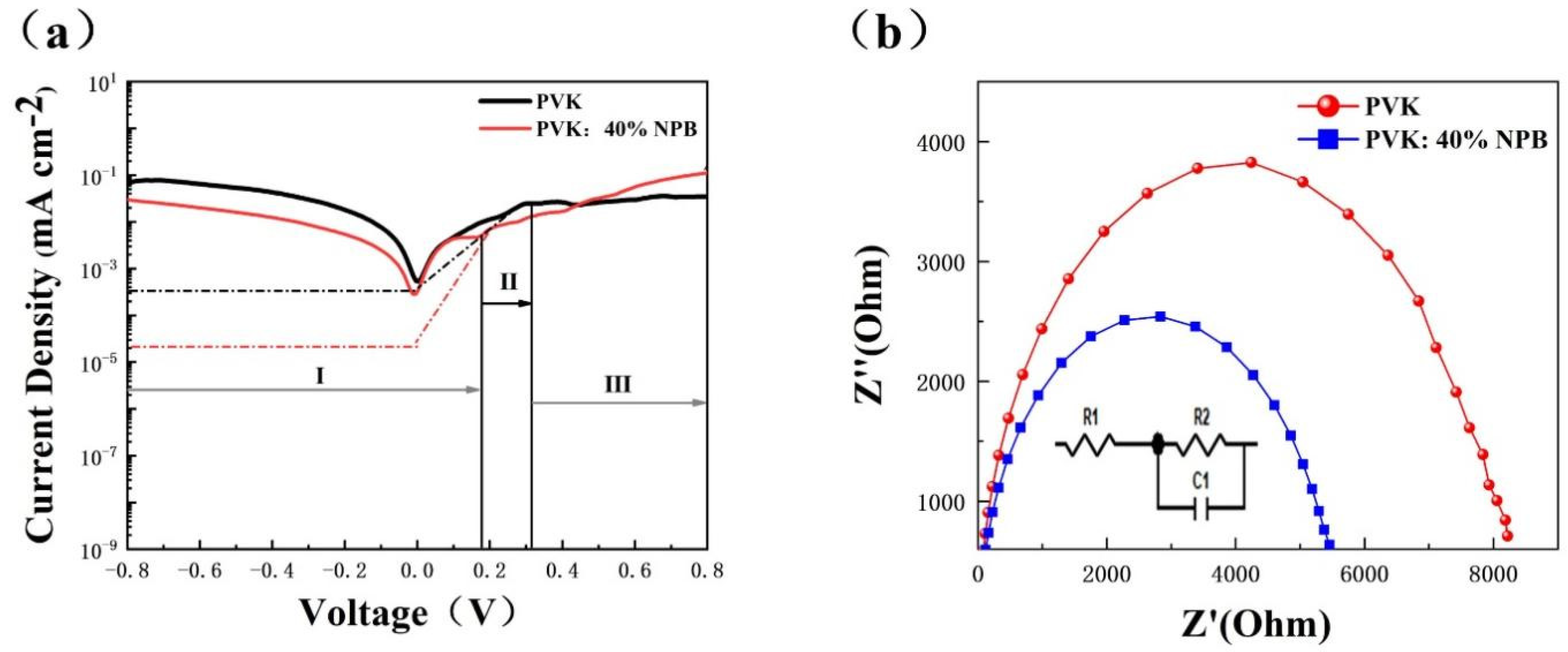
Dark J−V data were collected to investigate the charge carrier transport dynamic of PSCs. As shown in Figure 5a, dark J–V curves can be divided into three parts [24]. Region I is a straight line of the J−V curve between negative voltage and low positive voltage, which represents the leakage current. The slope is controlled by 1/ Rsh (shunt resistance). Region II is an exponential line at intermediate positive voltages, indicating that the J in region II is mainly composed of the diffusion current and the recombination current [25]. Region III is a straight line at high voltage, whose slope is controlled by 1/Rs (series resistance). In region I, the slope of the PVK: 40% NPB device is lower than that of the control device, which is reverse in region III. This implies a larger Rsh and smaller Rs of the PVK:40% NPB device. A larger Rsh corresponds to a higher VOC, and a smaller Rs will result in a higher JSC [26,27]. In region II, the reverse saturation current density (J0) can be evaluated from the intercept of the linear fitting in the exponential range, which is about 10−3 and 10−5 mA cm−2 for the control device and PVK: 40% NPB device, respectively. The exponent of the VOC is inversely proportional to J0 [28]. Thus, dark J–V curves suggest that the promotion of the VOC and JSC of PSCs after the addition of NPB in PVK can be ascribed to the decrease in Rs and J0 and the increase in Rsh.
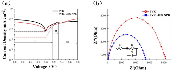
Figure 5.
(a) Dark J−V curves and (b) Nyquist plot of PSCs.
The electrochemical impedance spectroscopy (EIS) was also used to investigate the recombination inside PSCs. Figure 5b shows the Nyquist plot under dark conditions. The composite resistance (Rrec) of the PVK:40% NPB device is 9208/Ω, which is larger than 4166/Ω of the control device. The increase in Rrec indicates the suppressed charge carrier recombination inside the PSC [29,30].
3.2. Morphology and Properties of Perovskite Films
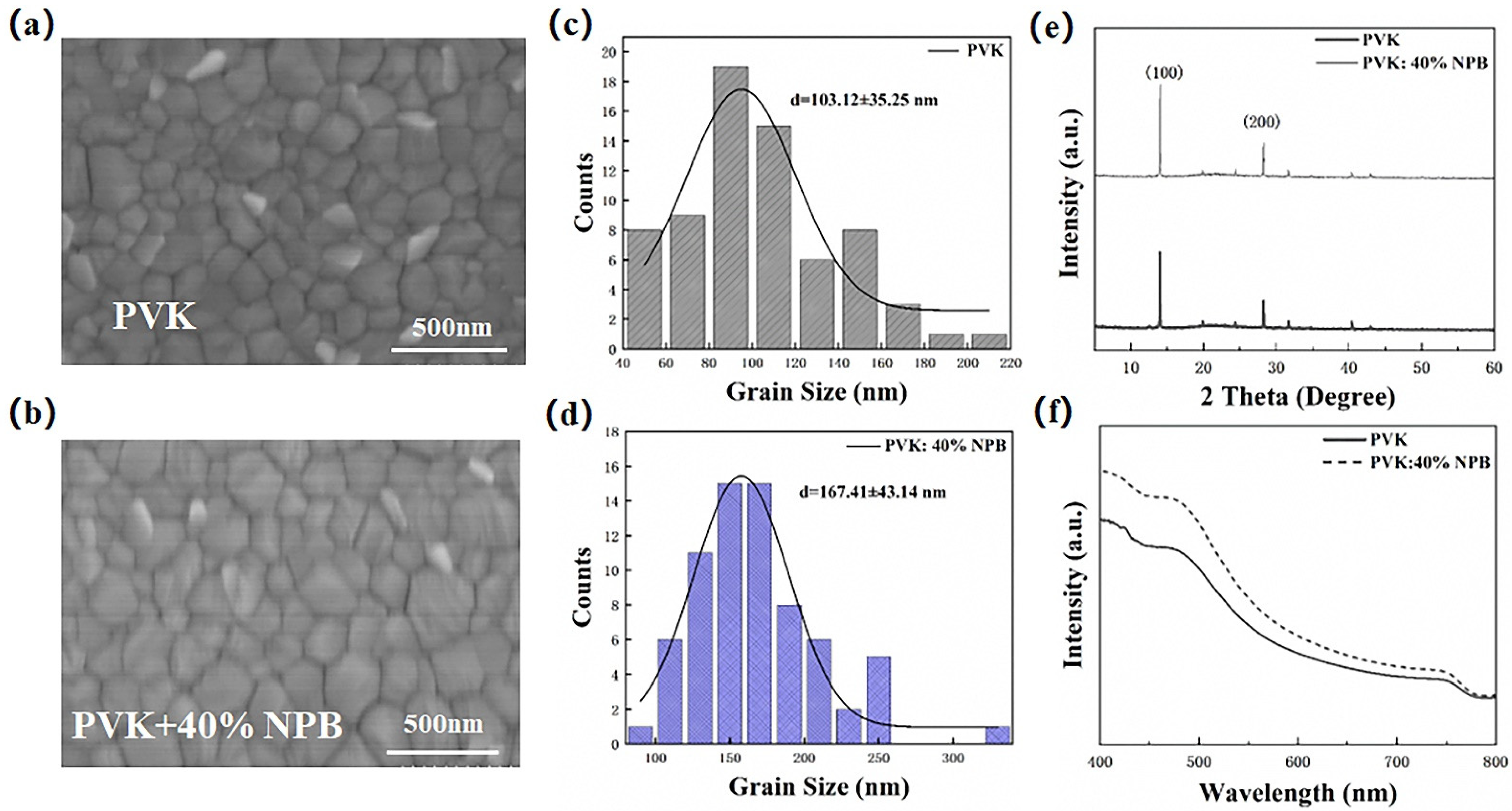
The morphology of the perovskite layer has a great influence on the performance of PSCs [31], which was then detected to explore the reason responsible for the performance enhancement of PSCs. Figure 6 shows the top-view SEM images of perovskite films on different HTLs. The corresponding grain size values were estimated by using Nano measure 1.2 and are depicted in Figure 6c,d. The average grain size of perovskite on pristine PVK HTL was 103 nm, which increased to 167 nm on PVK: 40% NPB. A larger grain size of the perovskite layer is usually caused by the increased crystallinity, which was then verified by collecting XRD patterns of perovskite films. It can be seen from Figure 6e that both patterns show characteristic peaks of orthogonal crystal structure of MAPbI3 at 14.1° and 28.2°, suggesting the unchanged growth direction of the MAPbI3 crystal, while the absolute intensities of both the (110) and (220) peaks of MAPbI3 on PVK: 40%NPB films are obviously higher than that of the pristine one, indicating the enhanced crystallinity of MAPbI3. The ultraviolet–visible (UV–Vis) absorption spectra of perovskite films deposited on different HTLs in Figure 6f show an increased absorption intensity in the range of 400–800 nm after NPB doping. This can be ascribed to perovskite crystallinity improvement [32]. The enhanced light absorption is one of the reasons responsible for the increase in JSC.
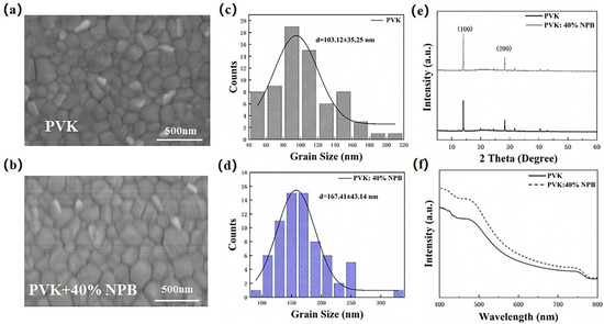
Figure 6.
Top-view SEM images and the corresponding grain size distribution of MAPbI3 film on top of (a,c) PVK and (b,d) PVK: 40% NPB; (e) XRD patterns and (f) UV–vis absorption spectra of MAPbI3 films.
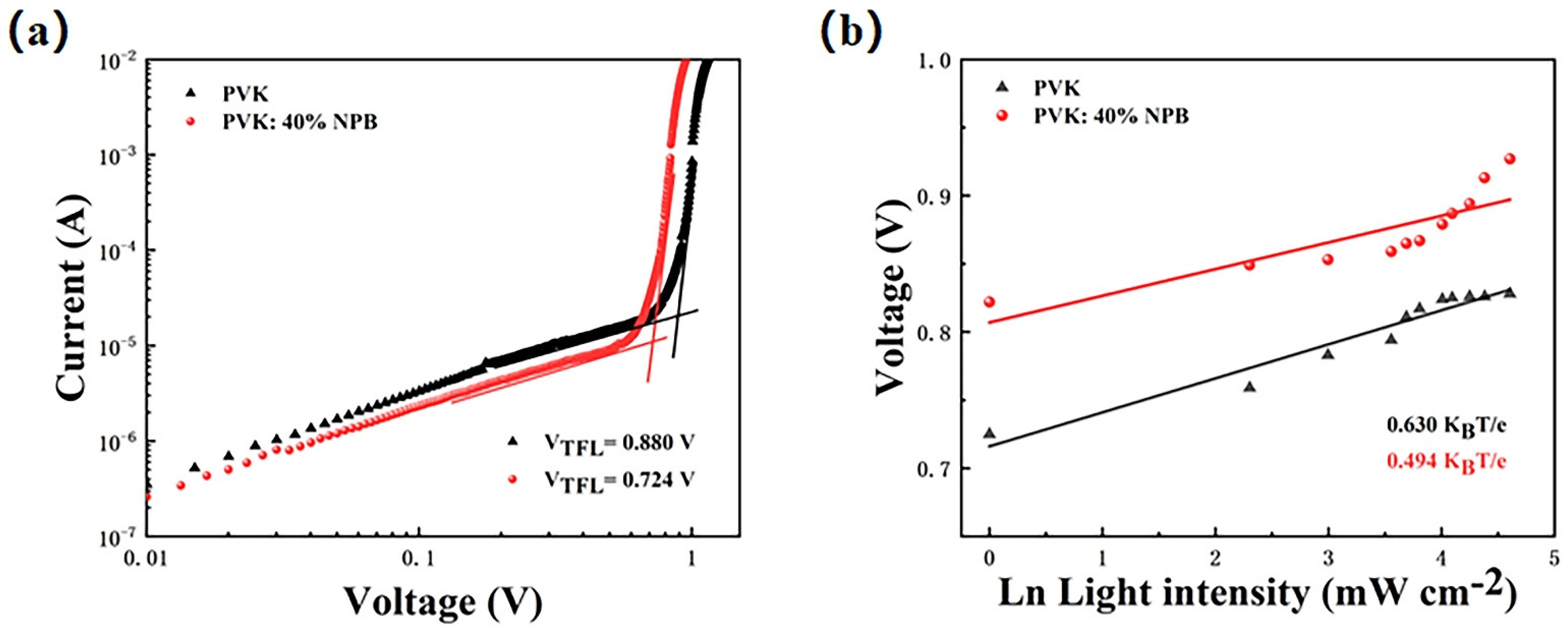
The perovskite film with the large grain size contains less defect density of state, which can be estimated by using J–V curve of a single-carrier device. Thus, the hole-only device with a structure of ITO/HTL/MAPbI3 (260 nm)/PTAA (25 nm)/Ag (100 nm) was prepared. The density of defects can be calculated by formula (1) [33,34]:
where ε is the dielectric constant, ε0 is the vacuum dielectric constant, q is the elementary charge, and L is the thickness of the perovskite layer. VTFL is the voltage at the node of the J–V curve in Figure 7a, which is the trap-filling limit voltage. It can be seen from the figure that the current density increases rapidly when the bias voltage exceeds the node. This shows that the defect state is almost completely filled. The VTFL values are 0.880 V and 0.724 V for the control and PVK: 40% NPB devices, respectively. The corresponding Ndefect values are estimated to be 3.5 × 10¹⁶ and 2.9 × 1016 cm−3, respectively. The reduction of the defect density is beneficial to suppress the recombination of carriers, which is consistent with the result obtained by the EIS test. The dependence of VOC on light intensity was also tested to deeply explore the carrier recombination process caused by the defect state in the optoelectronic device. Figure 7b shows the scatter plot of VOC with respect to ln(I), according to the following formula (2) [35]:
where n is the ideal factor, KB is Boltzmann’s constant, q is the elementary charge, T is the absolute temperature, and I is the light intensity. The slope of the line after fitting in the figure is n (KBT e−1), which is 0.630 and 0.494 KBT e−1 for the control and PVK:40% NPB device, respectively [36]. The decrease in the slope value means that NPB doping can effectively reduce the trap-assisted carrier recombination [37], which is in accordance with the above results.
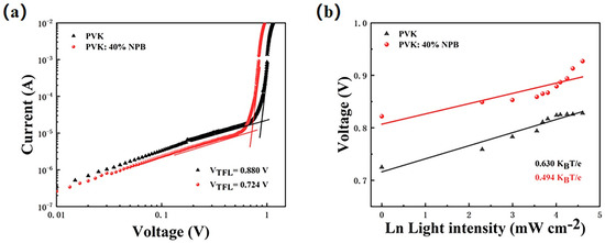
Figure 7.
(a) Hole-only device based on different HTLs; (b) light intensity dependence of VOC. The light intensity increased from 1 to 100 mW cm−2.
3.3. Working Mechanism Analysis
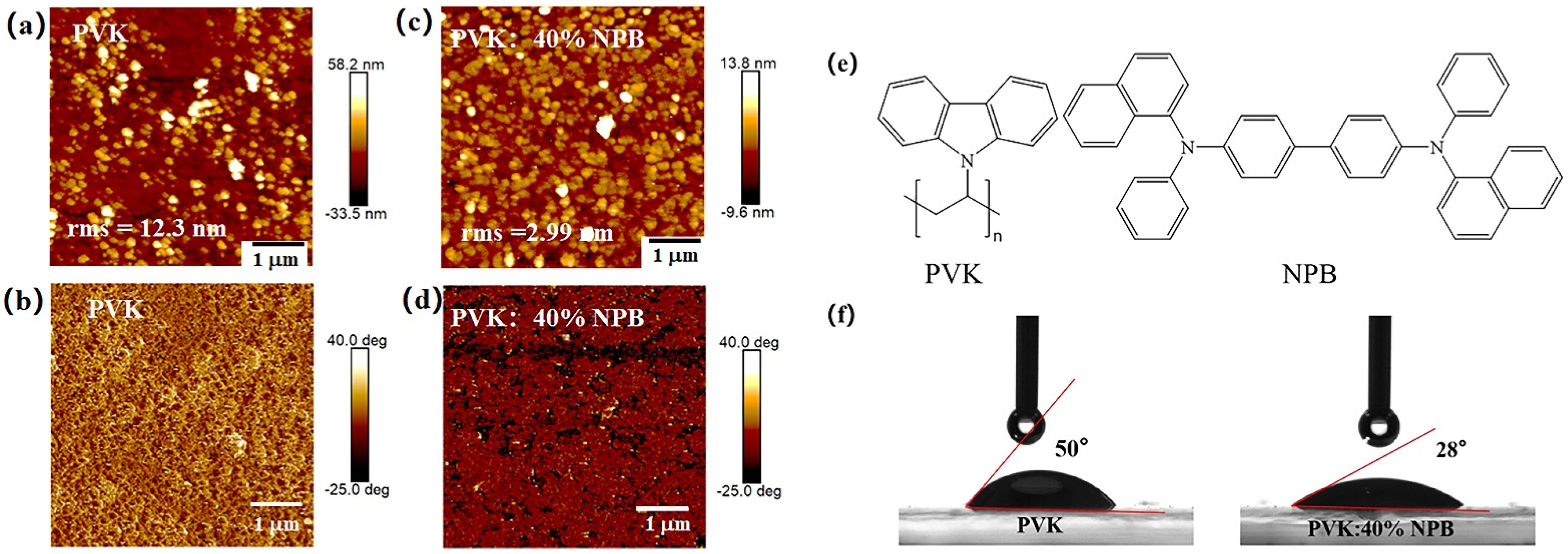
The morphology improvement of the MAPbI3 layer with a larger grain size and less defect density induced the promotion of PCE of PSCs. To explore the reason responsible for the morphology improvement of MAPbI3, the surface topography of HTL layers was observed by using AFM, as shown in Figure 8. After adding 40% NPB in PVK, the root mean-square (rms) roughness of the HTL decreased from 12.3 nm to 2.99 nm. A smoother surface of HTL would decrease the nucleation sites for perovskite to grow and provide a better contact with the perovskite layer [38]. The C–H… π interaction between methyl groups in the PVK and the phenyl rings in the NPB interlaces with π−π stacking chains resulted in a packing motif quite similar to the conformation of polymer chains (Figure 8e). Thus, the intermolecular aggregation in the PVK was suppressed [39]. PVK chains were well dispersed within the NPB matrix due to the similar repeating unit between them, leading to a flat and smooth surface [40,41].

Figure 8.
AFM images of HTLs: (a,c) height images and (b,d) phase images; (e) molecular structure of PVK and NPB; and (f) contact angles of perovskite precursor solution on HTLs.
The contact angles of the MAPbI3 precursor solution on different HTL films were measured as shown in Figure 8f. For the pristine PVK substrate, the contact angle is about 50°, whereas it is 28° for the NPB-doped PVK, indicating the increased wettability. Good wettability of the perovskite precursor solution on the substrate is beneficial for the crystallization of perovskite film [42].
4. Discussion
With the NPB in PVK, the energy gap between the HOMO of HTL and MAPbI3 was reduced, leading to the enhancement of the VOC. The smoother surface and better hydrophilicity of the NPB-doped HTL gave rise to the morphology improvement of MAPbI3. MAPbI3 film with a larger grain size and less defect density was obtained. The reduction of Rs and increase in Rsh and UV–Vis absorption intensity are mainly responsible for the enhancement of JSC and FF. Finally, a PCE promotion from 11.23% to 15.04% was achieved. This work demonstrates the great potential of PVK HTL-based PSCs.
Supplementary Materials
The following supporting information can be downloaded at: https://www.mdpi.com/article/10.3390/polym14112249/s1, Figure S1: PSCs based on PVK: (a) different concentration and fixed spin-coating speed of 4000 rpm and (b) fixed concentration of 1 mg/mL and different spin-coating speed; Table S1: Summary of the detailed performance parameters of PSCs based on PVK with different concentration or spin-coating speed.
Author Contributions
Conceptualization, Y.M. (Yuhui Ma); methodology, C.Y.; software, W.H.; validation, L.Z.; investigation, Y.X. and L.Z.; resources, W.Z. and J.H.; data curation, L.Z.; writing—original draft preparation, Y.X.; writing—review and editing, Q.N.; supervision, Q.N.; project administration, Q.N.; funding acquisition, Y.M. (Yonggang Min) and R.X. All authors have read and agreed to the published version of the manuscript.
Funding
This research was funded by the National Natural Science Foundation of China (Grant Numbers: 61874058, 51861145301), the Natural Science Foundation of NUPTSF (Grant Numbers: NY215077, NY215022, NY220059), and the Science and Technology Program of Guangzhou (Grant Number: 201804020005).
Institutional Review Board Statement
Not applicable.
Informed Consent Statement
Not applicable.
Data Availability Statement
Data sharing not applicable.
Acknowledgments
Many thanks to Wang Lei from Nanjing Normal University for testing the cross-sectional SEM images of perovskite film.
Conflicts of Interest
The authors declare no conflict of interest.
References
- Huang, L.; Wu, L.; Sun, Q.; Jin, C.; Wang, J.; Fu, S.; Wu, Z.; Liu, X.; Hu, Z.; Zhang, J. All in One: A Versatile n-Perovskite/p-Spiro-MeOTAD p–n Heterojunction Diode as a Photovoltaic Cell, Photodetector, and Memristive Photosynapse. J. Phys. Chem. Lett. 2021, 12, 12098–12106. [Google Scholar] [CrossRef]
- Kong, T.; Xie, H.; Zhang, Y.; Song, J.; Li, Y.; Lim, E.L.; Hagfeldt, A.; Bi, D. Perovskitoid-Templated Formation of a 1D@ 3D Perovskite Structure toward Highly Efficient and Stable Perovskite Solar Cells. Adv. Energy Mater. 2021, 11, 2101018. [Google Scholar] [CrossRef]
- Li, N.; Jia, Y.; Guo, Y.; Zhao, N. Ion Migration in Perovskite Light Emitting Diodes: Mechanism, Characterizations, and Material and Device Engineering. Adv. Mater. 2021, 34, 2108102. [Google Scholar] [CrossRef] [PubMed]
- Kojima, A.; Teshima, K.; Shirai, Y.; Miyasaka, T. Organometal halide perovskites as visible-light sensitizers for photovoltaic cells. J. Am. Chem. Soc. 2009, 131, 6050–6051. [Google Scholar] [CrossRef]
- Goetz, K.P.; Taylor, A.D.; Hofstetter, Y.J.; Vaynzof, Y. Sustainability in perovskite solar cells. ACS Appl. Mater. Interfaces 2021, 13, 1–17. [Google Scholar] [CrossRef]
- Ma, F.; Zhao, Y.; Li, J.; Zhang, X.; Gu, H.; You, J. Nickel oxide for inverted structure perovskite solar cells. J. Energy Chem. 2021, 52, 393–411. [Google Scholar] [CrossRef]
- Mei, A.; Li, X.; Liu, L.; Ku, Z.; Liu, T.; Rong, Y.; Xu, M.; Hu, M.; Chen, J.; Yang, Y. A hole-conductor–free, fully printable mesoscopic perovskite solar cell with high stability. Science 2014, 345, 295–298. [Google Scholar] [CrossRef] [PubMed]
- Heo, J.H.; Song, D.H.; Han, H.J.; Kim, S.Y.; Kim, J.H.; Kim, D.; Shin, H.W.; Ahn, T.K.; Wolf, C.; Lee, T.W. Planar CH3NH3PbI3 perovskite solar cells with constant 17.2% average power conversion efficiency irrespective of the scan rate. Adv. Mater. 2015, 27, 3424–3430. [Google Scholar] [CrossRef]
- Zhou, W.; Wen, Z.; Gao, P. Less is more: Dopant-free hole transporting materials for high-efficiency perovskite solar cells. Adv. Energy Mater. 2018, 8, 1702512. [Google Scholar] [CrossRef]
- Wu, F.; Yan, K.; Wu, H.; Niu, B.; Liu, Z.; Li, Y.; Zuo, L.; Chen, H. Tuning interfacial chemical interaction for high-performance perovskite solar cell with PEDOT: PSS as hole transporting layer. J. Mater. Chem. A 2021, 9, 14920–14927. [Google Scholar] [CrossRef]
- Li, B.; Yang, K.; Liao, Q.; Wang, Y.; Su, M.; Li, Y.; Shi, Y.; Feng, X.; Huang, J.; Sun, H. Imide-Functionalized Triarylamine-Based Donor-Acceptor Polymers as Hole Transporting Layers for High-Performance Inverted Perovskite Solar Cells. Adv. Funct. Mater. 2021, 31, 2100332. [Google Scholar] [CrossRef]
- Girotto, C.; Moia, D.; Rand, B.P.; Heremans, P. High-performance organic solar cells with spray-coated hole-transport and active layers. Adv. Funct. Mater. 2011, 21, 64–72. [Google Scholar]
- Guerrero, A.; You, J.; Aranda, C.; Kang, Y.S.; Garcia-Belmonte, G.; Zhou, H.; Bisquert, J.; Yang, Y. Interfacial degradation of planar lead halide perovskite solar cells. ACS Nano 2016, 10, 218–224. [Google Scholar] [CrossRef] [PubMed]
- Jeon, N.J.; Noh, J.H.; Kim, Y.C.; Yang, W.S.; Ryu, S.; Seok, S.I. Solvent engineering for high-performance inorganic-organic hybrid perovskite solar cells. Nat. Mater. 2014, 139, 897–903. [Google Scholar] [CrossRef]
- Xu, B.; Sheibani, E.; Liu, P.; Zhang, J.; Tian, H.; Vlachopoulos, N.; Boschloo, G.; Kloo, L.; Hagfeldt, A.; Sun, L. Carbazole-based hole-transport materials for efficient solid-state dye-sensitized solar cells and perovskite solar cells. Adv. Mater. 2014, 26, 6629–6634. [Google Scholar] [CrossRef]
- Deschler, F.; Riedel, D.; Ecker, B.; von Hauff, E.; Da Como, E.; MacKenzie, R.C. Increasing organic solar cell efficiency with polymer interlayers. Phys. Chem. Chem. Phys. 2013, 15, 764–769. [Google Scholar] [CrossRef] [Green Version]
- Meerholz, K.; Bittner, R.; De Nardin, Y.; Bräuchle, C.; Hendrickx, E.; Volodin, B.L.; Kippelen, B.; Peyghambarian, N. Stability improvement of high-performance photorefractive polymers containing eutectic mixtures of electro-optic chromophores. Adv. Mater. 1997, 9, 1043–1046. [Google Scholar] [CrossRef]
- Ou, L.; Han, S.; Ding, W.; Chen, Z.; Ye, Z.; Yang, H.; Zhang, G.; Lou, Y.; Chen, J.-Z.; Yu, Y. Design, synthesis and 3D-QSAR study of cytotoxic flavonoid derivatives. Mol. Divers. 2011, 15, 665–675. [Google Scholar] [CrossRef]
- Mann, D.S.; Patil, P.; Kim, D.-H.; Kwon, S.-N.; Na, S.-I. Boron nitride-incorporated NiOx as a hole transport material for high-performance pin planar perovskite solar cells. J. Power Sources 2020, 477, 228738. [Google Scholar] [CrossRef]
- Geffroy, C.; Grana, E.; Mumtaz, M.; Cojocaru, L.; Hadziioannou, G. Post-functionalization of polyvinylcarbazoles: An open route towards hole transporting materials for perovskite solar cells. Sol. Energy 2019, 193, 878–884. [Google Scholar] [CrossRef]
- Yang, L.; Yan, Y.; Cai, F.; Li, J.; Wang, T. Poly (9-vinylcarbazole) as a hole transport material for efficient and stable inverted planar heterojunction perovskite solar cells. Sol. Energy Mater. Sol. Cells 2017, 163, 210–217. [Google Scholar] [CrossRef]
- Klein, A.; Jaegermann, W. Fermi-level-dependent defect formation in Cu-chalcopyrite semiconductors. Appl. Phys. Lett. 1999, 74, 2283–2285. [Google Scholar] [CrossRef]
- Li, Y.; Wang, B.; Liu, T.; Zeng, Q.; Cao, D.; Pan, H.; Xing, G. Interfacial Engineering of PTAA/Perovskites for Improved Crystallinity and Hole Extraction in Inverted Perovskite Solar Cells. ACS Appl. Mater. Interfaces 2022, 14, 3284–3292. [Google Scholar] [CrossRef] [PubMed]
- Savva, A.; Burgués-Ceballos, I.; Choulis, S.A. Improved Performance and Reliability of p-i-n Perovskite Solar Cells via Doped Metal Oxides. Adv. Energy Mater. 2016, 6, 1600285. [Google Scholar]
- Ma, Y.; Zhang, H.; Zhang, Y.; Hu, R.; Jiang, M.; Zhang, R.; Lv, H.; Tian, J.; Chu, L.; Zhang, J. Enhancing the performance of inverted perovskite solar cells via grain boundary passivation with carbon quantum dots. ACS Appl. Mater. Interfaces 2018, 11, 3044–3052. [Google Scholar] [CrossRef]
- Zhang, H.; Azimi, H.; Hou, Y.; Ameri, T.; Przybilla, T.; Spiecker, E.; Kraft, M.; Scherf, U.; Brabec, C.J. Improved High-Efficiency Perovskite Planar Heterojunction Solar Cells via Incorporation of a Polyelectrolyte Interlayer. Chem. Mater. 2014, 26, 5190–5193. [Google Scholar] [CrossRef]
- Zhang, F.; Song, J.; Hu, R.; Xiang, Y.; He, J.; Hao, Y.; Lian, J.; Zhang, B.; Zeng, P.; Qu, J. Interfacial Passivation of the p-Doped Hole-Transporting Layer Using General Insulating Polymers for High-Performance Inverted Perovskite Solar Cells. Small 2018, 14, 1704007. [Google Scholar] [CrossRef]
- Xue, Q.; Liu, M.; Li, Z.; Yan, L.; Hu, Z.; Zhou, J.; Li, W.; Jiang, X.-F.; Xu, B.; Huang, F.; et al. Efficient and Stable Perovskite Solar Cells via Dual Functionalization of Dopamine Semiquinone Radical with Improved Trap Passivation Capabilities. Adv. Funct. Mater. 2018, 28, 1707444. [Google Scholar] [CrossRef]
- Miyano, K.; Tripathi, N.; Yanagida, M.; Shirai, Y. Lead Halide Perovskite Photovoltaic as a Model p–i–n Diode. Acc. Chem. Res. 2016, 49, 303–310. [Google Scholar]
- Kim, H.S.; Mora-Sero, I.; Gonzalez-Pedro, V.; Fabregat-Santiago, F.; Juarez-Perez, E.J.; Park, N.G.; Bisquert, J. Mechanism of carrier accumulation in perovskite thin-absorber solar cells. Nat. Commun. 2013, 4, 2242. [Google Scholar] [CrossRef] [Green Version]
- Sin, D.H.; Ko, H.; Jo, S.B.; Kim, M.; Bae, G.Y.; Cho, K. Decoupling Charge Transfer and Transport at Polymeric Hole Transport Layer in Perovskite Solar Cells. ACS Appl. Mater. Interfaces 2016, 8, 6546–6553. [Google Scholar] [CrossRef] [PubMed]
- Jiang, Z.; Chen, X.; Lin, X.; Jia, X.; Wang, J.; Pan, L.; Huang, S.; Zhu, F.; Sun, Z. Amazing stable open-circuit voltage in perovskite solar cells using AgAl alloy electrode. Sol. Energy Mater. Sol. Cells 2016, 146, 35–43. [Google Scholar] [CrossRef]
- Chen, C.; Liu, D.; Wu, Y.; Bi, W.; Sun, X.; Chen, X.; Liu, W.; Xu, L.; Song, H.; Dai, Q. Dual interfacial modifications by conjugated small-molecules and lanthanides doping for full functional perovskite solar cells. Nano Energy 2018, 53, 849–862. [Google Scholar] [CrossRef]
- Chen, C.; Liu, D.; Zhang, B.; Bi, W.; Li, H.; Jin, J.; Chen, X.; Xu, L.; Song, H.; Dai, Q. Carrier interfacial engineering by bismuth modification for efficient and thermoresistant perovskite solar cells. Adv. Energy Mater. 2018, 8, 1703659. [Google Scholar] [CrossRef]
- Tripathi, N.; Shirai, Y.; Yanagida, M.; Karen, A.; Miyano, K. Novel surface passivation technique for low-temperature solution-processed perovskite PV cells. ACS Appl. Mater. Interfaces 2016, 8, 4644–4650. [Google Scholar] [CrossRef]
- He, Z.; Xiao, B.; Liu, F.; Wu, H.; Yang, Y.; Xiao, S.; Wang, C.; Russell, T.P.; Cao, Y. Single-junction polymer solar cells with high efficiency and photovoltage. Nat. Photonics 2015, 9, 174–179. [Google Scholar] [CrossRef]
- Wu, Y.; Li, X.; Fu, S.; Wan, L.; Fang, J. Efficient methylammonium lead trihalide perovskite solar cells with chloroformamidinium chloride (Cl-FACl) as an additive. J. Mater. Chem. A 2019, 7, 8078–8084. [Google Scholar] [CrossRef]
- Deng, Y.; Peng, E.; Shao, Y.; Xiao, Z.; Dong, Q.; Huang, J. Scalable fabrication of efficient organolead trihalide perovskite solar cells with doctor-bladed active layers. Energy Environ. Sci. 2015, 8, 1544–1550. [Google Scholar] [CrossRef]
- Qiao, J.; Wang, L.D.; Xie, J.F.; Lei, G.T.; Wu, G.S.; Qiu, Y. Strongly luminescent binuclear aluminium chelate with polymer-like molecular packing and solution-processibility. Chem. Commun. 2005, 36, 4560–4562. [Google Scholar] [CrossRef]
- Ball, J.M.; Petrozza, A. Defects in perovskite-halides and their effects in solar cells. Nat. Energy 2016, 1, 16149. [Google Scholar] [CrossRef]
- Huang, X.; Wang, K.; Yi, C.; Meng, T.; Gong, X. Efficient perovskite hybrid solar cells by highly electrical conductive PEDOT: PSS hole transport layer. Adv. Energy Mater. 2016, 6, 1501773. [Google Scholar] [CrossRef]
- Li, X.; Zhao, X.; Hao, F.; Yin, X.; Yao, Z.; Zhou, Y.; Shen, H.; Lin, H. Bifacial modified charge transport materials for highly efficient and stable inverted perovskite solar cells. ACS Appl. Mater. Interfaces 2018, 10, 17861–17870. [Google Scholar] [CrossRef] [PubMed]

Publisher’s Note: MDPI stays neutral with regard to jurisdictional claims in published maps and institutional affiliations. |
© 2022 by the authors. Licensee MDPI, Basel, Switzerland. This article is an open access article distributed under the terms and conditions of the Creative Commons Attribution (CC BY) license (https://creativecommons.org/licenses/by/4.0/).