
Variable Direct Electromechanical Properties of As-Electrospun Polystyrene Microfiber Mats with Different Electrospinning Conditions


Abstract
:
1. Introduction
2. Materials and Methods
2.1. Materials and Fabrication of the Fiber Mats
2.2. Morphological and Electrical Characterization
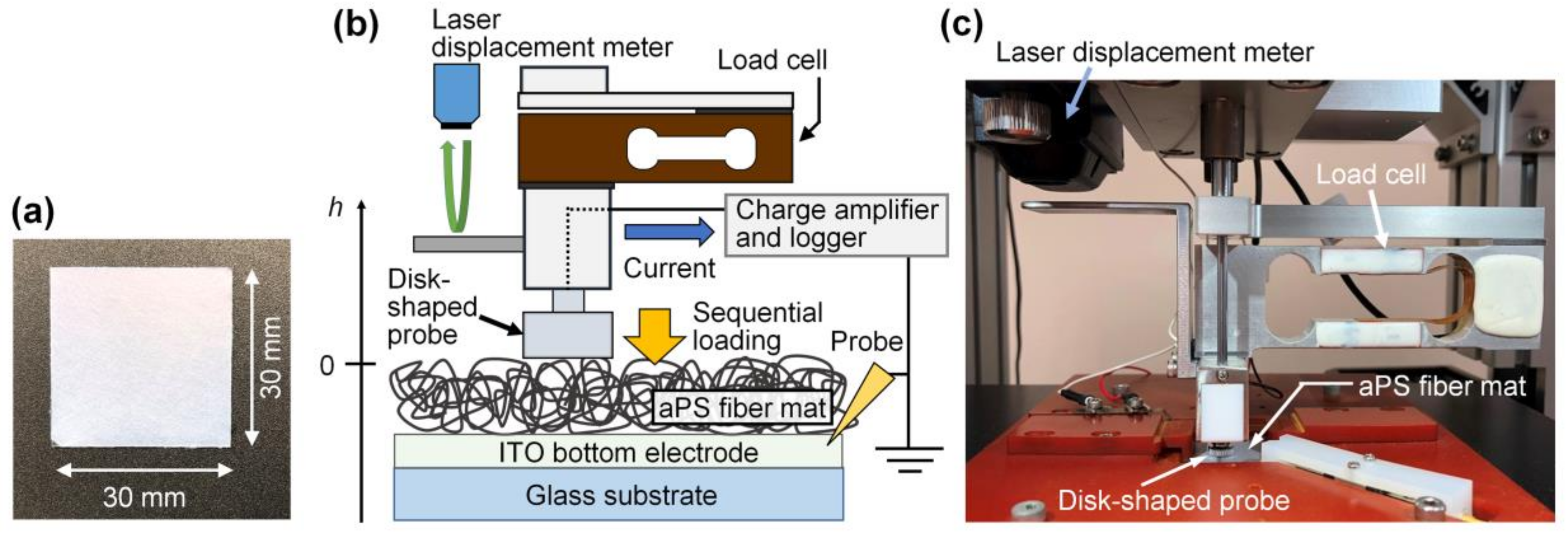
2.3. Quasistatic Direct Electromechanical Characterization
2.4. Electrostatic Characterization
3. Results and Discussion
3.1. Geometrical Characteristics
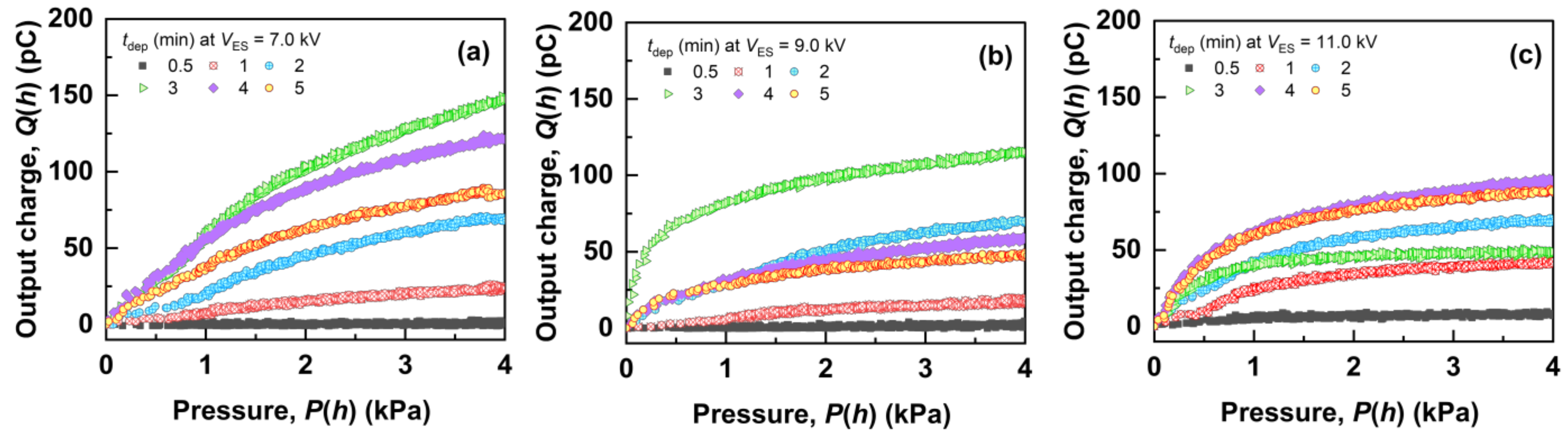
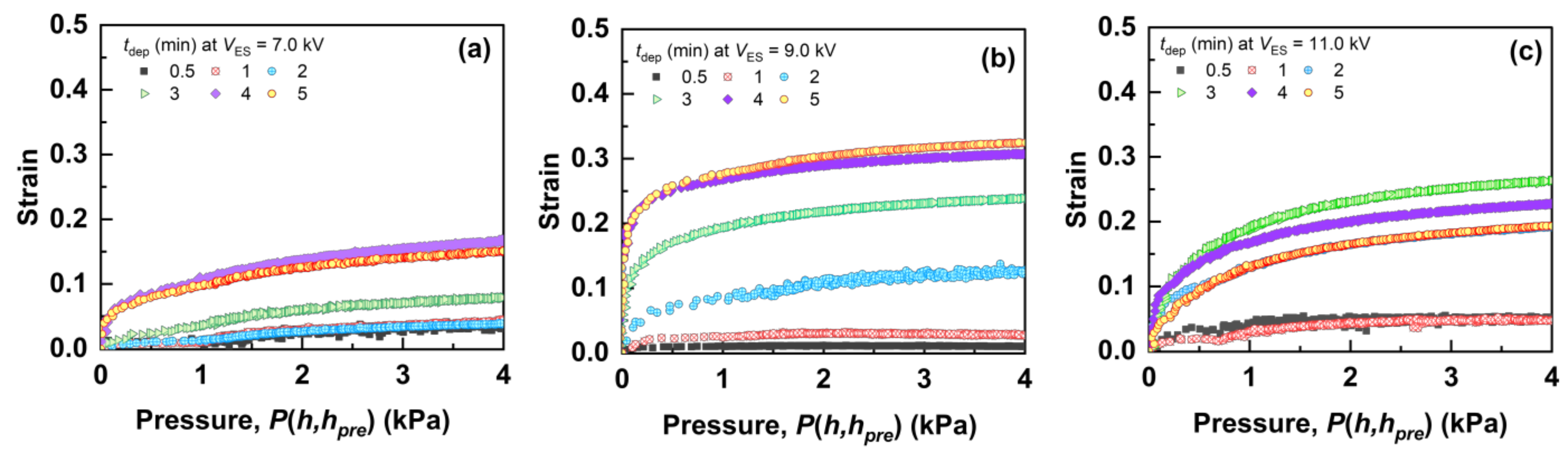
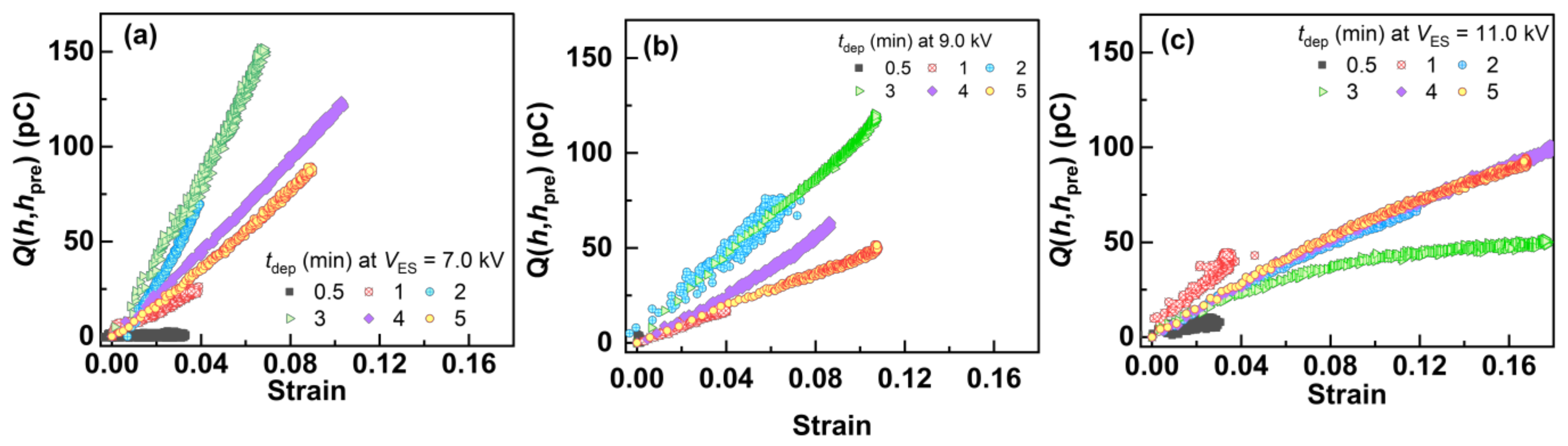
3.2. Direct Electromechanical Characteristics
3.3. Charge Distribution in the Fiber Mat
3.4. Structure Inside the Fiber Mat
4. Conclusions
Supplementary Materials
Author Contributions
Funding
Institutional Review Board Statement
Informed Consent Statement
Data Availability Statement
Acknowledgments
Conflicts of Interest
References
- Jayathilaka, W.A.D.M.; Qi, K.; Qin, Y.; Chinnappan, A.; Serrano-García, W.; Baskar, C.; Wang, H.; He, J.; Cui, S.; Thomas, S.W.; et al. Significance of Nanomaterials in Wearables: A Review on Wearable Actuators and Sensors. Adv. Mater. 2019, 31, 1805921. [Google Scholar] [CrossRef]
- Mokhtari, F.; Cheng, Z.; Raad, R.; Xi, J.; Foroughi, J. Piezofibers to smart textiles: A review on recent advances and future outlook for wearable technology. J. Mater. Chem. A 2020, 8, 9496–9522. [Google Scholar] [CrossRef]
- Amjadi, M.; Kyung, K.U.; Park, I.; Sitti, M. Stretchable, Skin-Mountable, and Wearable Strain Sensors and Their Potential Applications: A Review. Adv. Funct. Mater. 2016, 26, 1678–1698. [Google Scholar] [CrossRef]
- Liu, Y.; Pharr, M.; Salvatore, G.A. Lab-on-Skin: A Review of Flexible and Stretchable Electronics for Wearable Health Monitoring. ACS Nano 2017, 11, 9614–9635. [Google Scholar] [CrossRef] [PubMed]
- Chen, W.; Yan, X. Progress in achieving high-performance piezoresistive and capacitive flexible pressure sensors: A review. J. Mater. Sci. Technol. 2020, 43, 175–188. [Google Scholar] [CrossRef]
- Liu, Y.; He, K.; Chen, G.; Leow, W.R.; Chen, X. Nature-Inspired Structural Materials for Flexible Electronic Devices. Chem. Rev. 2017, 117, 12893–12941. [Google Scholar] [CrossRef] [PubMed]
- Khan, Y.; Ostfeld, A.E.; Lochner, C.M.; Pierre, A.; Arias, A.C. Monitoring of Vital Signs with Flexible and Wearable Medical Devices. Adv. Mater. 2016, 28, 4373–4395. [Google Scholar] [CrossRef]
- Kwon, D.; Lee, T.I.; Shim, J.; Ryu, S.; Kim, M.S.; Kim, S.; Kim, T.S.; Park, I. Highly Sensitive, Flexible, and Wearable Pressure Sensor Based on a Giant Piezocapacitive Effect of Three-Dimensional Microporous Elastomeric Dielectric Layer. ACS Appl. Mater. Int. 2016, 8, 16922–16931. [Google Scholar] [CrossRef]
- Mu, C.; Li, J.; Song, Y.; Huang, W.; Ran, A.; Deng, K.; Huang, J.; Xie, W.; Sun, R.; Zhang, H. Enhanced Piezocapacitive Effect in CaCu3Ti4O12-Polydimethylsiloxane Composited Sponge for Ultrasensitive Flexible Capacitive Sensor. ACS Appl. Nano Mater. 2018, 1, 274–283. [Google Scholar] [CrossRef]
- Yang, Y.; Zhang, H.; Lin, Z.H.; Zhou, Y.S.; Jing, Q.; Su, Y.; Yang, J.; Chen, J.; Hu, C.; Wang, Z.L. Human skin based triboelectric nanogenerators for harvesting biomechanical energy and as self-powered active tactile sensor system. ACS Nano 2013, 7, 9213–9222. [Google Scholar] [CrossRef] [Green Version]
- Wang, S.; Lin, L.; Wang, Z.L. Triboelectric nanogenerators as self-powered active sensors. Nano Energy 2015, 11, 436–462. [Google Scholar] [CrossRef] [Green Version]
- Fan, F.R.; Lin, L.; Zhu, G.; Wu, W.; Zhang, R.; Wang, Z.L. Transparent triboelectric nanogenerators and self-powered pressure sensors based on micropatterned plastic films. Nano Lett. 2012, 12, 3109–3114. [Google Scholar] [CrossRef] [PubMed] [Green Version]
- Gee, S.; Johnson, B.; Smith, A.L. Optimizing electrospinning parameters for piezoelectric PVDF nanofiber membranes. J. Membr. Sci. 2018, 563, 804–812. [Google Scholar] [CrossRef]
- Yousry, Y.M.; Yao, K.; Chen, S.; Liew, W.H.; Ramakrishna, S. Mechanisms for Enhancing Polarization Orientation and Piezoelectric Parameters of PVDF Nanofibers. Adv. Electron. Mater. 2018, 4, 1700562. [Google Scholar] [CrossRef]
- Persano, L.; Dagdeviren, C.; Su, Y.; Zhang, Y.; Girardo, S.; Pisignano, D.; Huang, Y.; Rogers, J.A. High performance piezoelectric devices based on aligned arrays of nanofibers of poly(vinylidenefluoride-co-trifluoroethylene). Nat. Commun. 2013, 4, 1610–1633. [Google Scholar] [CrossRef]
- Wu, N.; Cheng, X.; Zhong, Q.; Zhong, J.; Li, W.; Wang, B.; Hu, B.; Zhou, J. Cellular Polypropylene Piezoelectret for Human Body Energy Harvesting and Health Monitoring. Adv. Funct. Mater. 2015, 25, 4788–4794. [Google Scholar] [CrossRef]
- Chu, Y.; Zhong, J.; Liu, H.; Ma, Y.; Liu, N.; Song, Y.; Liang, J.; Shao, Z.; Sun, Y.; Dong, Y.; et al. Human Pulse Diagnosis for Medical Assessments Using a Wearable Piezoelectret Sensing System. Adv. Funct. Mater. 2018, 28, 1803413. [Google Scholar] [CrossRef]
- Liu, S.; Zheng, W.; Yang, B.; Tao, X. Triboelectric charge density of porous and deformable fabrics made from polymer fibers. Nano Energy 2018, 53, 383–390. [Google Scholar] [CrossRef]
- Dong, K.; Peng, X.; Wang, Z.L. Fiber/Fabric-Based Piezoelectric and Triboelectric Nanogenerators for Flexible/Stretchable and Wearable Electronics and Artificial Intelligence. Adv. Mater. 2020, 32, 1902549. [Google Scholar] [CrossRef]
- Fan, F.R.; Tang, W.; Wang, Z.L. Flexible Nanogenerators for Energy Harvesting and Self-Powered Electronics. Adv. Mater. 2016, 28, 4283–4305. [Google Scholar] [CrossRef]
- Mahapatra, S.D.; Mohapatra, P.C.; Aria, A.I.; Christie, G.; Mishra, Y.K.; Hofmann, S.; Thakur, V.K. Piezoelectric Materials for Energy Harvesting and Sensing Applications: Roadmap for Future Smart Materials. Adv. Sci. 2021, 8, 2100864. [Google Scholar] [CrossRef] [PubMed]
- Castkova, K.; Kastyl, J.; Sobola, D.; Petrus, J.; Stastna, E.; Riha, D.; Tofel, P. Structure–properties relationship of electrospun pvdf fibers. Nanomaterials 2020, 10, 1221. [Google Scholar] [CrossRef] [PubMed]
- Zhao, G.; Huang, B.; Zhang, J.; Wang, A.; Ren, K.; Wang, Z.L. Electrospun Poly(l-Lactic Acid) Nanofibers for Nanogenerator and Diagnostic Sensor Applications. Macromol. Mater. Eng. 2017, 302, 1600476. [Google Scholar] [CrossRef]
- Smith, M.; Calahorra, Y.; Jing, Q.; Kar-Narayan, S. Direct observation of shear piezoelectricity in poly-l-lactic acid nanowires. APL Mater. 2017, 5, 074105. [Google Scholar] [CrossRef] [Green Version]
- Iumsrivun, C.; Yui, T.; Yokoyama, A.; Ishii, Y. Quasistatic direct electromechanical responses from as-electrospun submicron/micron fiber mats of several polymers. Polymer 2021, 224, 123732. [Google Scholar] [CrossRef]
- Ishii, Y.; Yousry, Y.M.; Nobeshima, T.; Iumsrivun, C.; Sakai, H.; Uemura, S.; Ramakrishna, S.; Yao, K. Electromechanically Active As-Electrospun Polystyrene Fiber Mat: Significantly High Quasistatic/Dynamic Electromechanical Response and Theoretical Modeling. Macromol. Rapid Commun. 2020, 41, 2000218. [Google Scholar] [CrossRef]
- Vong, M.; Speirs, E.; Klomkliang, C.; Akinwumi, I.; Nuansing, W.; Radacsi, N. Controlled three-dimensional polystyrene micro- and nano-structures fabricated by three-dimensional electrospinning. RSC Adv. 2018, 8, 15501–15512. [Google Scholar] [CrossRef] [Green Version]
- Ishii, Y. Investigation of electromechanical properties of as-electrospun polystyrene fiber mat via sequential approaching/loading technique. Sens. Actuator A Phys. 2021, 326, 112717. [Google Scholar] [CrossRef]
- Ishii, Y.; Kurihara, S.; Kitayama, R.; Sakai, H.; Nakabayashi, Y.; Nobeshima, T.; Uemura, S. High electromechanical response from bipolarly charged as-electrospun polystyrene fiber mat. Smart Mater. Struct. 2019, 28, 08LT02. [Google Scholar] [CrossRef]
- Ishii, Y.; Sanemoto, K.; Iumsrivun, C. Multi-sensing dye-doped electrospun polystyrene microfiber mats. Mater. Chem. Phys. 2022, 278, 125666. [Google Scholar] [CrossRef]


| Applied Voltage [kV] | Feed Rate [mL/h] | Deposition Time [Min] | Temperature [°C] | Humidity [%RH] |
|---|---|---|---|---|
| 7.0 | 0.65 | 0.25, 0.5, 0.75, 1, 2, 3, 4, 5, 6, 7, 8, 10, 12, 14, 16 | 28–29 | 25–26 |
| 9.0 | 1.40 | 0.25, 0.5, 0.75, 1, 1.5, 2, 3, 4, 5, 6, 7, 9, 11, 14 | 26–28 | 27–30 |
| 11.0 | 2.60 | 0.25, 0.5, 0.75, 1, 1.5, 2, 3, 4, 5, 6, 7, 10, 12, 15 | 23–24 | 24–26 |
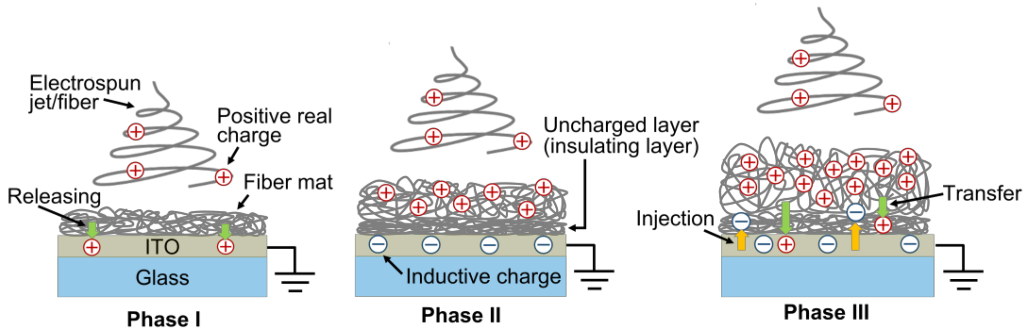
| VES [kV] | Phase I | Phase II | Phase III |
|---|---|---|---|
| 7.0 | 0 min < tdep ≤ 0.75 min | 0.75 min < tdep ≤ 2 min | 2 min < tdep |
| 9.0 | 0 min < tdep ≤ 0.5 min | 0.5 min < tdep ≤ 2 min | 2 min < tdep |
| 11.0 | 0 min < tdep < 0.5 min | 0.5 min ≤ tdep ≤ 2 min | 2 min < tdep |
| tdep [min] | Surface Potential after Peeling off [V] | Amount of Charge [nC] | |
|---|---|---|---|
| Forward | Opposite | ||
| 0.75 | 218 ± 84 | 118 ± 52 | 6.4 ± 2.0 |
| 1 | 182 ± 44 | 110 ± 38 | 5.4 ± 0.9 |
| 1.5 | 256 ± 27 | 125 ± 22 | 8.3 ± 2.9 |
| 2 | 464 ± 52 | 401 ± 83 | 15.4 ± 1.2 |
| 3 | 599 ± 105 | −483 ± 46 | 22.6 ± 1.2 |
| 4 | 688 ± 67 | −362 ± 33 | 22.4 ± 1.0 |
| 5 | 684 ± 26 | −220 ± 29 | 19.1 ± 1.0 |
| 6 | 635 ± 92 | −288 ± 48 | 23.6 ± 2.9 |
| 7 | 255 ± 32 | −214 ± 42 | 10.7 ± 1.0 |
| 8 | 218 ± 42 | −202 ± 83 | 13.4 ± 2.0 |
| 10 | 366 ± 82 | −397 ± 85 | 11.2 ± 0.5 |
| 12 | 305 ± 72 | −287 ± 63 | 13.1 ± 2.0 |
| 15 | 503 ± 44 | −423 ± 55 | 9.9 ± 2.0 |
Publisher’s Note: MDPI stays neutral with regard to jurisdictional claims in published maps and institutional affiliations. |
© 2022 by the authors. Licensee MDPI, Basel, Switzerland. This article is an open access article distributed under the terms and conditions of the Creative Commons Attribution (CC BY) license (https://creativecommons.org/licenses/by/4.0/).
Share and Cite
Iumsrivun, C.; Matsuda, K.; Ohkubo, S.; Ishii, Y. Variable Direct Electromechanical Properties of As-Electrospun Polystyrene Microfiber Mats with Different Electrospinning Conditions. Polymers 2022, 14, 1840. https://doi.org/10.3390/polym14091840
Iumsrivun C, Matsuda K, Ohkubo S, Ishii Y. Variable Direct Electromechanical Properties of As-Electrospun Polystyrene Microfiber Mats with Different Electrospinning Conditions. Polymers. 2022; 14(9):1840. https://doi.org/10.3390/polym14091840
Chicago/Turabian StyleIumsrivun, Chonthicha, Kazuki Matsuda, Shunsaku Ohkubo, and Yuya Ishii. 2022. "Variable Direct Electromechanical Properties of As-Electrospun Polystyrene Microfiber Mats with Different Electrospinning Conditions" Polymers 14, no. 9: 1840. https://doi.org/10.3390/polym14091840