1. Introduction
Nitrogen dioxide (NO
2) is a toxic volatile organic compound that originates from industrial sources such as automobiles. Therefore, it is essential to monitor NO
2 concentrations down to the part-per-billion (ppb) level. While several NO
2-sensing techniques, such as combustion-type sensors, are available, there is a need for instant detection methods like amperometric sensing. Metal oxide-based gas sensors offer precise sensing platforms, but they require high operating temperatures [
1]. In this regard, the development of a room temperature NO
2 sensor compatible with a plastic substrate is necessary. We have previously identified that a polymer semiconductor can serve as an alternative gas-sensing element for a room-temperature-operating NO
2 gas sensor [
2,
3,
4]. This approach offers advantages such as low processing temperature and low production cost [
5]. It is worth noting that polymer semiconductors can be easily deposited using solution processing techniques such as spin-coating, inkjet printing, and roll-to-roll printing [
6,
7].
Since the conductivity of polymer semiconductors is typically low, it is necessary to amplify the charge carrier density of the polymer semiconductor. Therefore, the structure of an organic field-effect transistor (OFET), including the semiconductor, dielectric, and source/drain/gate electrodes, is preferred. With this FET structure, the application of a gate bias can enhance the source–drain current through the field-effect phenomenon [
8,
9]. Gas sensors based on OFETs require several key performance parameters; namely, sensitivity, selectivity, and stability [
10]. Specifically, sensitivity is strongly influenced by OFET characteristics such as field-effect mobility and subthreshold voltage. As gas molecule detection relies on the modulation of the source–drain current in the active channel region, high field-effect mobility facilitates the fast detection of target gas molecules. Extensive research has shown that both the microstructure and molecular structure of the polymer semiconductor affect the performance of OFETs [
11]. Additionally, a few studies have explored the structure–property relationship in OFET-based gas sensors. Our group recently demonstrated that the presence of a glycol side chain in a diketopyrrolopyrrole-based polymer offers advantages for selective NO
2 detection below the ppb level [
12,
13]. Although the glycol side chain degrades the field-effect mobility, it enables efficient gas diffusion for gas absorption and desorption. Consequently, the NO
2-gas-sensing performance is inversely proportional to the crystallinity of the polymer semiconductor used. It is important to note that the simple logic of increasing crystallinity for high-performance OFETs does not apply to OFET-based gas sensors.
From the literature, it has been found that the amorphous polymer poly(triarylamine) (PTAA) can serve as an excellent active layer for OFET-based NO
2 sensors [
14,
15]. PTAA possesses the highest occupied molecular orbital (HOMO) level of −5.14 eV [
16], enabling stable operation in ambient conditions. Although the field-effect mobility of PTAA FETs is approximately 10
−5 cm
2/Vs, PTAA sensors have demonstrated the ability to detect NO
2 concentrations as low as 10 ppb [
15]. In PTAA FETs, the PTAA film functions as the active sensing layer, while the source, drain, and gate electrodes are employed for electrical measurements. By adjusting the gate voltage, the current flow through the PTAA film can be controlled, allowing for the measurement of the response to NO
2 exposure. The mechanism of NO
2 sensing relies on the adsorption of NO
2 on the PTAA surface, which induces changes in the electrical properties of the PTAA FETs. This modulation is typically observed as variations in the charge carrier density and field-effect mobility. However, the precise mechanism of gas detection requires further study, including investigations into gas dynamics (such as diffusion) and device physics. Continued research efforts are aimed at optimizing PTAA-based sensors, which involve the development of novel device structures, surface functionalization techniques, and integration with other materials or technologies to enhance overall sensor performance [
11,
14,
17,
18].
In this report, we investigated the NO2-sensing performance of PTAA FETs with varying device structures; namely, top-contact and bottom-contact, as well as different thicknesses of the PTAA active layer. This study marks the first attempt to compare the gas-sensing properties of bottom-contact FET sensors with the top-contact structure. We used a common SiO2 gate dielectric because of the ease in surface functionalization with a silane coupling agent. Additionally, we examined the impact of surface treatment on the SiO2 dielectric layer and its influence on FET performance. Surface treatment plays a crucial role in enhancing the device performance of PTAA FETs and also affects their gas-sensing properties. Note that charge carrier transport occurs mainly at the interface between the semiconductor and dielectric layer. We analyzed the NO2-sensing performance by evaluating response and recovery rates. Furthermore, we compared the measurement of transfer characteristics before and after NO2 injection. Finally, we proposed a mechanism for gas sensing that takes into consideration different device architectures and surface treatments; this is a novel aspect not previously explored in existing reports.
3. Results and Discussion
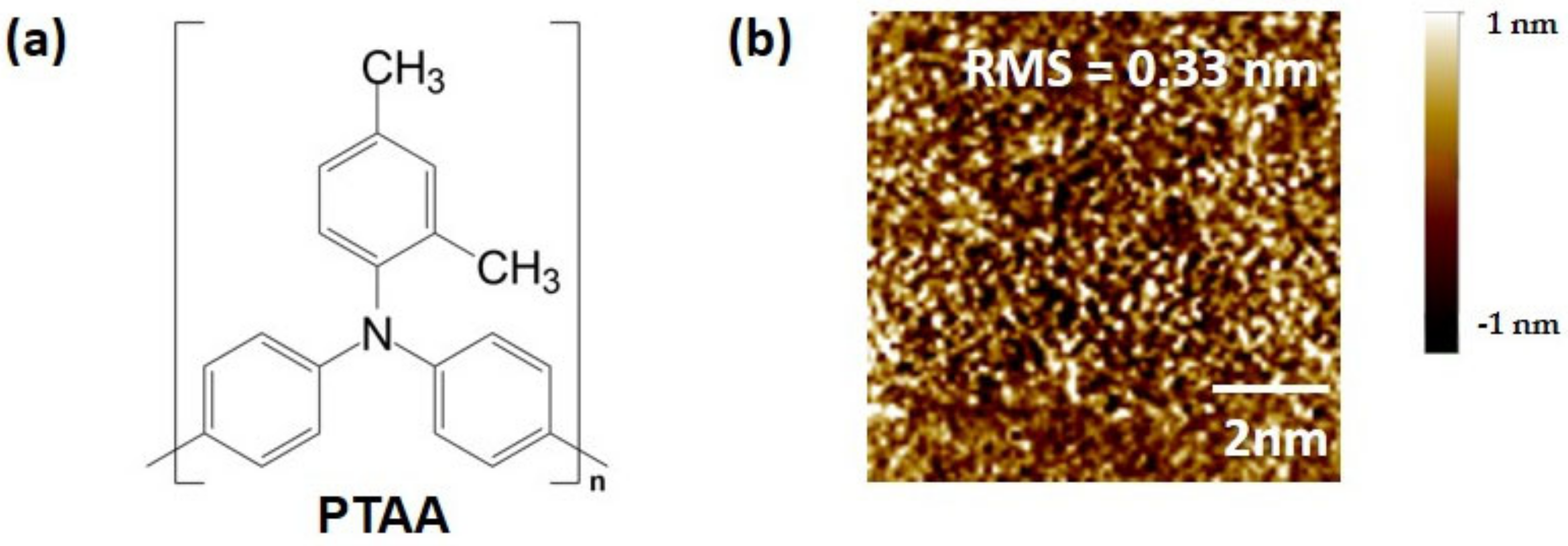
Figure 1a presents the chemical structure of PTAA. In contrast to semicrystalline conjugated polymers like poly(3-hexylthiophene), PTAA incorporates two methyl groups into the aromatic phenyl group. These short aliphatic side chains do not contribute to structural ordering. An AFM image of the PTAA thin-film obtained after spin-casting the PTAA solution is shown in
Figure 1b. The image displays a featureless morphology, and the Root Mean Square (RMS) roughness of the PTAA thin-film was measured to be 0.33 nm. These characteristics provide evidence for the amorphous nature of the PTAA thin-film.
Figure 2 shows the fabrication steps for gas sensors based on top-contact versus bottom-contact FETs. Detailed fabrication steps are illustrated in the Materials and Methods section. As shown in
Figure 3, we fabricated PTAA FETs with different device architectures, while highly doped Si and SiO
2 (thickness of 300 nm) layers serve as the gate electrode and gate dielectric, respectively. The pathways for charge carriers are indicated by the yellow arrows. In the top-contact structure, injected charge carriers move toward the semiconductor–dielectric interface, and adsorption of the target gas can affect both the carrier injection and carrier transport [
19]. In the bottom-contact structure, charge injection mainly occurs at the edge of the source/drain electrodes. Although the area of adsorption in the bottom-contact structure is larger than that in the top-contact structure, the effect of charge injection after gas adsorption is limited, possibly due to the shorter injection path.
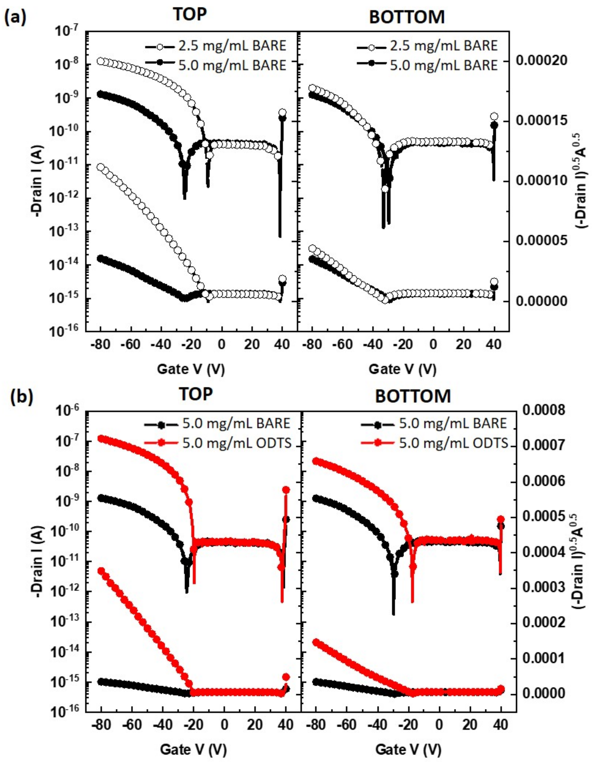
In
Figure 4a, the transfer characteristics of bottom-gate OFETs based on different concentrations of PTAA and device structures are presented. The corresponding device parameters extracted from these transfer characteristics are summarized in
Table 1. The term “Top” represents the top-contact structure, while the term “Bottom” represents the bottom-contact structure of the PTAA FETs. The term “Bare” represents the SiO
2 dielectric without modification, while the term “ODTS” represents the SiO
2 dielectric with ODTS SAMs. For the top-contact structure, an increase in PTAA concentration from 2.5 mg/mL to 5.0 mg/mL (thickness from 18.7 nm to 38.7 nm) resulted in a decrease in both the on-current and threshold voltage, while the off-current remained unchanged. In this structure, the field-effect charge carriers injected from the source electrode are expected to move towards the active channel region near the gate–dielectric layer and subsequently reach the drain electrode, as shown in
Figure 3a. To ensure a shorter injection pathway, a thin semiconducting layer is preferred. It was observed that the field-effect mobility degraded five times when the concentration was doubled (from 2.5 mg/mL to 5.0 mg/mL). On the other hand, in the bottom-contact structure, the on-current and field-effect mobility remained unchanged with varying concentrations. The pathway for charge transport did not significantly change with an increase in the semiconducting layer, as depicted in
Figure 3b. It is important to note that field-effect charge carriers are mostly located in the active channel region near the gate–dielectric layer and the source–drain electrodes [
20]. Therefore, the thick overlayer of amorphous PTAA film in the bottom-contact structure does not play a significant role in the current modulation.
The surface treatment of the gate–dielectric is crucial in controlling the trap density at the interface between the active channel and the gate–dielectric [
20,
21]. Previous studies have reported that hydrophobic self-assembled monolayers (SAMs) can protect silanol groups in SiO
2/Si interfaces [
22]. In
Figure 4b, the transfer characteristics of bottom-gate OFETs based on PTAA with different surface treatments and device structures are depicted. A PTAA concentration of 5.0 mg/mL was used because using 2.5 mg/mL resulted in thin-film dewetting on hydrophobic ODTS SAMs. The surface treatment of the SiO
2 with ODTS SAMs improved the on-current and field-effect mobility, irrespective of the device geometry (top-contact or bottom-contact). The significant increases in field-effect mobility can be directly attributed to the coverage of silanol groups with hydrophobic ODTS SAMs [
23,
24]. Treatment of the SiO
2 surface with ODTS SAMs reduces the number of silanol groups, thereby decreasing the trapping of hole carriers. As PTAA is an amorphous polymer semiconductor, the structural effect of PTAA due to surface treatment is minimal compared to the dominant trap-covering effect. Additionally, the subthreshold slope, which indicates the switching capability, is an important factor. After ODTS surface treatment, the subthreshold slope decreases significantly, indicating an improved switching performance. Simple surface treatment with ODTS SAMs proved advantageous for enhancing the device’s performance in both top-contact and bottom-contact PTAA FETs. Specifically, top-contact FETs based on PTAA thin-films prepared from 5.0 mg/mL and featuring an ODTS interfacial layer represent the optimal conditions for achieving the best switching performance.
To measure the gas-sensing response of the PTAA FETs, NO
2 gas was periodically injected into the gas chamber, which was connected to the current monitoring setup. Since NO
2 is an oxidizing gas and PTAA is a p-type semiconductor, the adsorption of NO
2 to PTAA results in an increase in the accumulation of hole carriers.
Figure 5 illustrates the gas-sensing characteristics of the PTAA FETs based on different concentrations of PTAA and device structures after exposure to 50 ppm NO
2. From these curves, the response rate and recovery rate were extracted and are presented in
Table 2. The response rate is highly dependent on the sensor type, while the recovery rate remains nearly the same regardless of the sensor type. During the 50 s injection of NO
2 (indicated in the grey region), the current in the PTAA FETs increases abruptly, while the current recovers to its initial state during the 1000 s N
2 purging. The sluggish recovery observed after the initial fast recovery may be attributed to the interaction between PTAA and NO
2 [
12]. To enhance the recovery behavior, thermal annealing can be applied. In the top-contact structure, a decrease in the PTAA concentration (from 5.0 mg/mL to 2.5 mg/mL) results in an increase in the response. The electrical properties of the PTAA FETs, such as field-effect mobility and subthreshold slope, are superior in the 2.5 mg/mL device. The fast-switching speed in this device is advantageous for the rapid detection of target NO
2 molecules. In the bottom-contact structure, on the other hand, the change in current upon NO
2 exposure is not significantly affected by the thickness of the PTAA film, which corresponds to the concentration of the PTAA solution. This finding suggests that the adsorption and diffusion of NO
2 onto the PTAA film plays a crucial role in modulating the current in top-contact FETs.
To evaluate the impact of surface treatment and device structure, the NO
2-sensing performance was compared in
Figure 6. The surface treatment of SiO
2 with hydrophobic ODTS SAMs improved the gas response in both the top-contact and bottom-contact devices, which correlates with the enhanced device performance observed in the FETs (as shown in
Table 1). Because the adsorption of NO
2 occurs at the PTAA surface, the hydrophobic character of ODTS did not decrease the gas adsorption and diffusion behaviors. In particular, the top-contact PTAA FETs with ODTS SAMs exhibited an exceptionally high response (>200%/ppm) towards NO
2. This outcome suggests that amorphous PTAA film is well-suited for detecting NO
2 at levels as low as parts per million (ppm).
Several reasons can be proposed to explain the excellent NO
2-sensing performance in top-contact PTAA FETs. Firstly, gas diffusion is facilitated within the amorphous PTAA film. It is speculated that partially positive NO
2 molecules can migrate towards the semiconductor–dielectric interface, particularly at the interface between PTAA and SiO
2. This migration is driven by the electric field generated by the gate bias, and it is applicable regardless of the device structure, whether it is top-contact or bottom-contact. Secondly, the presence of NO
2 molecules within the PTAA film can induce the generation of additional hole carriers, enhancing charge injection along the electrode-active channel pathway. It is worth noting that the HOMO level of PTAA has been reported to be approximately −5.14 eV [
16]. This HOMO level creates a barrier relative to the Fermi level of the Au electrode. It has been observed that evaporated Au electrodes typically have a work function of approximately 4.8 eV [
25,
26]. Due to the generation of hole carriers from the NO
2 molecules, the Fermi level of PTAA could shift upward, facilitating charge injection (
Figure 3c). Indeed, it is noticeable that the top-contact structure has a longer injection path, which can contribute to the enhanced sensing performance in this configuration. On the other hand, in the bottom-contact structure, the injection pathway is short and is weakly affected by the charge carriers generated from the adsorbed NO
2 molecules. As a result, the response in the bottom-contact structure tends to be lower compared to the response observed in the top-contact structure. This is because the distance and pathway for charge carriers to reach the active channel are less favorable for sensing NO
2 gas in the bottom-contact structure.
To further understand the gas-sensing mechanism, transfer characteristics before and after gas injection were compared in
Figure 7. All the curves exhibited significant increases in on-currents, while the off-currents remained unchanged. The minor shift in threshold voltage may be attributed to the combined effects of the NO
2-induced generation of hole carriers and gate bias instability resulting from hole trapping. Notably, there was a substantial increase in field-effect mobility after gas injection, which is calculated and summarized in
Table 3. The increase in field-effect mobility can be attributed to the trap-filling effect in the PTAA film. As mentioned earlier, NO
2 molecules induce the generation of extra hole carriers. These hole carriers fill the trap sites within the PTAA film, leading to an enhancement in the field-effect mobility. It was observed that thicker PTAA films exhibited a higher rate of increase in field-effect mobility, suggesting a higher amount of adsorbed NO
2 molecules in thicker films. However, in the top-contact structure, the increase in mobility (from 3.28 × 10
−5 cm
2/(V·s) to 21.0 × 10
−5 cm
2/(V·s)) was greater in a thinner PTAA film (2.5 mg/mL Top Bare) compared to in a thicker PTAA film (5.0 mg/mL Top Bare), which exhibited an increase from 0.603 × 10
−5 cm
2/(V·s) to 6.65 × 10
−5 cm
2/(V·s). This higher increase in mobility in the thin PTAA film correlates with the higher gas response observed in the 2.5 mg/mL device. In contrast, the bottom-contact structure exhibited a lower increase in mobility and a relatively weaker thickness effect compared to the top-contact structure. This finding supports the assumption that the distance and pathway for charge carriers to reach the active channel play a critical role in the gas response. The top-contact structure with ODTS SAMs exhibited the highest increase in mobility, further supporting the significant effect of surface treatment. It can be proposed that the trap-filling effect is more dominant in the top-contact structure; therefore, top-contact PTAA FETs with ODTS SAMs demonstrate the best sensing performance.


