Low Power SAR ADC Design with Digital Background Calibration Algorithm

Abstract
:1. Introduction
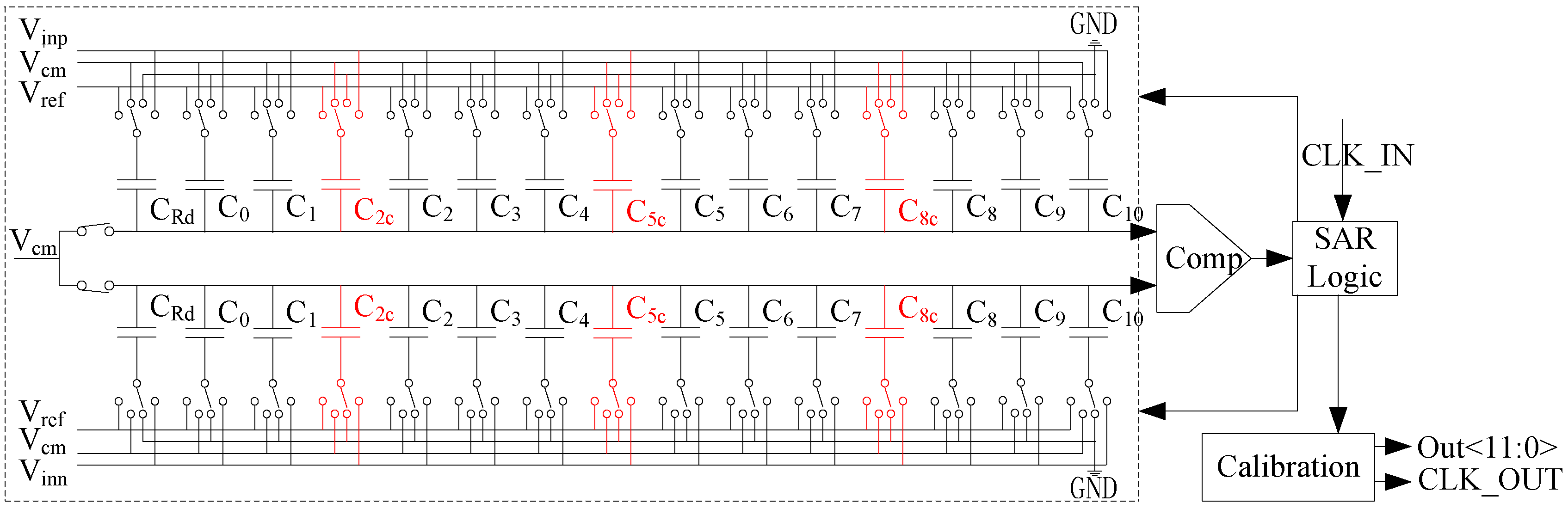
2. ADC Architecture
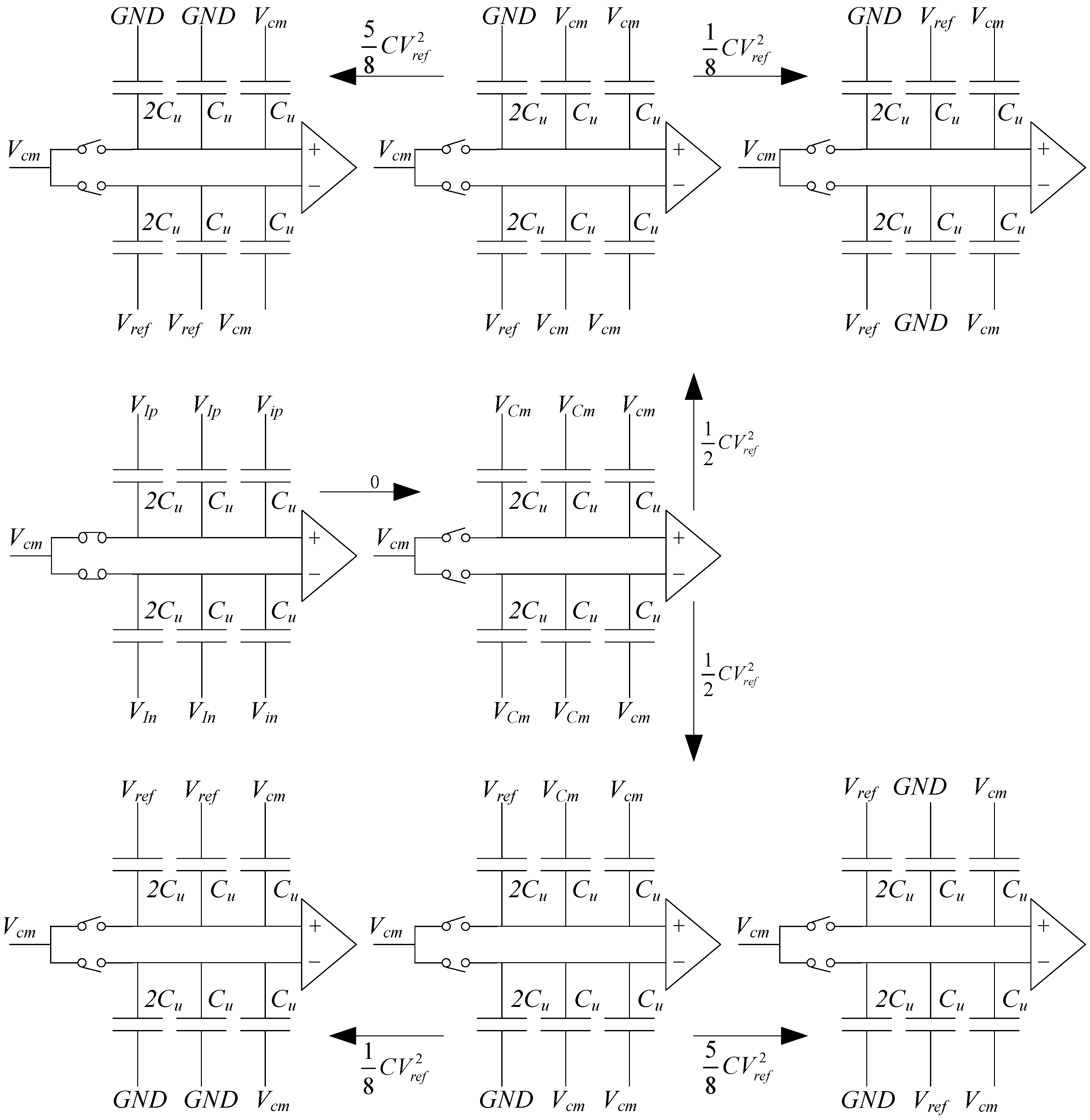
2.1. Switching Method
2.2. SAR Control Logic
3. Calibration Implementation
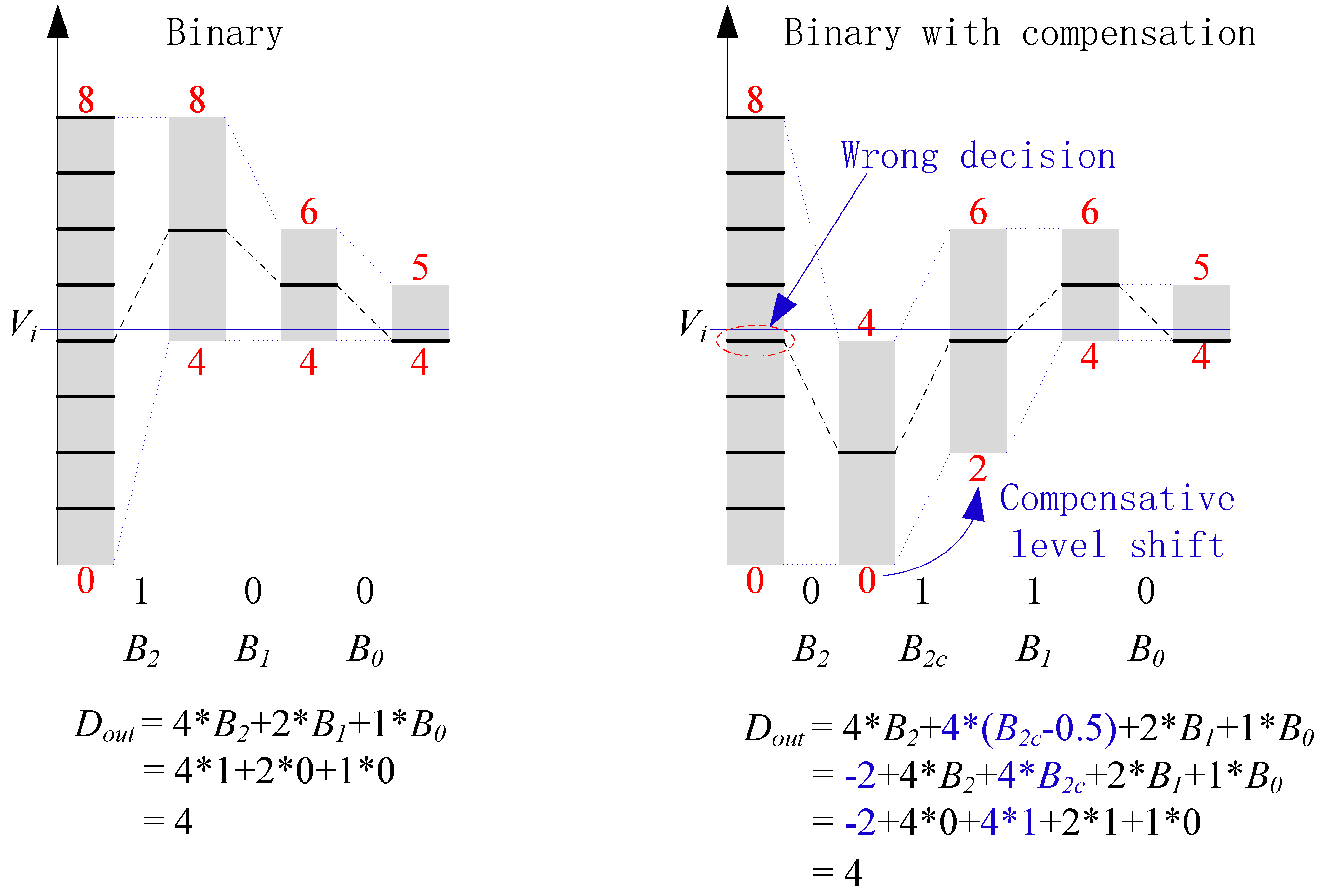
3.1. Capacitor Mismatch
3.2. Calibration Theory
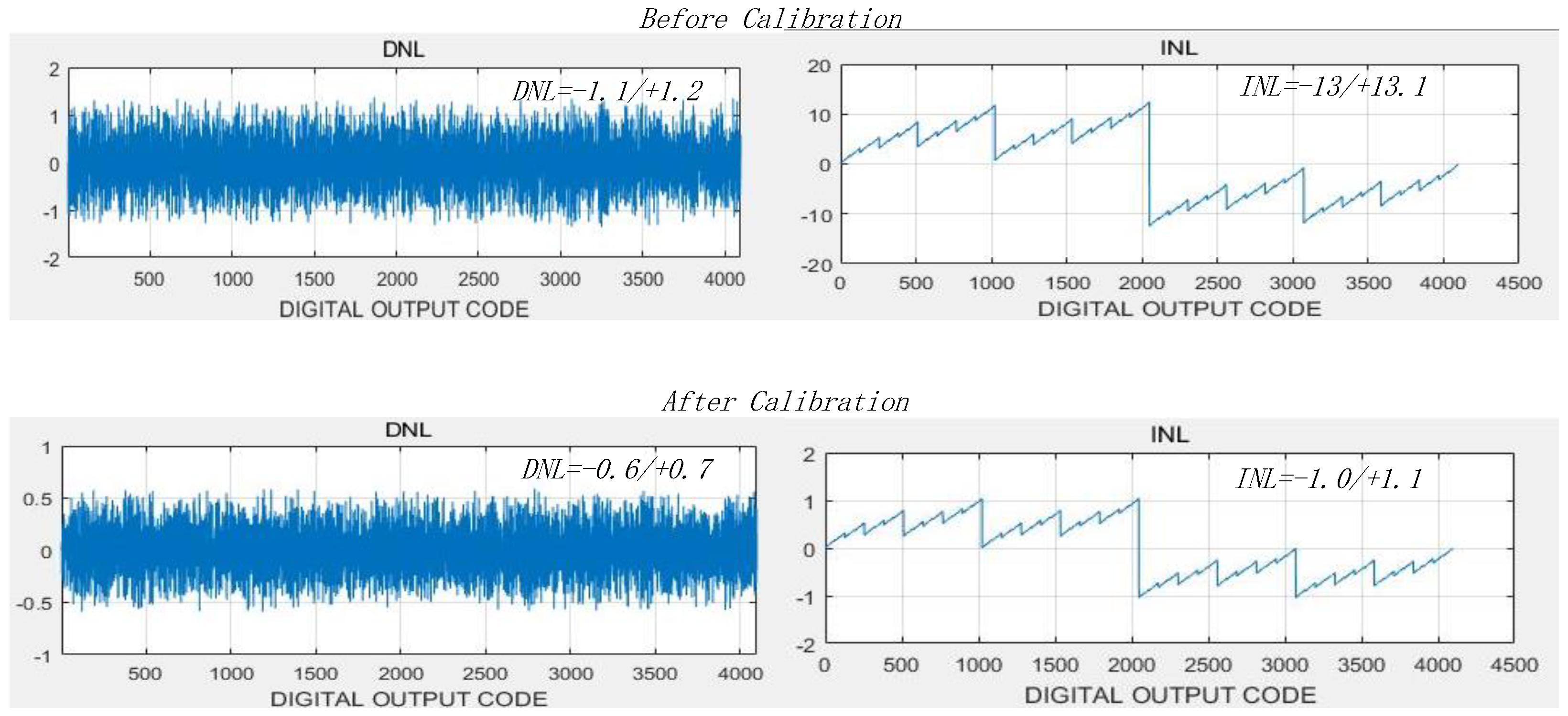
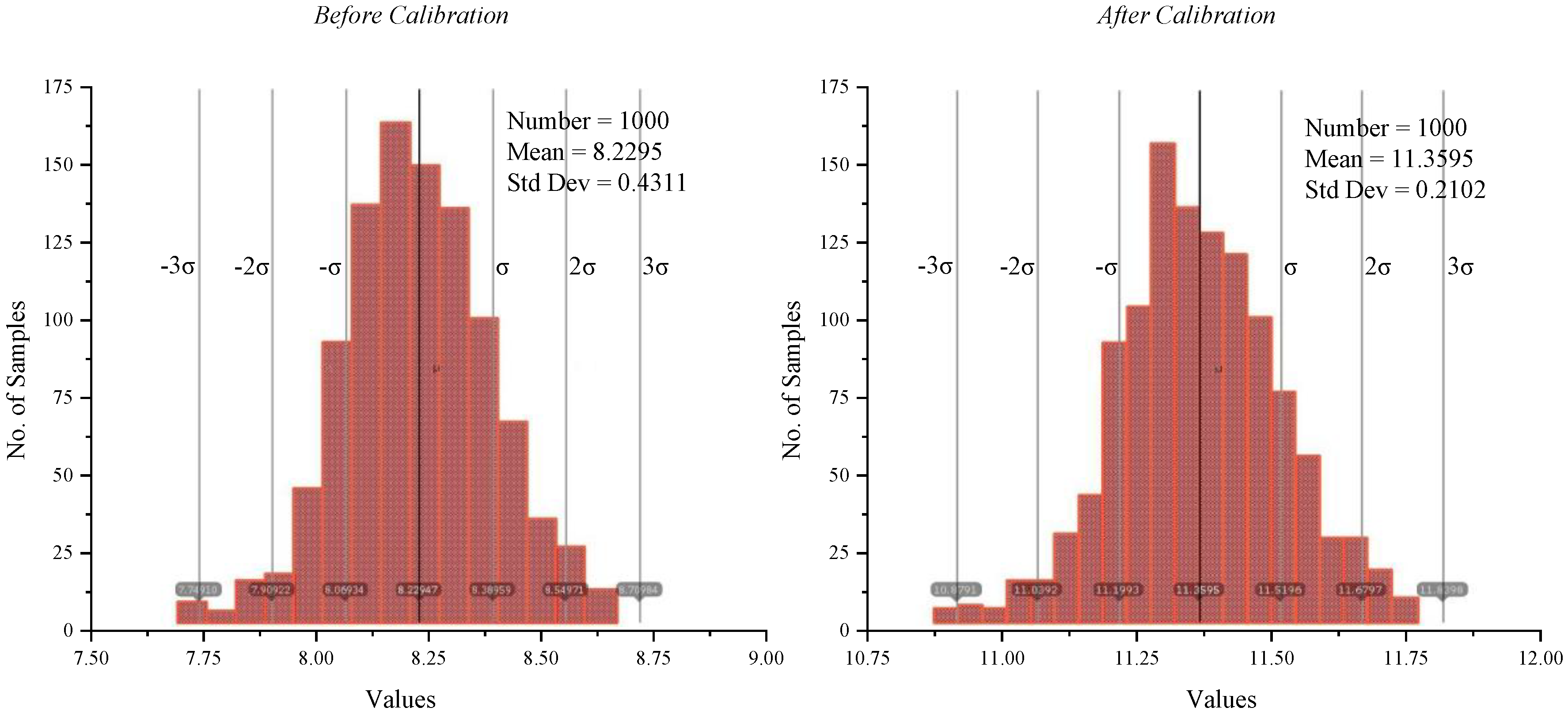
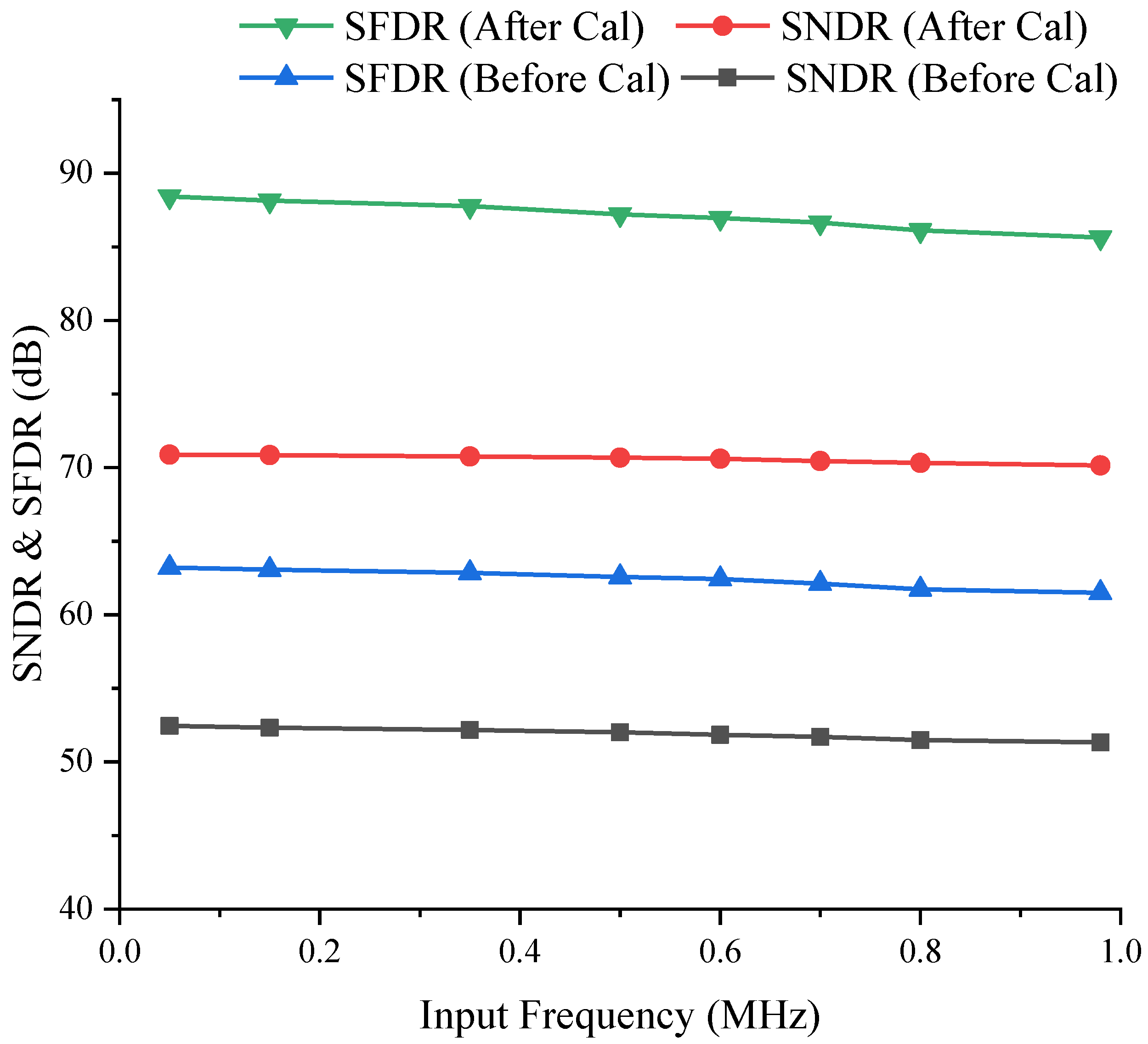
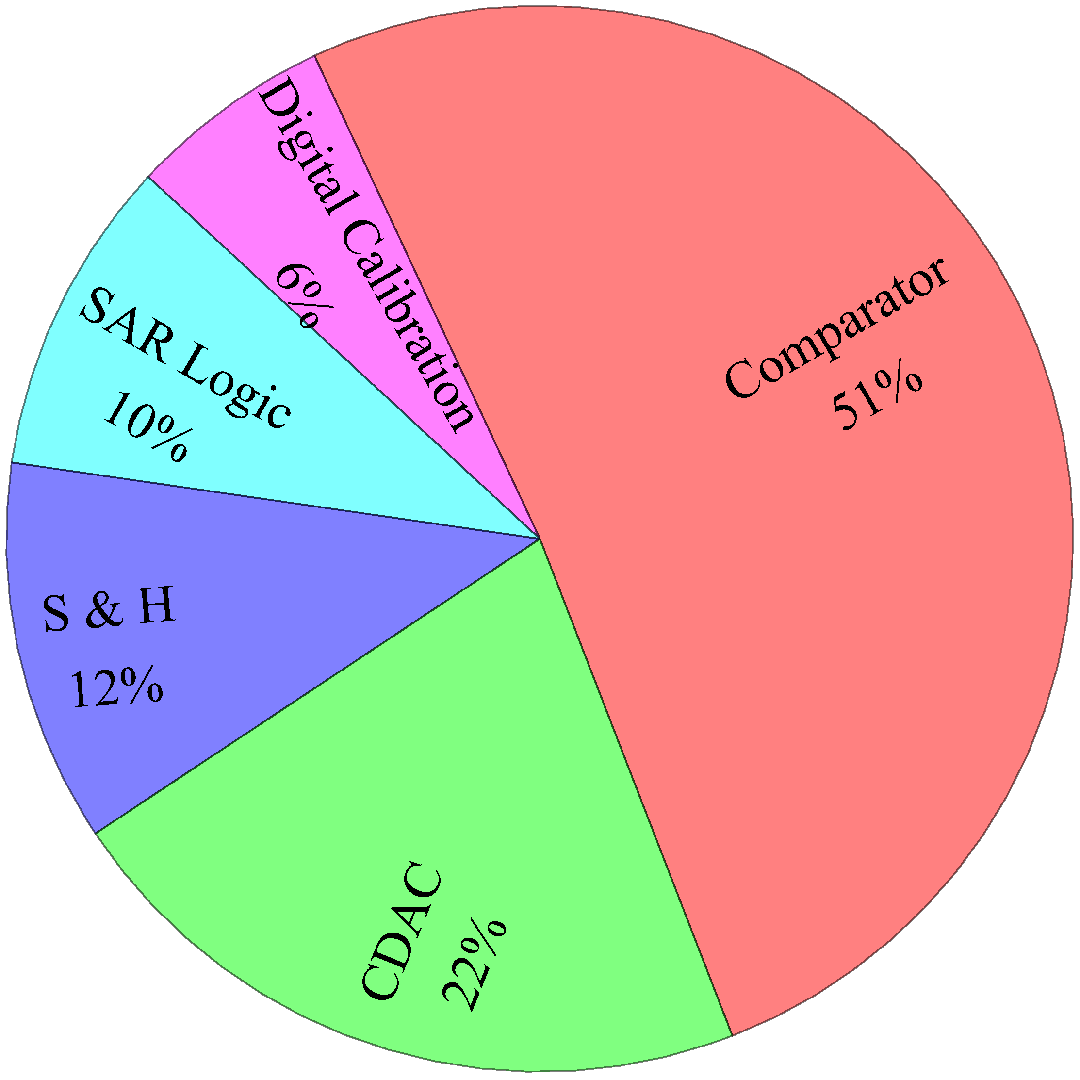
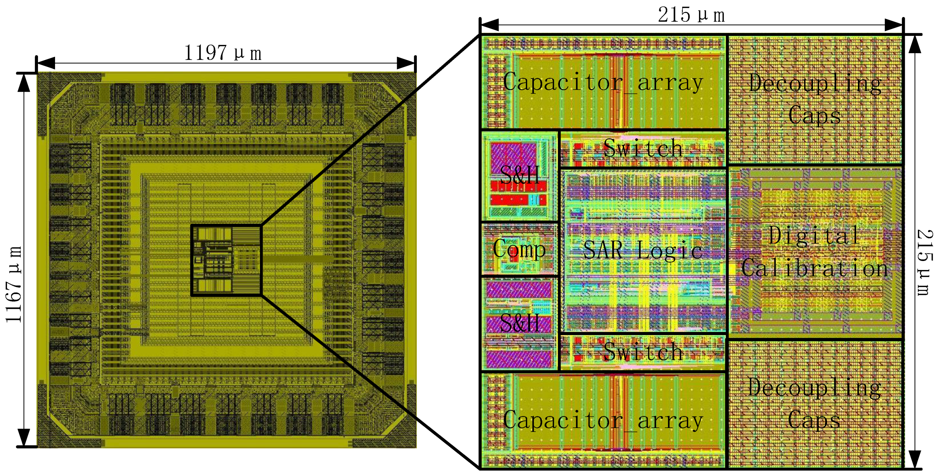
4. Simulation Results
5. Conclusions
Author Contributions
Funding
Acknowledgments
Conflicts of Interest
References
- Liu, W.; Huang, P.; Chiu, Y. A 12b 22.5/45MS/s 3.0 mW 0.059 mm2 CMOS SAR ADC Achieving over 90dB SFDR. In Proceedings of the 2010 IEEE International Solid-State Circuits Conference—(ISSCC), San Francisco, CA, USA, 7–11 February 2010; pp. 380–381. [Google Scholar]
- Berens, M.; Mai, K.; Feddeler, J.; Pietri, S. A General Purpose 1.8-V 12-b 4-MS/s Fully Differential SAR ADC With 7.2-Vpp Input Range in 28-nm FDSOI. IEEE Trans. Circuits Syst. II Express Briefs 2019, 66, 1785–1789. [Google Scholar] [CrossRef]
- Hsu, C.; Chang, S.-J.; Huang, C.-P.; Chang, L.-J.; Shyu, Y.-T.; Hou, C.-H.; Tseng, H.-A.; Kung, C.-Y.; Hu, H.-J. A 12-b 40-MS/s Calibration-Free SAR ADC. IEEE Trans. Circuits Syst. I Regul. Pap. 2018, 65, 881–890. [Google Scholar] [CrossRef]
- Venca, A.; Ghittori, N.; Bosi, A.; Nani, C. A 0.076 mm2 12 b 26.5 mW 600 MS/s 4-Way Interleaved Subranging SAR-ΔΣ ADC With On-Chip Buffer in 28 nm CMOS. IEEE J. Solid-State Circuits 2016, 51, 2951–2962. [Google Scholar] [CrossRef]
- Zhu, Y.; Chan, C.; Wong, S.; Seng-Pan, U.; Martins, R.P. Histogram-Based Ratio Mismatch Calibration for Bridge-DAC in 12-bit 120 MS/s SAR ADC. IEEE Trans. Large Scale Integr. (VLSI) Syst. 2016, 24, 1203–1207. [Google Scholar] [CrossRef]
- Wang, P.; Sun, J.; Wu, J. Dither-based background calibration of capacitor mismatch and gain error in pipelined noise shaping successive approximation register ADCs. Electron. Lett. 2019, 55, 984–986. [Google Scholar] [CrossRef]
- Matsui, T.; Sento, K.; Ebata, T.; Ishibashi, A. A Capacitor Dielectric Relaxation Effect Cancellation Circuit in a 12-Bit, 1-MSps, 5.0-V SAR ADC on a 28-nm Embedded Flash Memory Microcontroller. IEEE Solid-State Circuits Lett. 2019, 2, 95–98. [Google Scholar] [CrossRef]
- Liu, C.-C.; Huang, M.-C.; Tu, Y.-H. A 12 bit 100 MS/s SAR-Assisted Digital-Slope ADC. IEEE J. Solid-State Circuits 2016, 51, 2941–2950. [Google Scholar] [CrossRef]
- Chung, Y.; Yen, C.; Tsai, P.; Chen, B. A 12-bit 40-MS/s SAR ADC with a Fast-Binary-Window DAC Switching Scheme. IEEE Trans. Large Scale Integr. (VLSI) Syst. 2018, 26, 1989–1998. [Google Scholar] [CrossRef]
- Zhong, J.; Zhu, Y.; Chan, C.; Sin, S.; Seng-Pan, U.; Martins, R.P. A 12b 180MS/s 0.068mm2 With Full-Calibration-Integrated Pipelined-SAR ADC. IEEE Trans. Circuits Syst. I Regul. Pap. 2017, 64, 1684–1695. [Google Scholar] [CrossRef]
- Chung, Y.; Zeng, Q.; Lin, Y. A 12-bit SAR ADC With a DAC-Configurable Window Switching Scheme. IEEE Trans. Circuits Syst. I Regul. Pap. 2020, 67, 358–368. [Google Scholar] [CrossRef]
- Collins, N.; Tamez, A.; Jie, L.; Pernillo, J.; Flynn, M.P. A Mismatch-Immune 12-Bit SAR ADC with Completely Reconfigurable Capacitor DAC. IEEE Trans. Circuits Syst. II Express Briefs 2018, 65, 1589–1593. [Google Scholar] [CrossRef]


| Specifications | Ref. [2] | Ref. [3] | Ref. [4] | This Work |
|---|---|---|---|---|
| Architecture | SAR | SAR | SAR | SAR |
| Technology(nm) | 28 | 40 | 28 | 40 |
| Supply(V) | 1.8 | 1.0 | 1.2/1.5 | 1.2 |
| Sampling Rate(MS/s) | 4 | 40 | 600 | 2 |
| Resolution(bit) | 12 | 12 | 12 | 12 |
| SNDR(dB) | 70.1 | 63.46 | 60.7 | 70.15 |
| SFDR(dB) | 84.3 | 73.72 | — | 85.63 |
| ENOB(bit) | 11.35 | 10.25 | 9.79 | 11.36 |
| DNL(LSB) | +0.2/−0.2 | +0.51/−0.49 | — | +0.7/−0.6 |
| INL(LSB) | +0.6/−0.6 | +1.95/−1.44 | — | +1.1/−1.0 |
| Power(mW) | 1.73 | 1.25 | 26.5 | 0.3564 |
| FOM(fJ/conv.-step) | 165.5 | 25.7 | 68 | 67.80 |
| Active Area(mm2) | 0.13 | 0.04 | 0.076 | 0.046 |
Publisher’s Note: MDPI stays neutral with regard to jurisdictional claims in published maps and institutional affiliations. |
© 2020 by the authors. Licensee MDPI, Basel, Switzerland. This article is an open access article distributed under the terms and conditions of the Creative Commons Attribution (CC BY) license (http://creativecommons.org/licenses/by/4.0/).
Share and Cite
Li, S.; Chen, J.; Liang, B.; Guo, Y. Low Power SAR ADC Design with Digital Background Calibration Algorithm. Symmetry 2020, 12, 1757. https://doi.org/10.3390/sym12111757
Li S, Chen J, Liang B, Guo Y. Low Power SAR ADC Design with Digital Background Calibration Algorithm. Symmetry. 2020; 12(11):1757. https://doi.org/10.3390/sym12111757
Chicago/Turabian StyleLi, Shouping, Jianjun Chen, Bin Liang, and Yang Guo. 2020. "Low Power SAR ADC Design with Digital Background Calibration Algorithm" Symmetry 12, no. 11: 1757. https://doi.org/10.3390/sym12111757
APA StyleLi, S., Chen, J., Liang, B., & Guo, Y. (2020). Low Power SAR ADC Design with Digital Background Calibration Algorithm. Symmetry, 12(11), 1757. https://doi.org/10.3390/sym12111757