1. Introduction
SSDs with flash memory as the storage medium are replacing HHD as the main storage device. Compared with HDD, SSD has fast read and write speed, good shock resistance and low power consumption [
1]. At the same time, with the improvement of flash memory manufacturing technology, the capacity of flash memory is rapidly increasing, and the capacity of a single SSD has been further improved.
Flash memory can be divided into four levels: target, logical unit (LUN), block, and page [
2]. A block consists of multiple pages. A block is the basic unit of data erasure, and a page is the basic unit of read and write operations in flash memory [
3]. When data are updated on a page, the block where the page is located must be erased before data can be updated on the page. In order to improve performance, SSD generally adopts an offsite update method. When the data of a certain page need to be updated, the SSD writes the new data to a new page first and marks the original page as invalid. However, as the SSD usage time increases, the number of invalid pages also increases. In order to reuse these invalid pages, the SSD will recycle them and reallocate those [
4]. The reclamation process consumes a lot of system overhead, which causes the SSD performance to decrease. At the same time, since the number of program/erasures (P/E) cycles of the blocks in the SSD is limited, the number of P/E cycles of the SLC architecture is about 100K, the number of P/E cycles of the MLC is about 10K, and the number of P/E cycles of the TLC is about 1K [
5]. The latest QLC P/E cycles have been reduced to 500 [
6]. As the usage time of an SSD increases, its reliability gradually decreases.
In order to improve the reliability and read/write performance of SSDs, researchers have carried out a lot of research work and obtained a lot of research results. These research results include wear-leveling technology, bad block management methods and on-chip Raid. Through the application of these results, the reliability and service life of the SSD are greatly improved. For example, wear-leveling can evenly spread the wear of NAND Flash in each block—thus reducing the failure of a block in NAND Flash due to excessive wear [
7]. However, these research results have not fundamentally reduced SSD user data writing. The main methods to improve SSD performance include: I/O performance optimization, garbage collection method optimization, and address mapping table scheduling optimization [
8]. For example, Huyang [
9] proposed an SSD multi-level parallel optimization method. This method optimizes the internal channel, chip, target, and LUN of the SSD in parallel, thereby improving the performance of the SSD. At present, there are two main methods for reducing data writing: data deduplication and data compression. Data deduplication is mainly to eliminate redundant data in the written data, thereby reducing data writing. Data compression is to compress the written data, thereby reducing data writing.
According to the compression model, compression algorithms can be divided into two types: lossless compression and lossy compression. Compared to lossy compression, the compression ratio of lossless compression is not high, but it completely saves the original information without any data loss, and gradually alleviates the disadvantages of lossless compression, which makes the lossless compression format have broad application prospects [
10]. As a data storage medium, the SSD must guarantee the absolute integrity of the stored data. Therefore, this paper conducts research and optimization based on the uncompressed algorithm.
Lossless compression technology is to achieve the purpose of compressing data by encoding a large amount of data on the premise that data cannot be lost. The compressed data can be restored to the original data state by decompression. Lossless compression can be divided into statistical model based compression [
11] and dictionary based compression [
12].
The dictionary based compression has two advantages. First, the algorithm only includes string-based search and matching, and there is no calculation processing on numerical values. Second, the algorithm is very simple and fast in the decompression process. In statistical model based compression, its decompression is usually as complex as the inverse process of compression. Abraham Lempel and Jacob Ziv proposed the LZ77 algorithm jointly. This compression algorithm is based on a dictionary model, using a dictionary to encode each string into an identifier. When the string appears again in the compressed data, the identifier is used to replace the string to achieve the purpose of compression [
13]. Benini et al. investigated a hardware-assisted data compression method for memory. This method is similar to the LZ algorithm. They describe in detail how the method is implemented in hardware and use this method for data compression with almost no performance loss [
14]. Kjelso et al. proposed the X-Match compression algorithm for main memory, which is easy to implement in hardware. X-Match is another variant of LZ77, differing in that phrases matching works in four byte units [
15]. The LZW algorithm is an optimization algorithm based on the LZ78 algorithm proposed by Welch. The algorithm has good compression performance, fast speed, and easy implementation, and it is one of the most commonly used and most effective lossless compression methods. The LZW algorithm completes the conversion from input to output by managing a dictionary. The LZW compression algorithm uses a greedy analysis method. Each analysis always serially checks the data in the forward buffer, analyzes the longest string appearing in the current dictionary, outputs its corresponding code, and then adds the next input character after the string forms a new string and is added to the dictionary [
16]. Compared with other algorithms optimized on the FPGA platform, the performance of the LZW algorithm is much better [
17].
Therefore, this article mainly discusses data compression technology. Based on the improvement of the existing LZW data compression algorithm, a data compression method is designed in accordance with the characteristics of SSD. This method can reduce the P/E cycle of the SSD. At the same time, this study is optimized for Flash Translation Layer (FTL) to ensure that the performance of SSD is basically not affected after the data compression is introduced.
The rest of the article is organized as follows. The second section describes the principle and implementation of the SSD data compression method based on block division. The third section carried out relevant tests on the method, and obtained the data deduplication efficiency and read/write performance of the method under different workloads. The last section summarizes this article and gives relevant conclusions.
2. Materials and Methods
In order to improve the SSD data compression performance, this study proposes an SSD data compression method based on the zone of flash memory (ZDC). This method is based on the LZW compression algorithm. By optimizing the LZW algorithm and the address mapping table, fast compression of the internal data partition of the SSD is realized.
The data compression method designed in this study has two characteristics. First, this study uses an Intel SoC chip as the controller of the SSD. The chip includes a dual-core ARM CPU and a set of field programmable logic arrays (FPGAs). Second, ZDC is an offline solid state disk data compression method. ZDC will first judge the type of input quantity instead of immediately compressing the input data. If the data is hot and updated frequently, ZDC will not immediately compress the hot data. On the contrary, ZDC will immediately compress cold data with low update frequency.
2.1. System Summary Architecture
This research is mainly to improve the performance and reliability of SSDs by introducing data compression method in the SSD. First, this study divides an SSD into multiple zones according to capacity. Each zone uses page-level address mapping. Second, this study divides the data in each zone into hot data and cold data according to P/E cycles. Third, choose the right time for data compression according to different data types (hot data or cold data). Fourth, this study designed a new garbage collection method. This method can meet the new requirements for garbage collection after data compression.
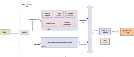
Figure 1 shows the overall structure of the study. This research uses a SoC as the controller of the SSD. The controller mainly includes interface module, CPU module, FPGA module, and NAND Flash controller module.
The Interface module is mainly used for the analysis of interface protocols. After the protocol analysis is completed, the data sent by the host are divided into types. The data of command and address will be sent to the CPU in the controller for further processing. User data is sent to the FPGA for compression.
The CPU in the SoC mainly performs FTL management. Functions in FTL include address mapping, static wear-leveling, garbage collection and bad block management. In addition, since the cache is set outside the SSD controller, the functions of the CPU also include management of the cache. Through the address mapping function in FTL, the zone division of NAND Flash memory space is realized. The specific division is introduced in
Section 2.3.
The FPGA mainly implements data compression. When the host sends a write request, the SSD first transmits the write request information to the FTL. This information includes the write command, the starting logical address, and the file capacity. Then, calculate the physical address through the address mapping table in the FTL. Finally, it is determined whether the data are compressed immediately by judging whether the data corresponding to the physical address is hot or cold.
2.2. Data Compression
In this study, the optimized LZW compression algorithm is used inside the SSD to achieve data compression. Although the original LZW algorithm has high data compression efficiency, it also has certain limitations when it is introduced into the embedded SSD controller. First, the LZW compression algorithm requires a dictionary to record the most recently entered string entries. When new string data arrive, it needs to try to scan the dictionary for the corresponding dictionary entry. Second, when a new string entry is recorded in the dictionary, the entire string is recorded into the dictionary entry. This causes the dictionary to be too large, and the search needs to be repeatedly compared and repeated many times, resulting in time and waste of space. Third, as the compressed data increases, more and more strings are entered into the dictionary. When the dictionary has no capacity to record new entries, the old string is not replaced with a suitable replacement strategy. Generally, the LZW algorithm uses all the dictionary to be cleared, and the method is re-established. This strategy implicitly assumes that new data is more favorable to subsequent characters than old data. Aiming at the limitations of the LZW algorithm, this study optimized the LZW algorithm based on the characteristics of the embedded SSD controller.
First, because the SoC is used as the SSD controller platform in this study, the internal FPGA has good parallel characteristics. Therefore, this study will implement multiple dictionaries inside the FPGA. In data compression, multiple dictionaries work in parallel to match input strings. Finally, the dictionary with the most matches is selected as the output. The parallel compression process of the LZW algorithm is shown in
Figure 2. In this research, eight dictionaries work in parallel in FPGA. At the same time, this study is based on the partitioning of flash memory. The specific partitioning method will be described in
Section 2.3. Each zone will correspond to a set of dictionaries.
Secondly, since the compression method is implemented in an embedded system, and the hardware resources of the embedded system are very limited, a suitable dictionary capacity must be determined. Burrows et al. [
18] and Yim et al. [
19] have shown that there is no significant difference in the compression ratio for 2 KB to 8 KB compression unit sizes. At the same time, the capacity of the storage device increases at any time. At present, the file system is basically 4 KB in block capacity. The read and write requests are based on 4 KB as the basic unit. Most flash memory page sizes are also 4 KB. Therefore, selecting 4 KB for the dictionary capacity can improve SSD performance.
Finally, the storage space of the dictionary is limited. As the compressed data increase, more and more strings are entered into the dictionary. Once the dictionary has no capacity to record new entries, it generally deletes all the contents of the dictionary and re-creates the dictionary. However, SSD is a kind of data storage device and the data stored in SSD has a certain locality in time [
20,
21]. This means that, although the current data may not be matched, after a period of time, new data may be matched. Therefore, the entire contents of the dictionary are deleted, and a new dictionary is rebuilt. This will not only improve the hit rate but also lead to a reduction in the overall SSD performance. This research uses a replacement strategy, which sorts the contents of each dictionary according to the frequency of hit ratio. When there is no hit, the system automatically deletes the dictionary with the lowest hit rate and re-creates an entry. In order to sort the entry hit ratios, this study defines a variable Ki (i = 0 ... 7). Ki indicates the number of times the i-th entry has not been hit. In extreme cases, the K value of one or more terms is out of bounds. When K values are out of bounds, all K values corresponding to all terms are cleared to 0 and re-counted.
2.3. Mapping Table Optimization
Due to the spatial locality of the data, this study did not directly adopt the page-level address mapping method, but divided the SSD storage space into multiple zones, and each zone used page-level address mapping. Each zone that is divided consists of three parts. These three parts store user data, address mapping table and dictionary data, respectively.
Figure 3 is a flash memory array divided into four zones.
Under normal circumstances, only one zone’s address mapping table (ZAM) will be loaded into the cache. The structure of the ZAM is shown in
Table 1.
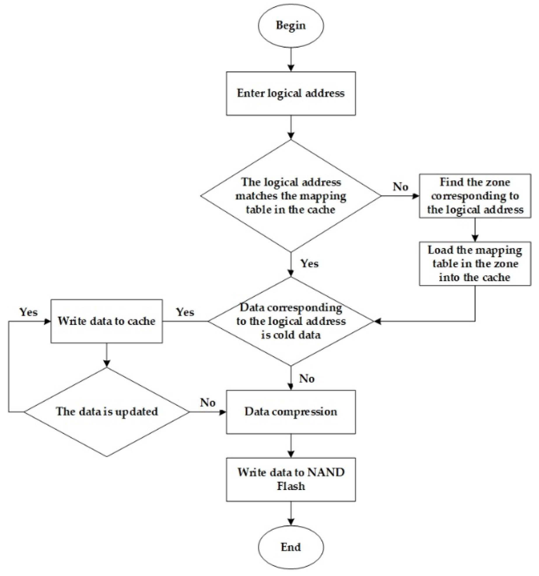
When SSD obtains a write request, SSD controller processes the request as follows. 1. The SSD judges whether the logical address of the write request matches the address mapping table in the cache. 2. If the logical address matches the address mapping table in the cache, the SSD then determines whether the physical address corresponding to the logical address is a hot block according to the value of EraseNB. 3. If the block corresponding to the physical address is a hot block, the SSD caches the written data in the cache and does not compress it. If it is a cold block, the SSD compresses the data and writes it directly to the corresponding physical page. 4. If the cache does not contain the logical address, the SSD searches for the corresponding zone based on the logical address. 5. The SSD loads the address mapping table corresponding to the searched zone into the cache and repeats step 3. The data write process of SSD is shown in
Figure 4.
Due to the limitation of cache capacity, this study only loads the address mapping table of a zone into the cache. When a logical address cannot match the address mapping table in the cache, the SSD needs to search for a zone to which the logical address belongs and load the address mapping table of the zone into the cache. For this research, a zone search directory table (ZDT) is designed. Through this directory, the SSD can search for each logical address corresponding to the zone. The structure of ZDT is shown in
Table 2.
ZNB indicates the number of the zone. For each zone, the number is unique.
SZPAN indicates the starting physical address of each zone. After the SSD receives the logical address sent by the host, it calculates the physical address corresponding to the logical address. SSD judges which zone the logical address belongs to base on the calculated physical address.
ZMatch indicates the number of times each zone was requested to be hit in the cache. The more times a zone is hit, the more easily the data stored in the zone can be updated. When the SSD starts, load the zone corresponding to the maximum ZMatch into the cache.
ZAM_PA represents the physical address of each ZAM stored in NAND Flash. When the SSD needs to load a new ZAM into the cache, the SSD first searches the ZAM’s position in the NAND Flash through ZAM_PA, and then the SSD can read the ZAM into the cache through ZAM and offset.
For example, as shown in
Figure 5, the host sends three write requests. The LPAs for these three write requests are: 0010, 1001, and 0101. After address mapping, the SZPBA corresponding to the three requests are 0000, 100, and 0100. By querying the ZDT, the zones corresponding to the three write requests are zone_0, zone_2, and zone_1. Since the ZMatch value corresponding to zone_1 is the largest, the ZAM corresponding to zone_1 is loaded into the cache and the ZAM corresponding to the remaining zones is stored in the NAND Flash. After determining the specific physical address of each LBA, the process shown in
Figure 4 performs data compression and storage.
2.4. Garbage Collection
In order to reduce the impact on the performance of SSD during garbage collection, based on the zone division method of flash memory space, a local SSD garbage collection method was designed. This method performs garbage collection only on the area of the ZAM table in the cache. When the number of invalid blocks in the ZAM reaches 80% of the total number of blocks in the region, the SSD starts a garbage collection mechanism, modifies the ZAM, and erases the invalid blocks in the region. The area where the ZAM is stored in the NAND Flash is not included in garbage collection. Only when the area ZAM is loaded into the cache will the SSD controller first determine whether the area needs to be included in garbage collection. If garbage collection is required, the data written by the host is cached in the cache first, and, after the garbage collection is completed, compression and writing are performed. If garbage collection is not required, follow the procedure shown in
Figure 5.
Using local garbage collection measurement has the following advantages: 1. Because the local garbage collection is performed, fewer data blocks are erased, which improves the garbage collection efficiency and reduces the impact of garbage collection on the performance of the solid state disk. 2. The amount of data that needs to be moved during garbage collection is smaller than the amount of data moved during full garbage collection, which can also speed up garbage collection efficiency and improve performance.
3. Results and Discussion
Flash-DBSim [
22] is a simulation tool for flash technology research. Flash-DBSim can simulate various experimental environments appearing in flash technology research as accurately as possible. It is a unified flash experiment simulation platform. Flash-DBSim was developed using Microsoft Visual Studio 2008 and uses C ++ language to achieve different levels of solid state disk encapsulation.
Flash-DBSim uses a three-tier structure and each module uses interfaces to interact. The function of each module is divided into VFD module and FTL module.
VFD module: This module is used to simulate the characteristics of NAND/NOR flash devices, such as: data page, block size, number, read and write latency, erase limit, I/O count, and concurrency control of flash devices.
FTL module: This module provides address translation and access interfaces to the underlying flash device. This module can use the FTL/NFTL algorithm to control the underlying module. At the same time, upper-level users can access Flash-DBSim by interacting with this module.
Public access interface: The public access interface is open to users. This interface layer hides all implementation details in the Flash-DBSim system. Users use these interfaces to control the operation of the Flash-DBSim system.
This study uses Flash-DBSim to simulate a 128 GB flash memory. The SSD is divided into four zones. The capacity of each zone is 32 GB. At the same time, the traditional page-level mapping algorithm is implemented in Flash-DBSim, and the same data environment is used for testing.
In order to verify the storage management algorithm designed in this paper and evaluate its performance, this paper implements demand-based mapping algorithm (DFTL) based on Flashsim and the compression mapping algorithm designed in this paper—Run DFTL and this method on the Flash-DBSim simulation tool, respectively. This experiment uses a random write method and the test data is shown in
Table 3.
3.1. Write Amplification
Write amplification is an important indicator for testing SSDs. On the one hand, write amplification cannot be avoided due to the difference between the flash storage media used by SSDs and the storage media of traditional disks. On the other hand, the write amplification can be significantly reduced by optimizing the FTL algorithm. The write amplification largely determines the write speed of the SSD, and, at the same time, it is related to the service life of the SSD. Through the above test results, the write amplification test results can be obtained by simple processing (see
Figure 6).
From, the following conclusions can be drawn. After introducing a data compression method inside the SSD, the write amplification level of the SSD can be significantly reduced. However, when testing the write amplification of compressed files, the compressed file is already compressed on the host side, so the method proposed in this study is the same as that of DFLT when writing amplification of compressed files.
3.2. Read and Write Latency Test
In this test, we will perform DFTL and this study on page read and write performance. The selected test data is shown in
Table 3.
Random read test method: write a page to flash memory every 1 second, which can be any segment of data in any type of file to test burst write delay. The experimental results are the average of the test results on each page.
Random write test method: Read data from any page in flash memory every one second. In order to prevent the effects of caching and other factors, this test reads in the order of LPN increasing by eight pages at a time.
Sequential read and write test method: As long as the flash memory is idle, a read (or write) operation request is issued to the Flash, the address is random, and the amount of data is an indefinite number of pages.
Since the data is already compressed at the time of writing, the data actually written into the flash memory will decrease. SSD performance, especially random read and write performance, has been greatly improved.


