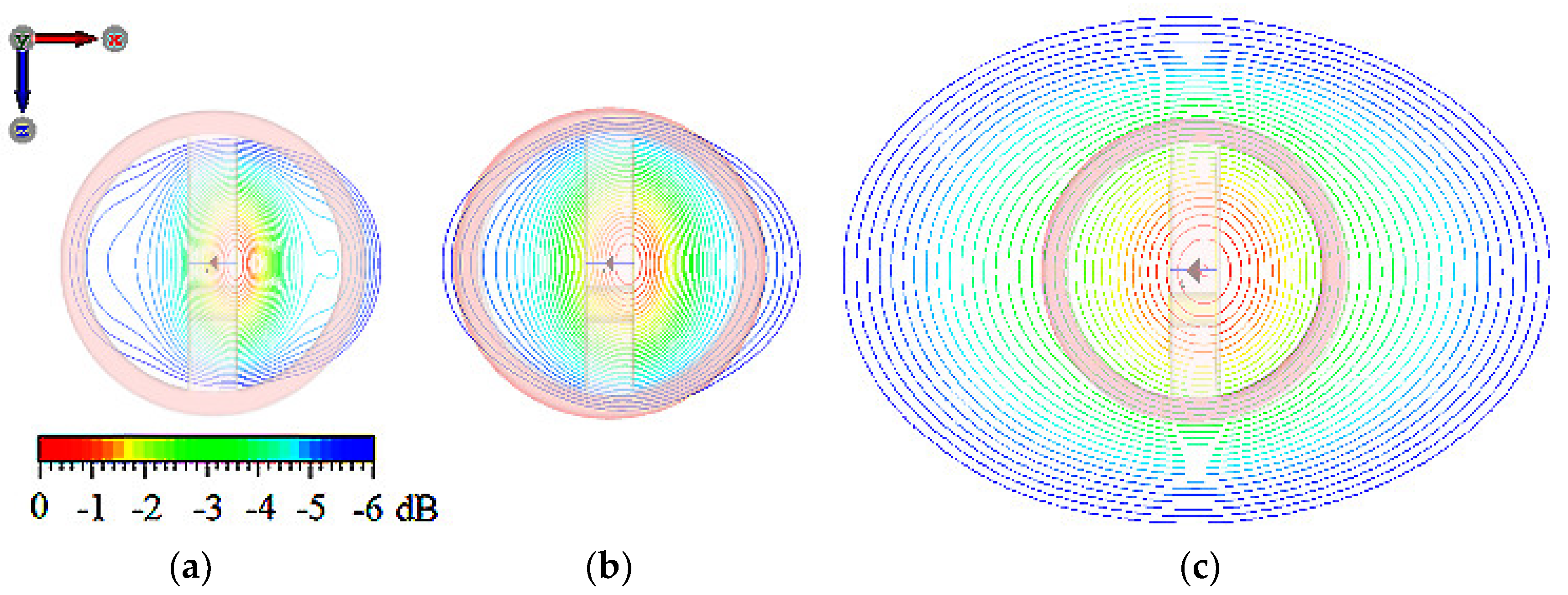
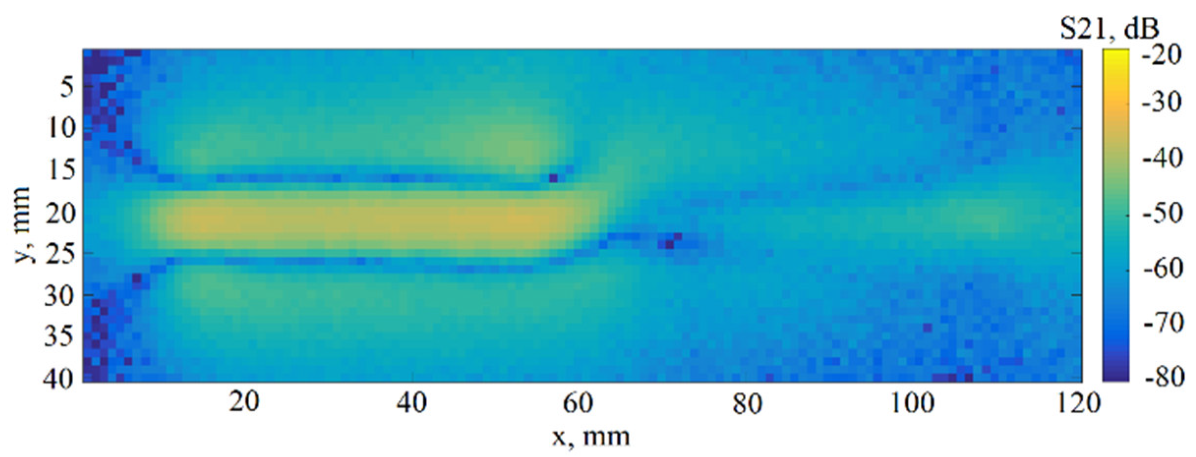
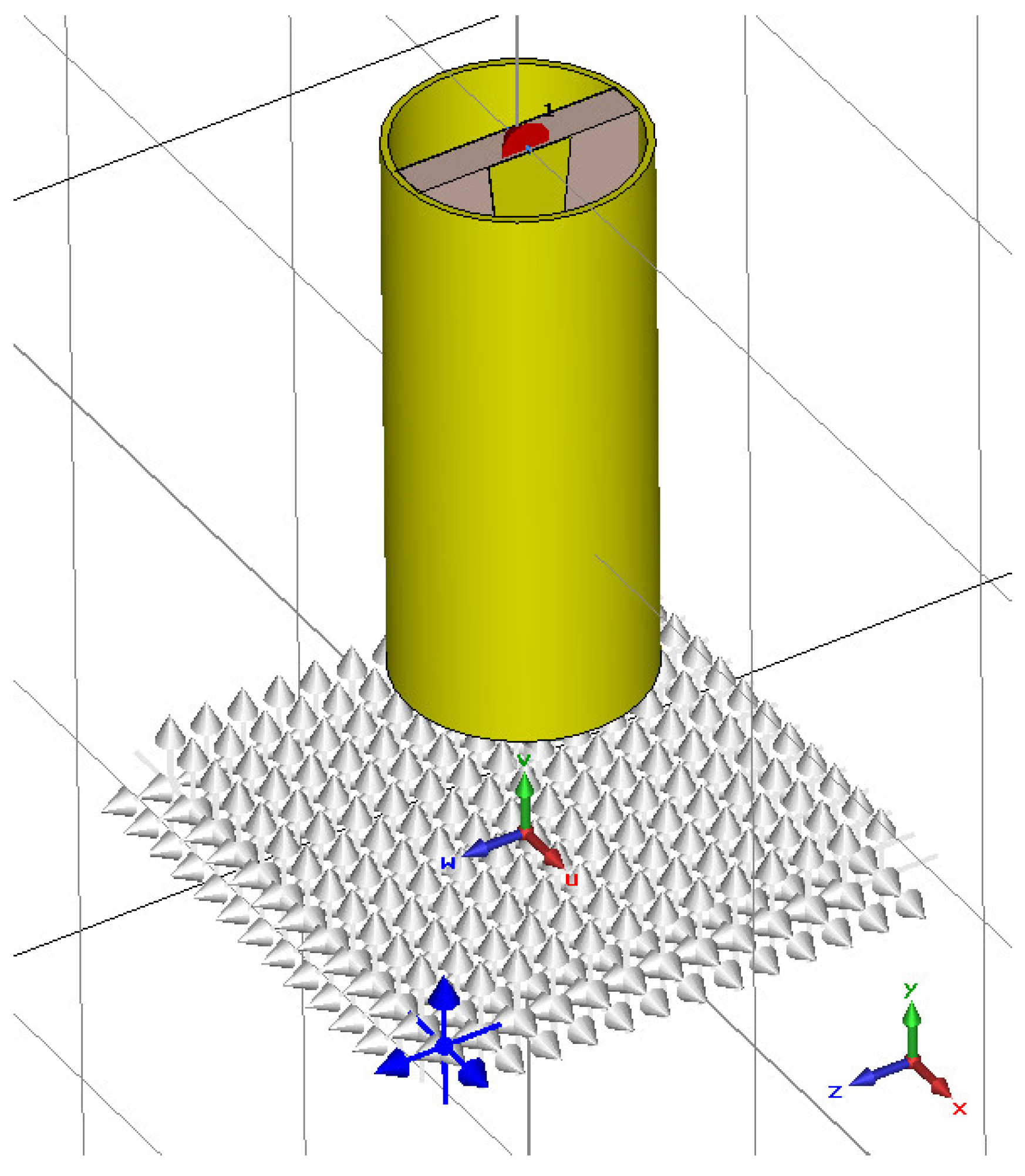
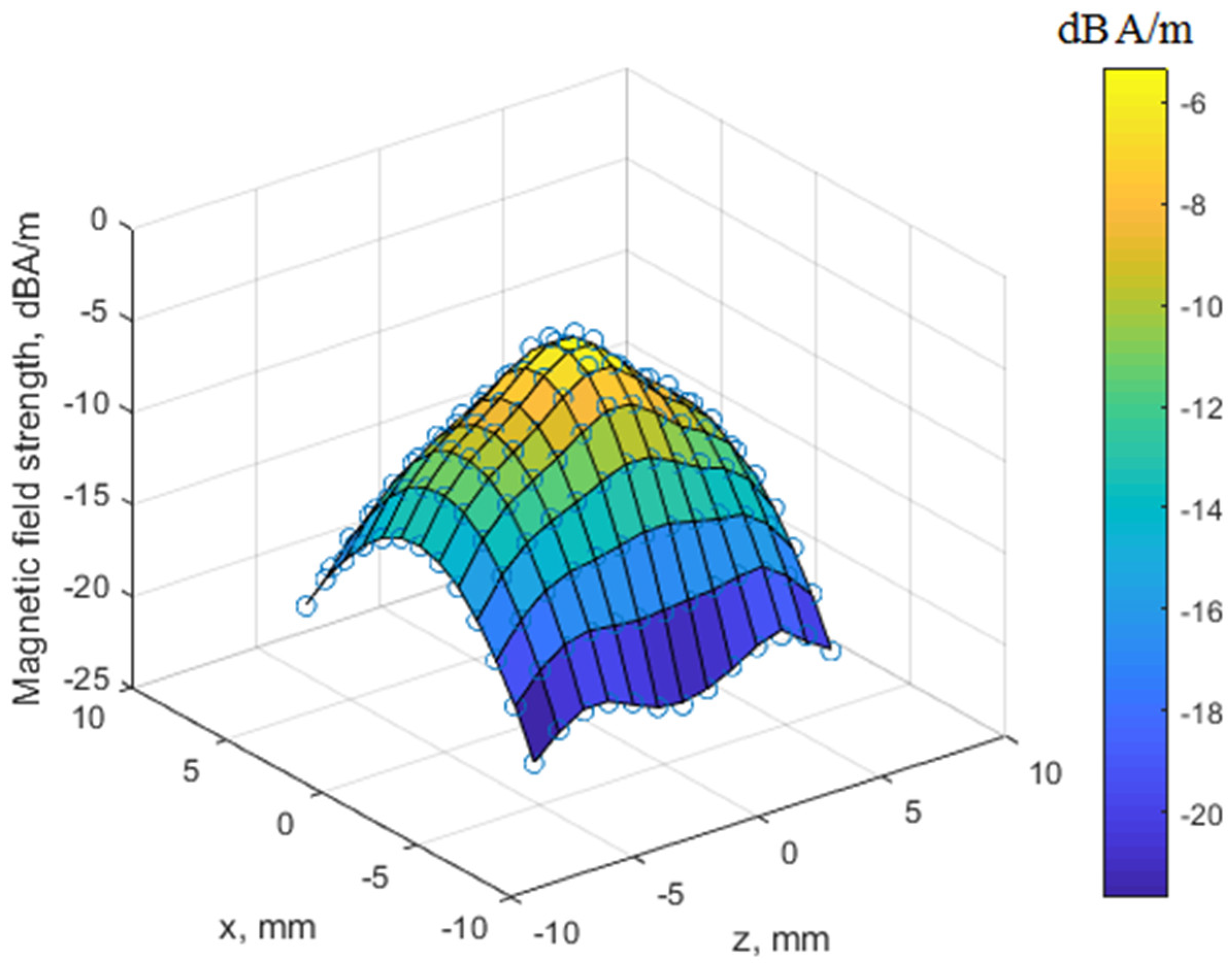
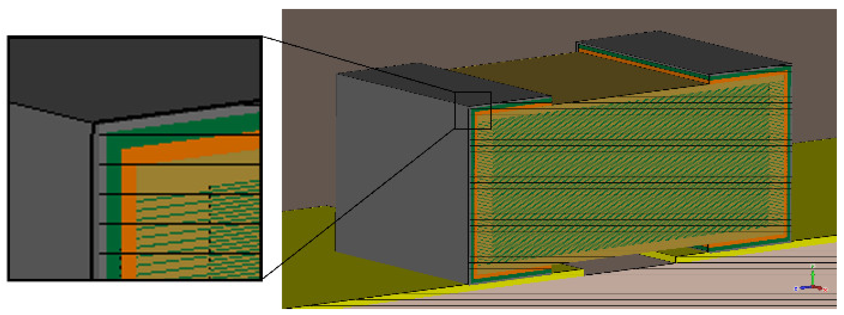
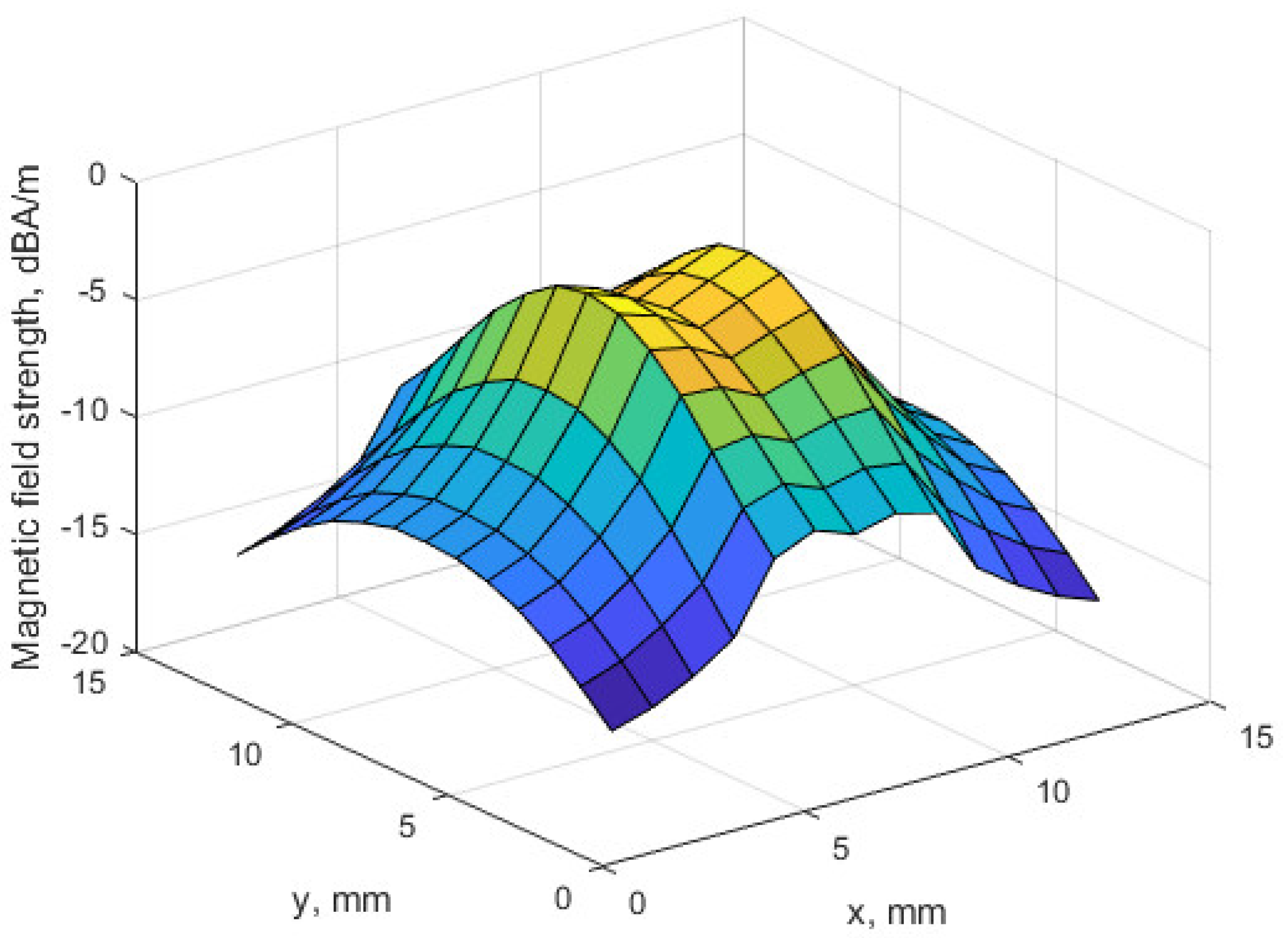
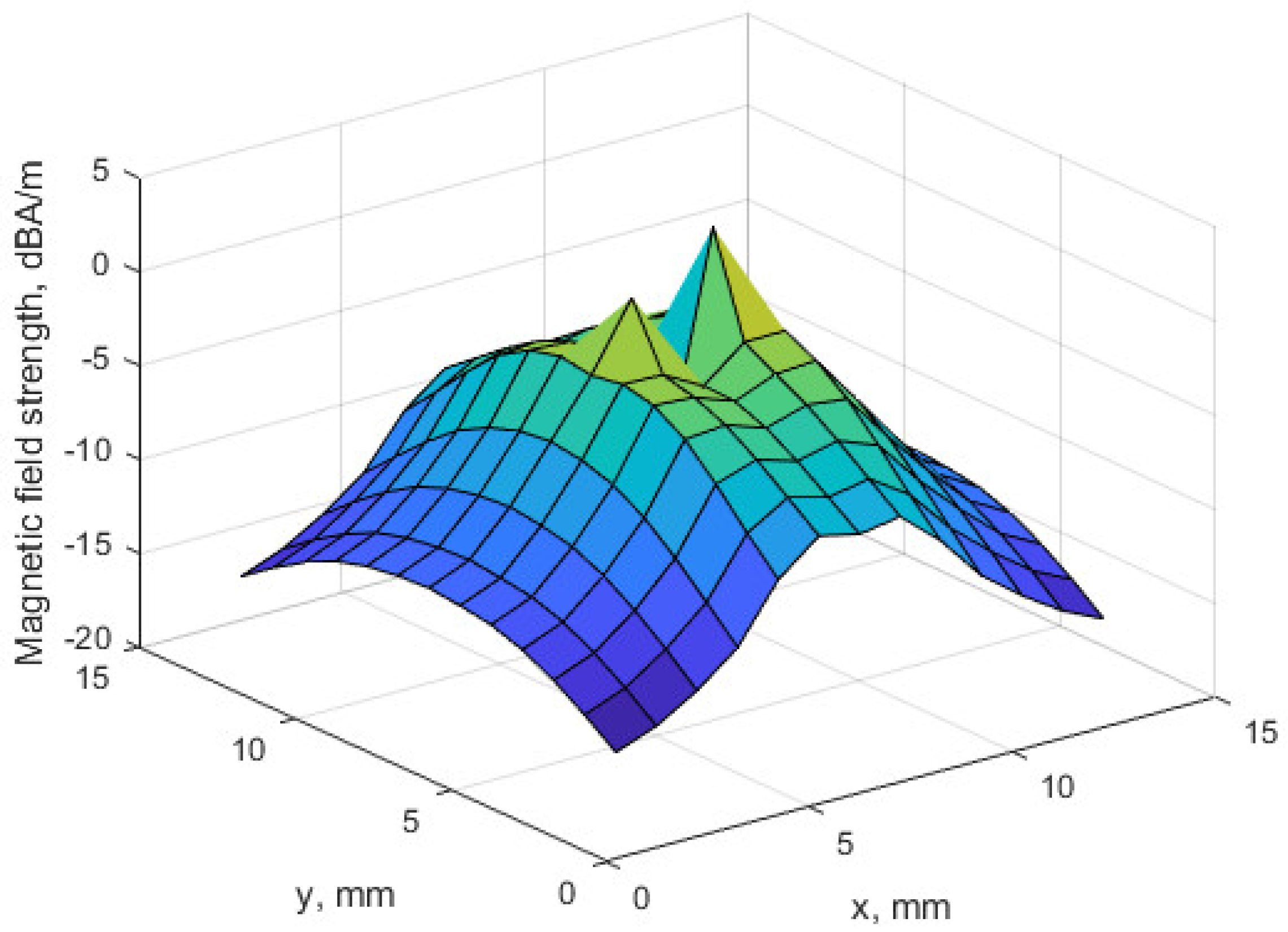
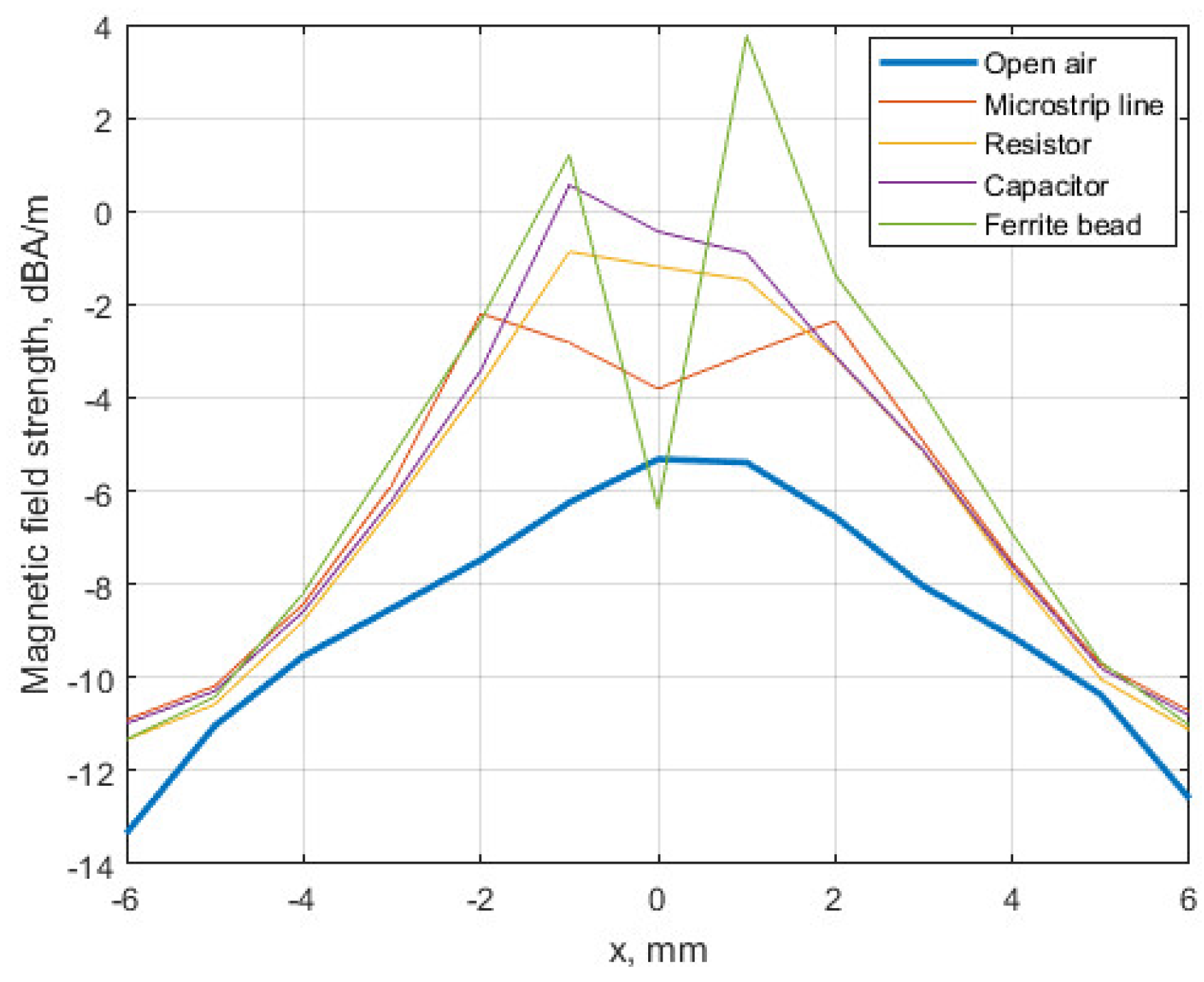
In modern smart and intelligent electronic systems, the electronic devices are exposed to broad spectrum of electromagnetic interferences. In the initial design stages of the electronic devices, the proper solutions for solving the electromagnetic compatibility (EMC) issues are crucial for compliance to the existing standards [
1]. The existing testing methods for the EMC however are not able to spot the susceptible areas of the printed circuit boards (PCBs) and the Pass/Fail report format does not give a detailed insight or the reference for developers of the PCB layout. A variety of the applications and recent research, including the EMC characterization of electrical machines [
2], smart power grid devices [
3], near-field emissions of mobile devices [
4], industrial robotics [
5], automotive equipment [
6], military and avionics [
7] are based on the electromagnetic (EM) field emission mapping method, using the electric or magnetic field (MF) [
8] receiving probes [
4]. The method is able to point the areas with increased EM field emission of the scanned area. However, for more comprehensive characterization of the electronic device solution, the radiated susceptibility mapping has certain advantages, since it is possible to spot the susceptible areas of RF boards where board signal levels are insufficient for effective assessment of the radiated emissions such as RF input stages, shielding, DC power circuitry, ground connections, high speed lines [
9], open loops, or PCB traces [
10], etc. where external disturbances may degrade the performance of a given stage or device in its entirety. The radiated susceptibility mapping resolution improvement and error reducing [
11] are achieved, either by improvement of the probe design [
12], or by post processing the acquired map data [
13]. The electric and magnetic near-field probes for radiated susceptibility mapping exist. However, the magnetic probes are less prone to the proximity of the PCB ground plane and protruding components. The microstrip near-field magnetic probe performance investigated by the authors [
12] yielded to 22–47% improved radiated susceptibility mapping resolution in the 80–3000 MHz range in the proximity of the coplanar waveguide. Due to the PCB landscape and variation of component height, density and magnetic properties, not all areas can be scanned in close proximity, and therefore, the resolution and accuracy of the radiated susceptibility map degrades. The adaptive scenario of the prescanning and successive field susceptibility scanning is beneficial in the suspicious areas of the device under test. The coupling efficiency variations and the probe aperture variations, due to the variable scanning height should be encountered in the pre-scanning stage with the purpose to equalize the injected MF strength at the PCB board level over the frequency range. Based on the previous research and experience gained by authors [
12] in the electromagnetic compatibility field, the adjustable scenario of radiated susceptibility mapping can benefit both from structural improvement of the probe and characterization of its performance under scanning conditions. Hardware adjustments at some degree in the probe RF power stage, such as equalization of the probe frequency response curve or gaining control can be performed, in order to reduce the variation of the coupling coefficient. The probe compensation methods [
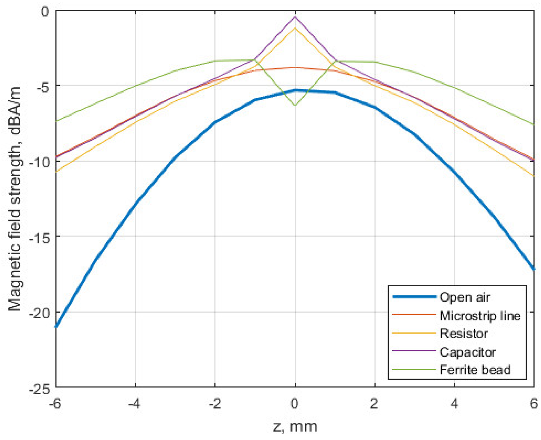
11] or susceptibility map post-processing techniques may be combined for adjustment of the acquired data, and therefore, improve the map resolution. In the radiated susceptibility mapping, it is important to determine the spatial resolution over the frequency range, and to optimize the scanning time and amount of the scanning points. Another important aspect of the radiated susceptibility mapping is to maintain the injected MF strength at the surface of the board within the predetermined levels relevant to the existing standards. Since the PCB components are present in the proximity of the probe, their influence research to the MF strength distribution and to the aperture shape of the improved probe is considered worthwhile by authors. Therefore, the aim of this work is to model the near-field magnetic probe aperture for the improved probe, proposed by authors, and to determine the influence of the PCB structure and component proximity to the performance of the probe in the 80–3000 MHz frequency range. More specifically, the probe aperture map, its distortions and spatial resolution will be assessed by means of simulation, and the susceptibility pre-mapping measurement results will be presented in this work. The recommendations for the near-field probe MF map distortion assessment will be given. The paper is organized as follows. In the Chapter 3, the model of the near-field magnetic probe and the simulated near-field MF strength in open-air conditions of the probe are presented. The reference MF aperture map is defined and the detailed models of the passive components are given. Chapter 4 is dedicated to the simulation of the MF map distortions due to the presence of the passive components in the proximity of the improved probe. The experimental application of the probe is demonstrated in in the Chapter 5. Pre-scanning and detailed scanning results of the radiated susceptibility map are presented, followed by discussion and conclusions. The list of abbreviations provided in
Appendix A,
Table A1.

 ,
, 
