Review

Ensuring the Reliability and EMC by Modal Reservation: A Brief History and Recent Advances

by
Adnan Alhaj Hasan
and
Talgat Rashitovich Gazizov
*
Scientific Research Laboratory of Basic Research on Electromagnetic Compatibility, Tomsk State University of Control Systems and Radioelectronics, 634050 Tomsk, Russia
*
Author to whom correspondence should be addressed.
Symmetry 2022, 14(11), 2466; https://doi.org/10.3390/sym14112466
Submission received: 10 October 2022 / Revised: 12 November 2022 / Accepted: 16 November 2022 / Published: 21 November 2022
(This article belongs to the Section Physics)

Abstract

:
With the growth of the radioelectronic complexity and the demand for cutting edge devices, the need to protect them and increase their reliability is also rising. There are many methods to provide this. Modal reservation is one of the most effective, reliable, and least complicated methods used nowadays. Using this method in tracing and mounting of printed circuit boards can guarantee both electromagnetic compatibility (by using modal filtering) and reliability (by using the cold redundancy) of the final electronic device. Modal reservation was proposed in 2015, and since then, massive research has been conducted on its investigations and development including 18 patents for inventions. Most of these studies have been devoted to modal reservation in terms of conducted emissions. However, up to now, a general and comprehensive review of modal reservation and investigations of its application with respect to radiated emissions has not been performed. Therefore, this paper aimed at presenting such a review on the history and recent research on modal reservation, concentrating on the studies related to radiated emissions. In addition, this paper analyzes current studies on the efficiency of using modal reservation under climatic impact.

1. Introduction

A highly reliable system requires that engineers should increase component reliability (for example, changing the component material) or apply redundancy methods using the existing resources without violating the system’s cost, weight, and volume constraints [1,2]. The second choice is preferable because of its simplicity [3] and its first implementation is referred in the literature to the work conducted in 1956 [4]. Redundancy (later in this work, it will be referred to as reservation) is likely to be applied in critical systems where uninterrupted operation is required, and the maintenance is difficult and expensive, for example in the case of onboard radioelectronic systems. In this case, the mission time of communication satellites may last for more than 10 years [5]. Systems or subsystems may be reserved in active or inactive mode with lower failure rates, since the reserved components will be in standby mode until failure [6]. In addition, those reservation types can be combined and divided into sub-types: parallel and k-out-of-n active reservation types, and the cold, hot, and warm standby reservation types [7,8]. Reservation can be employed not only to improve a system’s reliability, but also its efficiency [9]. Moreover, reservation is considered to be a quick solution to achieve any desirable level of reliability in the early design stage [10]. Since reservation can be performed in different forms, the optimized design of the system can be obtained by reaching the balance between the system’s cost and reliability. Several works have been devoted to developing mathematical models to determine system reliability [11,12,13], even in real-time applications [14]. Reservation in all its types has been used in different fields. It has been employed in information protection [15], memristive devices [16], and in neural networks [17]. It has even been employed in nanotechnology which has a high defect rate [18,19]. Moreover, this technique is also popular in space [20,21] and aviation [22] applications, and in modern systems related to unmanned aerial vehicles, for example to protect their datalink [23]. Reservation is also used in communication applications [24]. The printed circuit board (PCB) failures can lead to critical problems and have various causes such as aging, heating, and insulting [25]. To manage these failures, reservation should be commonly used in PCB design. Several works have described the use of this technique for this purpose [26,27]. However, reservation is not always useful, for example, if the system is not designed to deal with artificial or natural electromagnetic interference (EMI), that can be caused by reservation itself [28]. Thus, ensuring electromagnetic compatibility (EMC) in PCB design, even when the design includes reservation, is unavoidable when dealing with electromagnetic disturbances [29,30]. Some researchers have tried to increase the reliability of PCBs with reservation taking EMI into account [31], but there was no comprehensive way to do this [32,33]. In general, one can say that all traditional ways to deal with EMI consequences are not highly effective especially against ultrashort pulses (USP) [34].
Modal reservation (MR), considered in this work, is a method that can both improve the reliability of radioelectronic devices using cold standby reservation and ensures their EMC by using the so-called technique of modal filtering [35]. Modal filtering is used to protect radioelectronic devices from USPs; it is also used as a method to detect and diagnose contactless electrical connections in hidden walls [36]. MR can also be used in different applications. However, the most important application of this method is in critical and onboard radioelectronic devices. For example, MR is used to increase noise immunity of digital signal processing units [37] and power systems [38] of spacecraft autonomous navigation systems. This method has several types: based on the multiplicity of redundancy (single, dual, triple, … n-tuple) [39], based on the structure symmetry (symmetrical and asymmetrical) [40], and based on the target item (PCB trace or components, cable, dielectric) [41]. Most of these types have been extensively investigated in terms of conducted emissions. To fully explain the mechanism of this method and interpret its consequences, it is also necessary to study its characteristics in terms of radiated emissions (RE). This has been reflected in only a few works [42,43,44,45], where such investigations were performed using only the analysis of simulation results and without taking into account climate impacts.
The aims of this paper are to review the history of MR by providing a comparative evaluation of the manufacturability, applicability, and effectiveness of the use of MR-based structures, to review recent research related to estimating RE from PCBs with single MR, and to analyze and demonstrate the latest studies on this issue taking into account climate impacts.
This paper is organized as follows: Section 2 provides information about the history of MR and the basic research that has been conducted, including all the obtained patents for inventions. Section 3 is devoted to reviewing recent research results related to the investigation of RE from MR-based structures. Section 4 presents, compares, and analyzes the results of current research related to the estimation of RE from MR-based structures under climate impacts which have not yet been published. Section 5 summarizes all the advantages of MR and concludes the main outcomes of the paper.

2. The History of MR

In general, MR consists of PCB tracing where the reserved and reserving PCB conductors are traced in such a way that strong electromagnetic coupling is achieved between them in an inhomogeneous dielectric medium. This allows using the advantages of modal filtering and exploiting modal distortions to suppress conducted USPs. These pulses have a strong penetrative capacity due to their short duration, high power, and wide spectrum. Modal decomposition is achieved if the USP duration is less than the absolute value of the difference in even and odd mode delays in the structure with coupled conductors. In this case, USPs are decomposed into pulses with smaller amplitudes. Therefore, the main PCB is protected and its electromagnetic compatibility is guaranteed. Moreover, if the reserved PCB experienced any sudden failure, the reserving one will immediately initiate operation without affecting the functionality of the device. In this manner, the reliability of the device will also be increased, which can be determined by the redundancy multiplicity and the failure probability of each reserved PCB. Table 1 shows a general comparison of MR with other EMI protection methods. As can be seen, MR outperforms possessing a number of advantages. The only disadvantage is the difficulty of MR implementation. However, it is hard to evaluate the complexity of MR industrial implementation because it is still under scientific research.
The idea of MR was first formulated in 2015, and the first works on MR were published in 2016. In what follows is a retrospective review of all the MR methods. All the obtained patents on MR are presented in Table 2, and later in the text are referred to by their sequence number (No.) in the table. The first patent for a method of tracing printed circuit conductors with reservation was obtained in 2016 (No. 1 in Table 2). This method, which is the simplest one (Figure 1), was able to reduce the USP amplitude by two times. In the same year, another method to trace the PCB was presented (No. 2). The reduction of the USP amplitude in this method is also by two times, but it differs from the previous one by the fact that the gap between the reserved and the reserving conductors is filled with a dielectric material with a relative dielectric permittivity (εr) greater than the one used in the PCB substrate material (Figure 2). Since the value of εr can affect the difference in the per-unit-length delay of the odd and even modes, increasing εr can be used to raise this difference, thus improving the efficiency of modal filtering. In the method proposed in (No. 3), the reserved and reserving conductors are placed under each other in a symmetrical way relative to the substrate, and the remaining reference conductors are electrically connected to each other (Figure 3). The USP amplitude reduction is also reduced by two times. The same can be achieved by using the method proposed in (No. 4), but the later can also guarantee a PCB mass reduction by removing one reference conductor. However, this configuration does not increase USP suppression (Figure 4).
In (No. 5), another method was proposed, and it differs from the one in (No. 1). More specifically, each of the two conductors in its structure forms a turn of a meander line, and together they form a segment of the four-wire transmission line (Figure 5). By using this method, the USP amplitude can be reduced by four times. In this method, the like-named conductors of the reserved and reserving circuit traces form a coupled transmission line with different values of per-unit-length delays. Each conductor pair is connected to each other at one end in one of three ways, which can be seen in Figure 5: on one layer (conductors 1–2 and 1*–2*), on different layers (conductors 1–1* and 2–2*), or diagonally (conductors 1–2* and 2–1*). In addition, and based on using different dielectric materials, another two MR methods were proposed in (No. 6 and No. 7). The first one was an improvement of (No. 1, No. 2 and No. 3) and consisted of increasing the reliability by raising reservation multiplicity and interference immunity by increasing the duration of the USP which is decomposed completely (Figure 6; any conductor in figure can be an active one). The second one guaranteed the same but with the possibility of two-layered PCB routing: the outside and inside signal layers (Figure 7).
Another method similar to those in (No. 1 and No. 5) has been proposed recently (No. 8). In this method, the reserved and reserving PCB conductors are traced in pairs, parallel to each other on each of the two main layers with a minimum acceptable gap between them. The reference and power conductors are made in the form of separate layers between the main layers. Here, not only are the signal conductors of the PCBs reserved, but also the power conductors; all of them form coupled lines in the gaps formed in the reference (Figure 8). This method can reduce the susceptibility of the reserved power conductors to external conductive emissions and reduce the level of conductive emissions from them.
The method in (No. 9) was based on the mutual arrangement, layout, and tracing of the reserved and reserving PCBs. It differs in that the reference conductor is made in the form of separate layers on the reserved and reserving PCBs, which are bonded together by a dielectric layer with εr greater than that of the dielectric substrates of the reserved and reserving PCBs (Figure 9). Both boards are located in parallel and under each other, and the PCB electronic components are placed on opposite sides of the bonded boards. The USP amplitude reduction is 2.5 times. The disadvantage of this method is a difference in traceability of the reserved and reserving boards caused by asymmetric position of radioelectronic component pins relative to the dielectric layer. This layer bonds the reserved and reserving boards so that like-named component pins are not under each other. Because of this, the length of the segments of coupled lines formed by the same-type traces of the reserved and reserving circuits are reduced. This in turn reduces the useful mutual influences due to the electromagnetic coupling between the reserved and reserving like-named traces of the reserved and reserving boards. In (No. 10) the proposed method differs from the previous one in (No. 9) in that the molding of the reserved component pins is performed in one direction relative to the component body plane, and the reserving components—in the opposite direction (Figure 10). The reserved and reserving electronic components are placed under each other, which results in a reduction in the susceptibility of the reserved board to internal and external conducted emissions (on the board and from it) (Figure 11). Additionally, in (No. 11) another method was proposed. The uniqueness of this method is in the fact that the reserved and reserving components are placed not on the outer, but on the inner sides of the reserved and reserving PCBs in the layer of bonding dielectric (Figure 12). The USP amplitude reduction using this method achieves 2.25 times. The method proposed in (No. 12), is a method of reservation of flat cables. It differs in that the conductors of the reserved cable are placed at one level, and those of the reserving cable—at another. At the same time, the like-named conductors are placed under each other in the dielectric layer (Figure 13).
In (No. 13), the method of triple MR of circuits was proposed for the first time. It is similar to the PCB arrangement method in (No. 9) but differs in that two additional reserving circuits are introduced. In this way the corresponding parts of the reserved and reserving circuits are laid out in parallel to each other in a dielectric bonding layer, so that the reserved and one reserving circuit are on the reserved board and the other two are on the reserving board (Figure 14). The USP amplitude can be reduced by 4 times using this method. In (No. 14), another method of circuit triple reservation was proposed. It is similar to the method in (No. 3) but differs in that each signal conductor is divided by a gap into two identical conductors (Figure 15). Comparative studies on using these methods have been performed. For example, in [46] the authors proved that using the MR method from (No. 3), an attenuation coefficient of the interference signal up to 12 dB can be achieved, and they compared the results obtained using this method with those obtained using the methods from (No. 1 and No. 9). By implementing MR on the digital signal processing unit of a spacecraft autonomous navigation system, they estimated the improvement of its noise immunity.
In contrast to (No. 13 and No. 11), in (No. 15) another MR method was proposed to provide mutual arrangement, layout, and tracing of the reserved and reserving boards with a reference made as two separately printed conductors in the dielectric layer which glues the boards together (Figure 16). This simplifies the PCB manufacturing and mounting of its components and reduces the susceptibility of the reserved circuit to externally conducted emissions. In addition, in (No. 16) another mutual arrangement MR method was proposed. It differs from (No. 9) in that it proposes additional signal layers such that the reserved and reserving conductors of the same circuits are traced on the outer and inner signal layers of the PCB connected by vias (Figure 17). However, here, the reference is made as separate layers where each of the reserved and reserving PCBs are made from two dielectric layers.
As one of the main essences of MR is reliability, it was also necessary to study the efficiency of MR after failure. Therefore, in [47] the immunity to USP excitation for PCBs with single and triple MR was studied after short and open circuit failures. The analysis showed that, with single MR, the attenuation after failure decreased by 1.7 times. When using triple MR and after failure, it was found that it is preferable to switch to a circuit whose electromagnetic coupling with the reserved circuit is less. This is explained by the fact that deviation of the decomposed pulse amplitudes in the case of failure at the end of one of the reserving conductors from the amplitudes before failure is minimum. These and other results were discussed and confirmed for a single MR in [48], not only in the time domain, but also in the frequency domain of up to 2 GHz in [49], and also up to 18 GHz using quasistatic and electrodynamic analyses to verify the results obtained experimentally in [50]. The switching order after failures for double MR was discussed in [51]. The case of switching after failure was also studied in detail for triple MR in the time and frequency domains [52]. Based on these studies two patents were obtained on methods of after failure switching for double MR (No. 17) (Figure 18) and triple MR (No. 18) (Figure 19). Moreover, the investigation showed that the failure probability of the reserving trace when using MR is lower than that of the reserved one. This was proved in [53] for single MR and in [54] for triple MR, using the five N-norms [55] which are used to estimate the threat of USPs on radioelectronic devices.

3. Recent Research on RE from PCBs with MR

The following is a review of the recent studies and their results related to the investigation of REs from structures with MR. This review was carried out to estimate and evaluate the efficiency of MR in terms of RE. All the results have been presented at different conferences and will soon be published. In addition, they form a necessary base to investigate the effect of climate conditions on REs from PCBs. As mentioned above, the RE from PCBs with MR has not been studied in detail except for a few works. Recently in [42], the authors proposed an algorithm based on the combined use of quasi-static (to calculate the current along the conductors) and electrodynamic (to calculate the field components) approaches to obtain the far field electric intensity from a test structure with MR. This algorithm provided sufficiently accurate results with less computational costs compared to the separate use of each approach. The current distribution and the radiation pattern obtained using the electrodynamic approach [56] and those obtained using the proposed algorithm were compared and showed good consistency. The algorithm was also tested on wires with dielectric insulation [43]. The study demonstrated that increasing the dielectric permittivity, the wave impedance of a single wire decreased, and the current amplitudes increased compared to their values from a wire without insulation. An asymmetrical radiation pattern and a change in the main maximum direction were also revealed and explained by the current amplitude growth in the first segment of the wire and the current phase shift along the wire. The same observations were noticed in the case of coupled wires, but increasing the insulation dielectric permittivity, the asymmetry of the radiation pattern decreased.
The first analysis of the MR implementation effect on PCB RE was presented in [45] using the above proposed algorithm and comparing the results [44] obtained using the finite difference time domain method in another software. These preliminary simulation-based studies on a test structure proved that the use of a single MR reduced the RE by up to 10 GHz because of the electromagnetic coupling between the reserved and reserving conductors in an inhomogeneous dielectric medium. This is explained by the appearance of even and odd mode currents in opposite phases, which decreased the currents in the conductors and electric field strength from the contribution of these currents in the far field at certain frequencies. Thus, at these frequencies, a decrease in RE, as well as a decrease in susceptibility to radiated electromagnetic fields, can be expected. On the other hand, there are frequencies or directions where the opposite is noted, which might be associated with resonance shifts and field redistribution.
To prove the above conclusions, an experimental study in the far or near field is required. However, these types of experiments are expensive, not informative (for example, in the far zone for such structures), and not feasible for academic purposes. Therefore, we recently started our preliminary studies using another approach to estimate the RE from PCBs with MR. Since there are various types of MR tracing and layouts, we started with the simplest MR type from (No. 1). To imitate the layout of a PCB without MR, we used the structure of a single microstrip line, and to imitate the layout of a PCB with MR, the structure of coupled microstrip lines was used. Figure 20 shows the cross-sectional parameters of the structures under study. The notation (l) refers to the length of each conductor, (w) to the width, (t) to the thickness of each conductor, and (s) refers to the distance between the conductors. The substrate thickness is referred to as (h). The material used was foiled heat-resistant fiberglass [57] known in Russia as (STF), with a relative dielectric permittivity (εr) of 4.7–5.5 and dielectric loss tangent (tgδ) of 0.017–0.035 at the frequency of 1 MHz. The notation (d) refers to the distance from the edge of the dielectric to the active conductor. The equivalent schematic diagrams of these PCBs are presented in Figure 21 and their manufactured prototypes in Figure 22. The PCBs had dimensions of 98 × 98 mm. The distance of the margins from the tap to the subminiature version A of connectors (SMA) was 10 mm at each side.
Firstly, we modeled these structures in the TALGAT software [58] and obtained the frequency dependences of their S-parameters [59]. The simulation was carried out at different values of εr, without taking the losses in conductors and dielectric into account. We measured the frequency dependences of the S-parameters using the vector circuit analyzer R&S ZVA 40 (two ports) which was connected to the PCB SMA connectors via the R&S ZVZ195 and Semflex 60637 measuring cables passing in the climate heat–cold chamber SPEC SU-262 to fix the temperature at 23 °C (Figure 23). Then, we compared the calculated and measured results. They showed good agreement, with an average difference between them being up to 5 dB. We found that the transmission ratio for the PCB with MR was lower than without it because of the modal decomposition effect. However, this reduction will not affect the useful signal as the values of the transmission ratio remained higher than −3 dB (for the pass band) except for some frequencies of the frequency range under study, due to the frequency shift. After this, we decided that it was also necessary to have information about the MR effect in the case after short (SC) and open (OC) circuit failures. Therefore, we considered two other structures with the same parameters as in Figure 20. Their equivalent schematic diagrams and manufactured prototypes are presented in Figure 24 and Figure 25, respectively. In the same manner, the frequency dependences of the S-parameters for all the boards measured and calculated at different εr and tgδ values were obtained and compared and demonstrated consistency [60]. We estimated the changes in |S21| and |S11| after SC and OC failures compared to those obtained for the PCB with MR (0.09, 3.9 dB and 0.16, 5.31 dB) and without it (0.35, 5 dB and 0.53, 2.86 dB).
After this, the RE levels from PCBs with MR were estimated before and after experimental failure. To do this, we used classical [61] and miniature [62] TEM-cells (Figure 26). Such TEM-cells are based on the coaxial transmission line of a rectangular cross-section and are widely used for testing interfering emissions and immunity of integrated circuits. When a generator supplies a signal with pre-defined characteristics to the input of the tested device placed in the regular part of the cell, a transverse electromagnetic wave propagates in the inner space of the cell forming a homogeneous electromagnetic field. Then, the signal can be absorbed by a matched load located on the opposite side of the cell next to the microwave connectors. The first resonance frequency of the TEM-cell is determined by its geometric parameters, which in turn determines the upper boundary of the operating TEM-cell frequency range.
Using both TEM-cells, the classical (up to 2 GHz) [63], and the miniature (up to 5 GHz) [64], the frequency dependences of the voltage amplitude levels at the central conductor (CC) for all boards were obtained at room temperature using the VNA R&S ZVA 40 (four ports), Cascade microtech measurement cables (124-084-B), and RF Cable Assemblies 40 GHz 25”Lng VNA Conn Ends 2.92 mm (FD0BS0HR025.0) (Figure 27). The measured results obtained after failures were compared to those obtained before them. The comparison results demonstrated that the voltage amplitudes at the TEM-cell CC input and output for the PCB with MR were lower than for the PCB without MR by about 10–20%, except at some frequencies of the studied domain, because of the frequency shift. This means that the level of RE from the devices was also lower because it is proportional to the voltage amplitudes, which gives the PCB with MR an advantage over the PCB without MR since it can lessen RE, especially at high frequencies. After failure, it was found that, at low frequencies, failures had almost no effect on the level of RE. However, at high frequencies, after OC, it became even higher for the PCB without MR, and after SC failure, it was lower, even before failure.
Next, we obtained the frequency dependences of the S-parameters for all PCBs at different temperatures in the climate chamber [65,66,67]. Estimating these characteristics can provide a prediction about the operability of these structures under any climate conditions. We found that, in general, the S-parameters of the prototypes decreased with increasing temperature and increased with decreasing temperature, compared to the results obtained at room temperature over the entire frequency range except for the resonance frequencies. We observed that at low temperatures, there was a noticeable shift in the resonances towards higher frequencies with a decrease in the |S21| values and an increase in the |S11| values. At high temperatures, the shift in resonances was observed towards the low frequencies with a decrease in the |S21| values and increase in the |S11| values. This is explained by the change in characteristics of the transmission line with changing temperatures, because of the change in the dielectric permittivity and the geometric parameters of the transmission line. In general, the transmission coefficients for the PCBs with MR before and after failure were smaller than those for the PCBs without MR. After failure they were less than before failure, in almost all of the investigated frequency range. The reflection coefficients after the SC failure were, in general, lower than before failure and without MR, and after OC failure, they were higher than before failure and for PCBs without MR. Moreover, the effect of MR remained after failure without affecting the useful signal except at high temperatures where the operating frequency range of the useful signal decreased considerably. Furthermore, there was a shift in resonances by up to 0.4 GHz towards the low frequencies after SC and towards higher frequencies after OC failure. This happens because of the reflection at the line ends, which increases the difference between them near the resonance frequencies. Table 3 summarizes all the previous research.

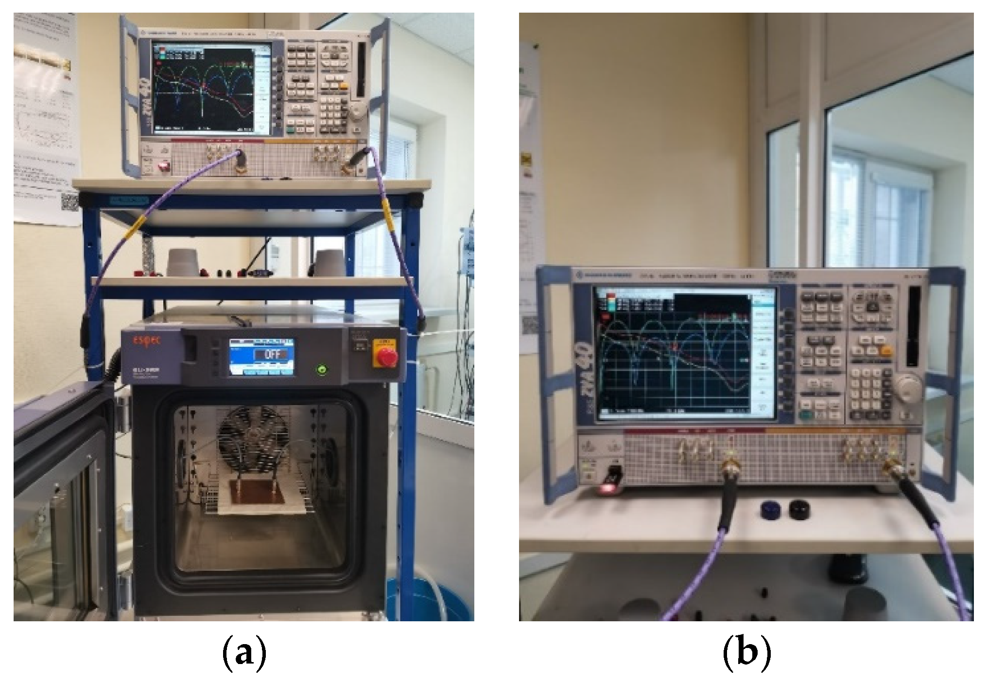
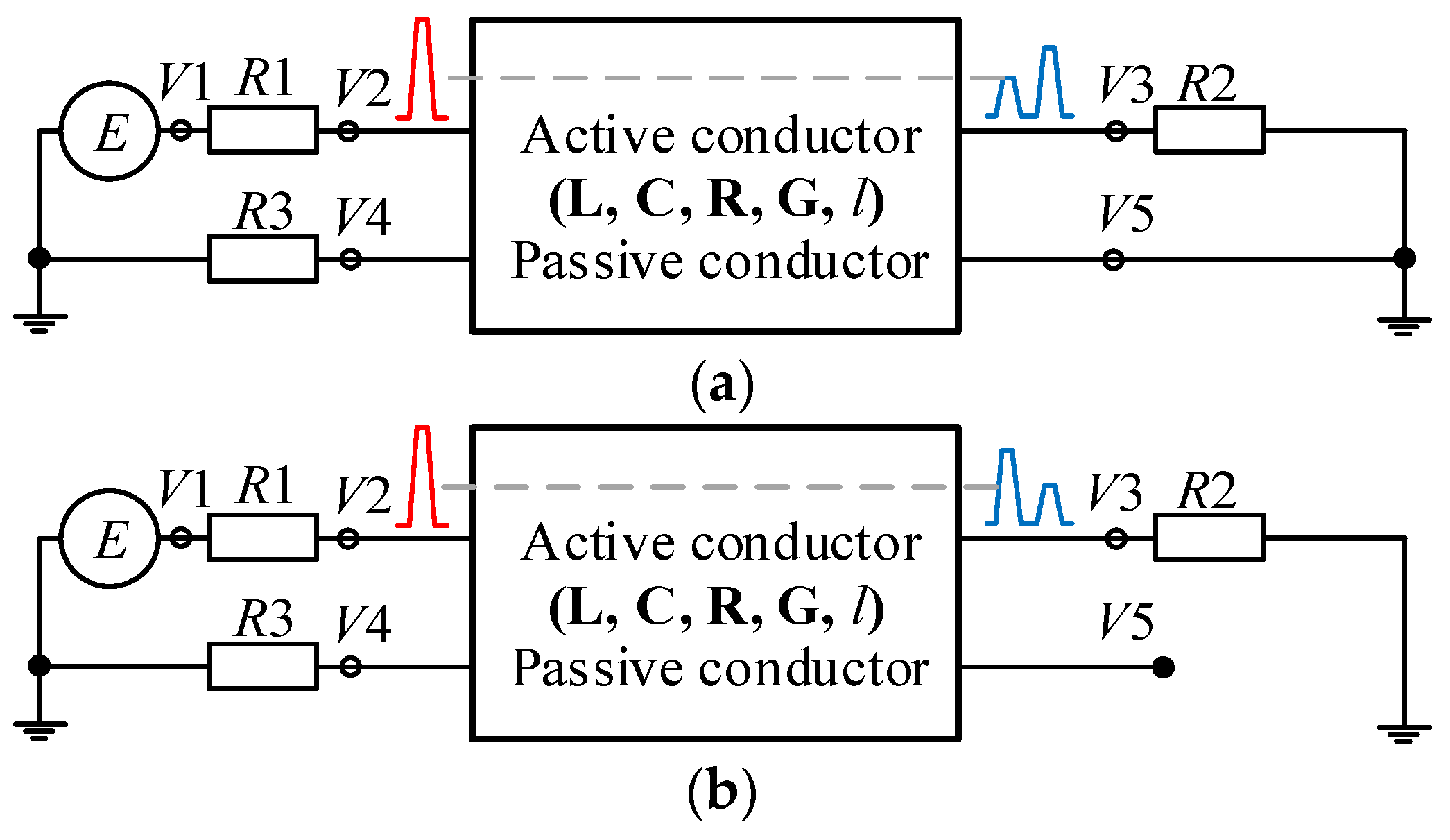
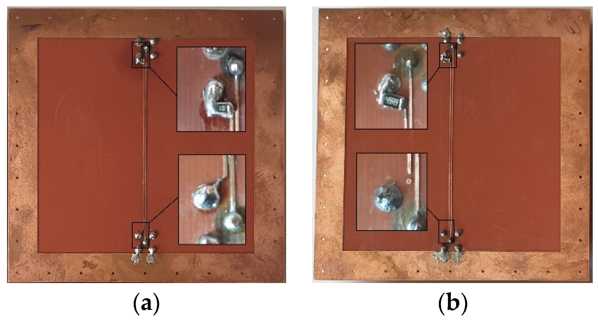
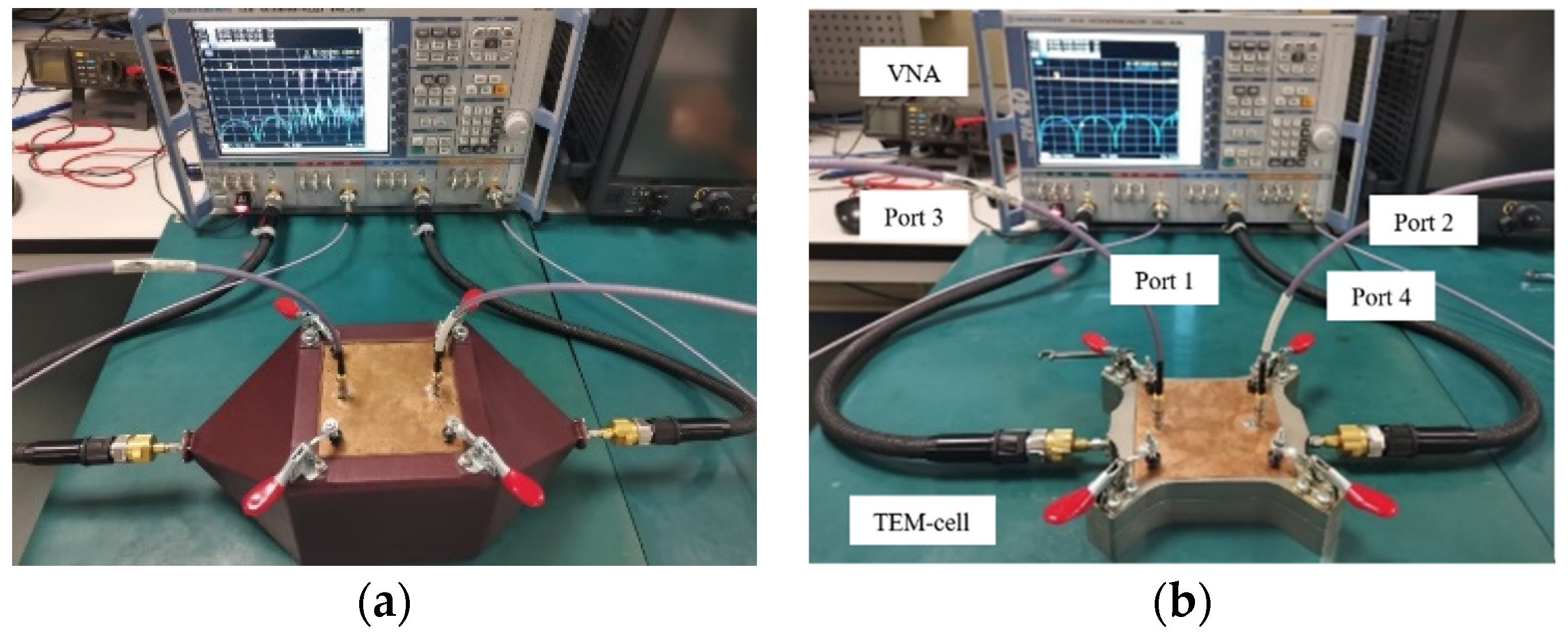
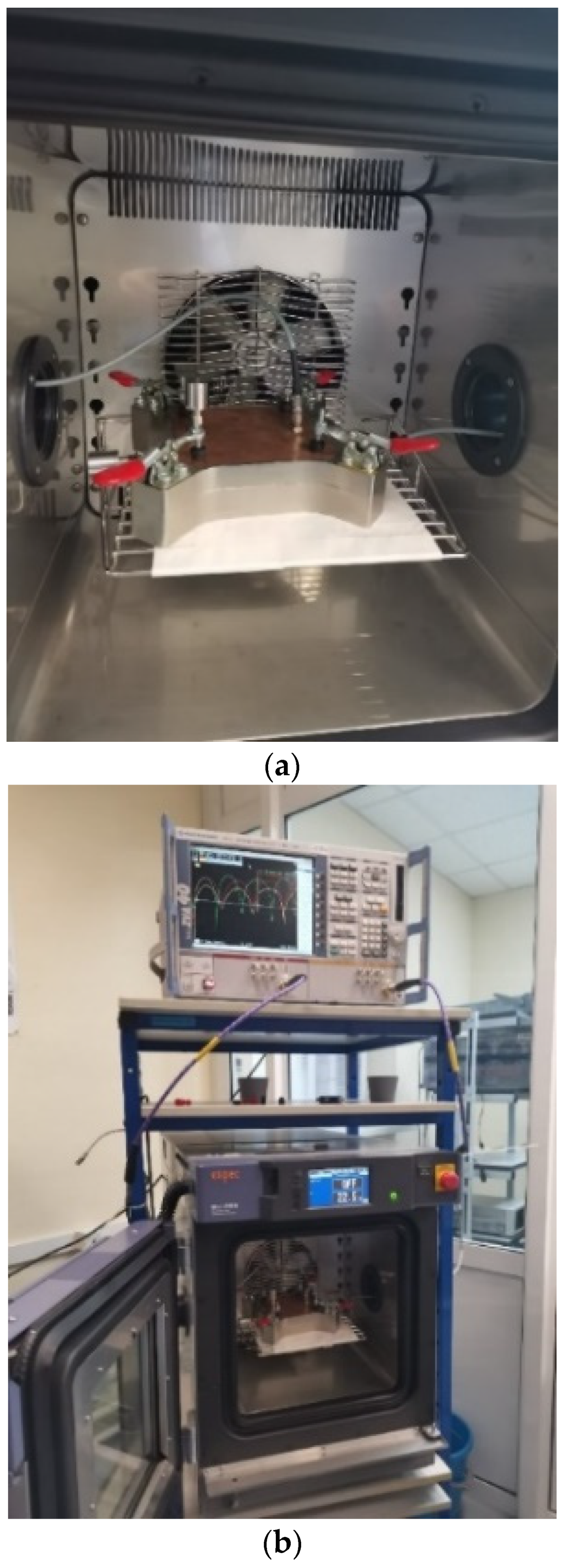
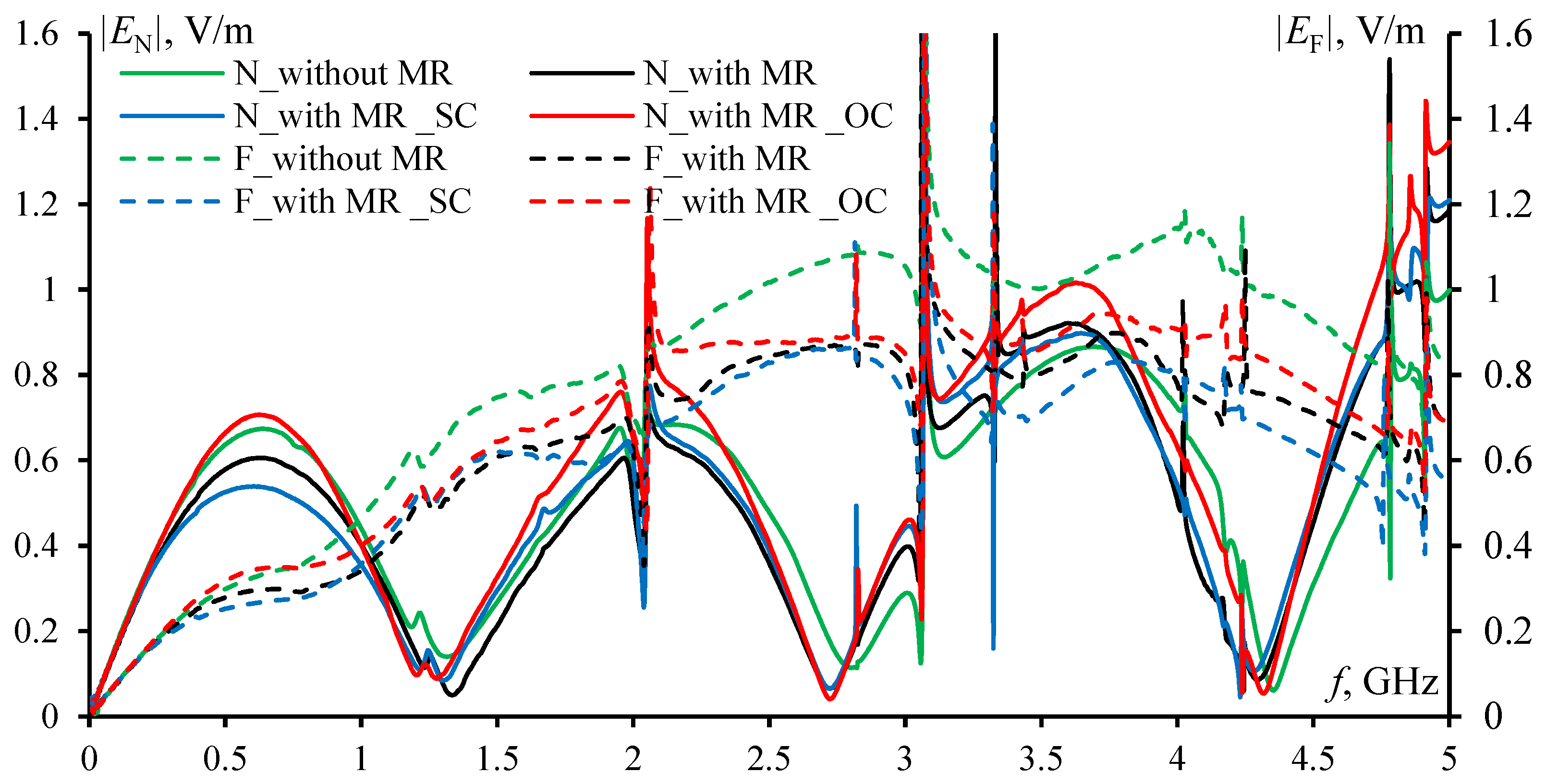
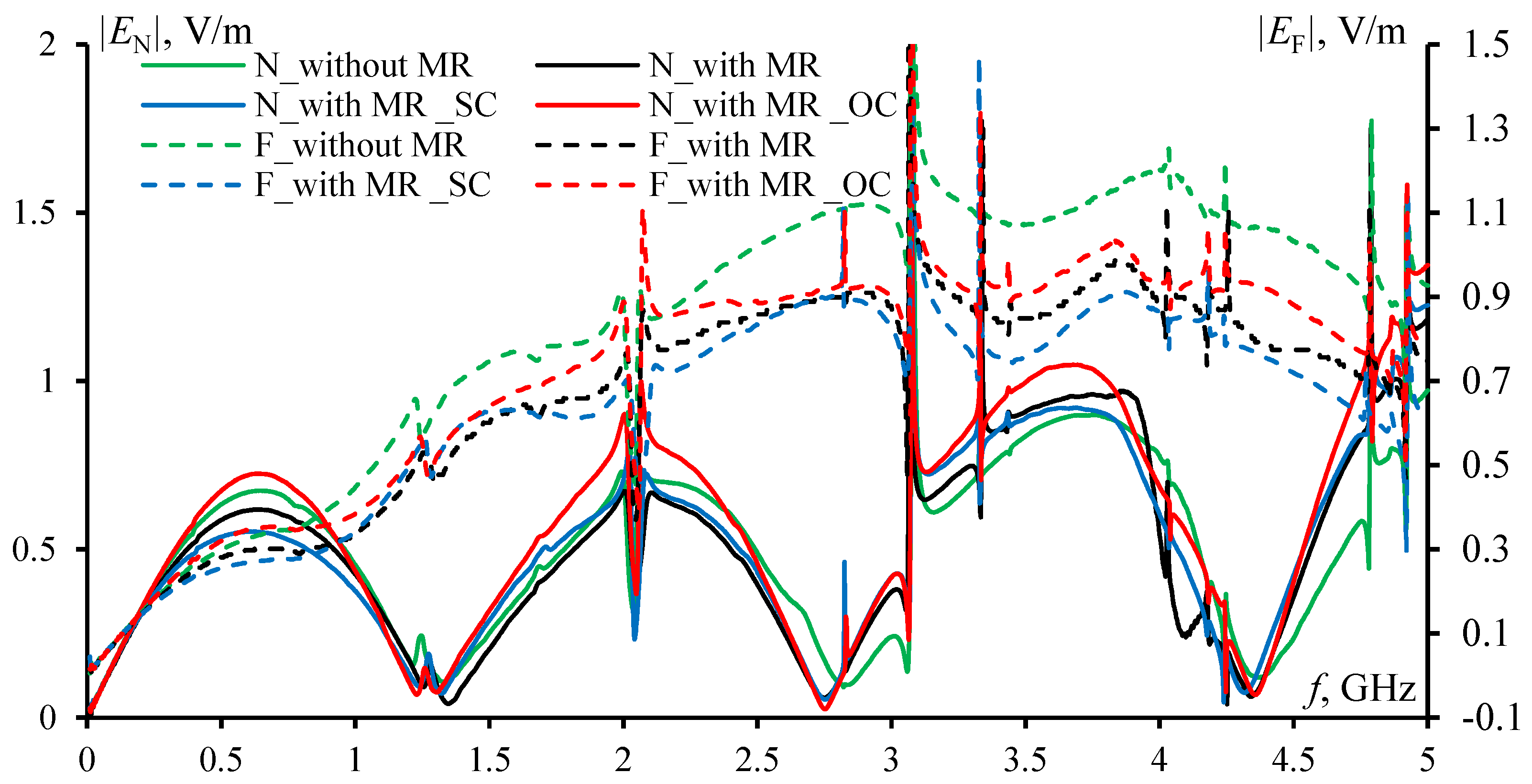
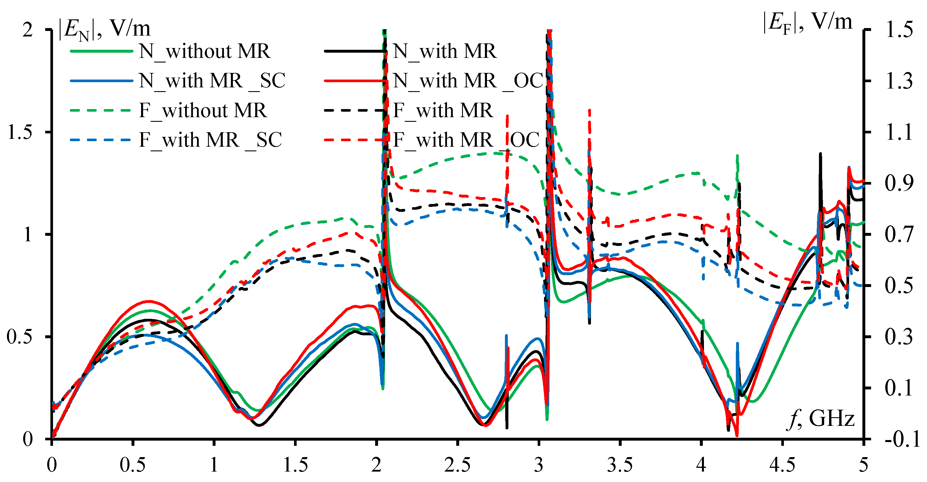
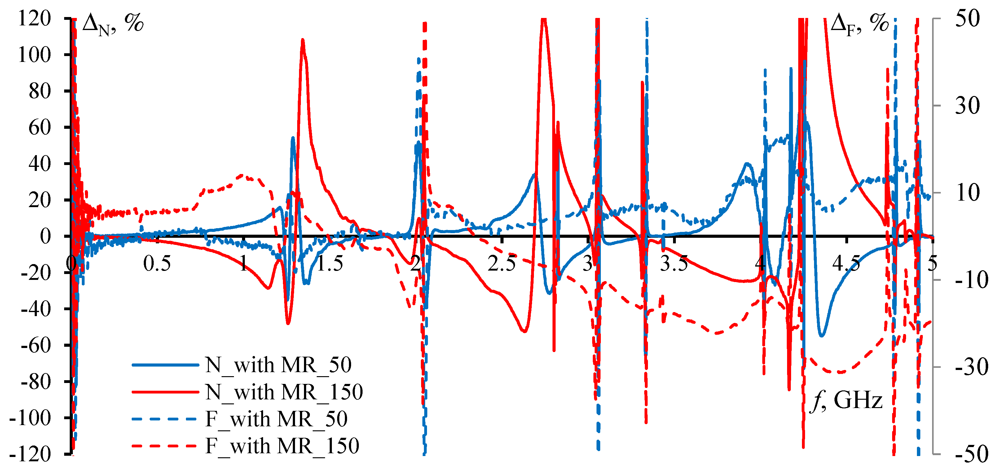
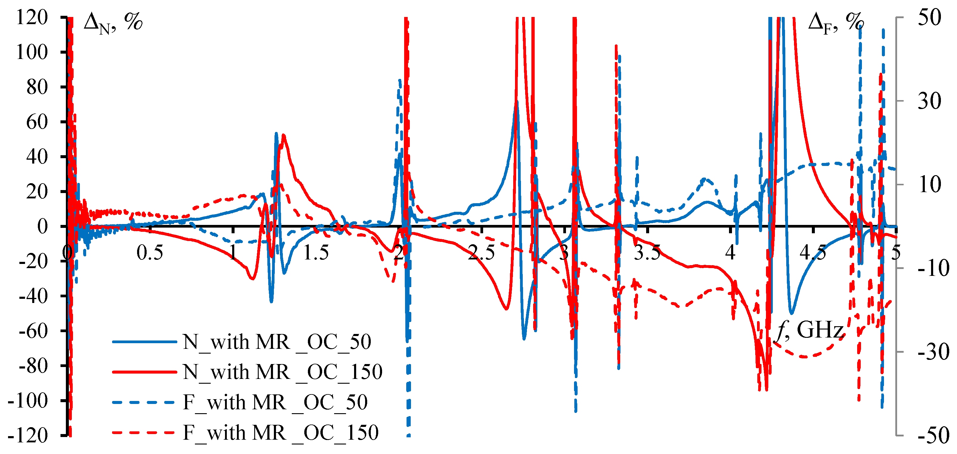
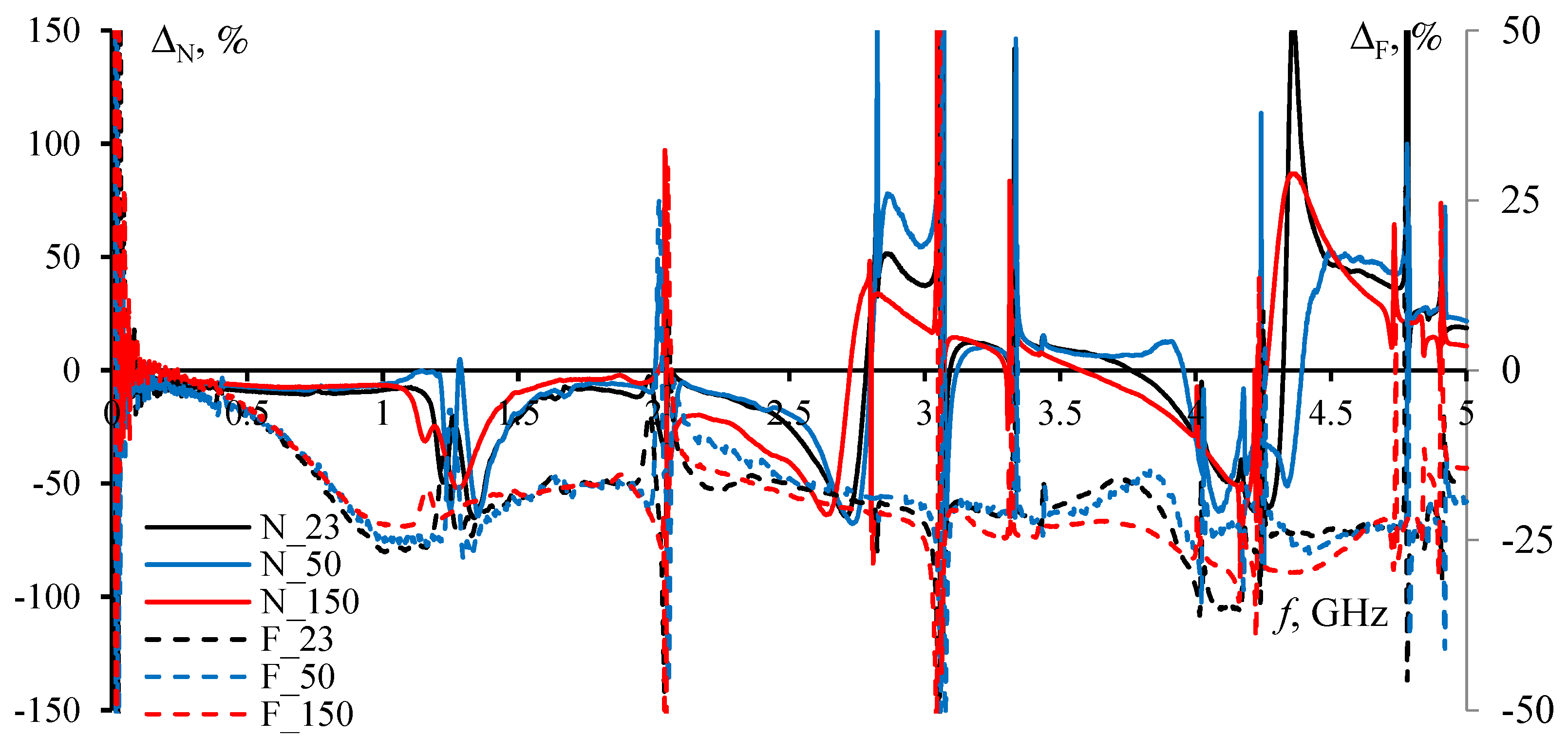
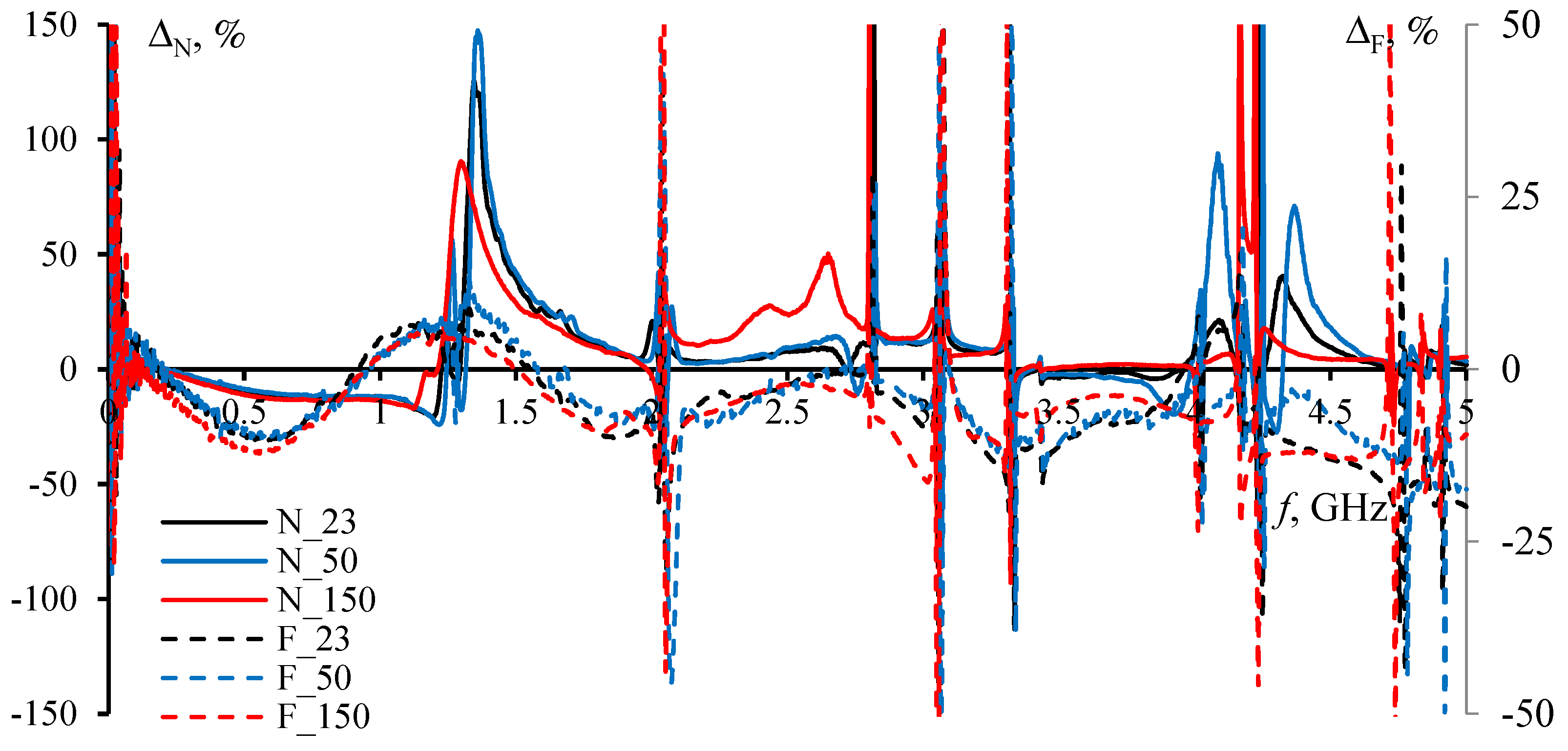
4. Comparative Analysis of REs from PCBs with MR under Climate Impacts

The following are the results of our current research related to the estimation of the REs from structures with MR under climate impacts, which thus far have not been published. In order to estimate the RE from PCBs with MR before and after failures and under various climate impacts, we performed an experimental study in the frequency domain. This study took into account the temperature changes from –50 to 150 °C. Using the VNA R&S ZVA 40 (two ports), we measured the S-parameters of the PCBs having placed their prototypes inside the miniature TEM-cell inside the climate heat–cold chamber (Figure 28). The VNA was used as a meter and generator with 0 dBm output power.
Based on the measured S-parameters for all the PCBs, the level of the voltages and REs from all the PCBs were calculated as follows [68]:
U ( f ) = | S m n ( f ) | P l i n Z l i n ,
E ( f ) = U ( f ) d
where Zlin is the wave impedance of the PCB transmission line, Plin is the power supplied to the input of the PCB transmission line, d is the distance between the TEM-cell central and reference conductors, and m and n are the port numbers. The RE calculations were carried out for the measured frequency dependencies of the S-parameters at the input and output of the CC for all the prototypes using Equations (1) and (2) and taking into account that Plin = 1 mW (0 dBm) and Zlin = 50 Ohm. The results obtained using these formulas are acceptable until higher order waves start to propagate and increase the field non-uniformity (here up to 4.8 GHz [63]).
The calculated frequency dependences of the field intensity for all the PCBs at both the near and far ends of the CC of the TEM-cell in the climate chamber at 23 °C are shown in Figure 29, at −50 °C in Figure 30, and at 150 °C in Figure 31. The differences in the calculated frequency dependences of the field intensity obtained from the measured S-parameters at the near and far ends of the TEM-cell CC in the climate chamber at −50 and 150 °C from those dependences obtained at 23 °C for the PCB without MR are presented in Figure 32, with MR in Figure 33, and with MR after SC and OC failures in Figure 34 and Figure 35, respectively. The average differences in the calculated frequency dependences of the field intensity at the near and far ends of the TEM-cell CC in the climate chamber at −50 and 150 °C from the dependencies obtained at 23 °C for all the PCBs were calculated and are presented in Table 4. The differences in the calculated frequency dependences of the field intensity obtained from the measured S-parameters at the near and far ends of the TEM-cell CC in the climate chamber at the different temperatures for the PCB with MR and for the PCB without MR are compared in Figure 36, and for the PCB with MR after SC failure in Figure 37, and for the PCB with MR after OC failure in Figure 38. The average differences in the calculated frequency dependences of field intensity for the PCB with MR obtained for the other PCBs at the near and far ends of the TEM-cell CC in the climate chamber at the different temperatures were calculated and are presented in Table 5. The notation (−) in the results summarized in Table 4 and Table 5 is used to determine if the value is lower or higher than the other one. These differences are calculated as Δ = (E2(f) − E1(f))/E1(f) % where E1(f) and E2(f) are the electrical field intensity magnitudes compared at each frequency, and the average values are calculated as Δavg = ∑((E2(f) − E1(f))/E1(f) %)/N where N = 2001 and is the number of points in the frequency range.
From Figure 29, Figure 30 and Figure 31 it follows that when the frequency increased, the level of RE from the PCB without MR, in general, decreased if the temperature increased on average by 25%. However, the RE level increased when the temperature decreased in the whole frequency range on average by 15%, except at the resonance frequencies (for example, around 1.2, 2.6 and 4.1 GHz at the near end). In addition, there was a shift in the resonances by 50 MHz towards the high frequencies with the temperature decrease, and also by 50 MHz towards the low frequencies with the temperature increase. This happens because of the changes in the substrate dielectric permittivity and the geometric parameters of the transmission line. Note that the material of the boards was flexible, which leads to the appearance of small gaps between the TEM-cell surface and the board plane. Therefore, the spikes caused by these gaps in the measured values during the experiment observed in all figures can be not reasonably considered (for example, at the frequencies of 2 and 3.3 GHz in Figure 29).
It follows from Figure 29, Figure 30, Figure 31, Figure 32 and Figure 33 that at the near-end of the TEM-cell CC for the PCB without MR at the temperature of 150 °C, the RE levels decreased in the frequency ranges of 0.5–1.25, 1.75–2, 2.25–2.75, and 3.25–4.25 GHz, and increased in other frequency ranges. At −50 °C, the RE levels decreased in the resonance frequency areas, for example, in the frequency ranges of 1.2–1.6, 2.7–3, and 4.4–4.7 GHz and increased in the others. At the far end of the TEM-cell CC, there was an increase in RE levels at the low frequencies up to 1.5 GHz and a decrease up to 5 GHz, except at the resonance frequencies at 150 °C. At a temperature of −50 °C, the opposite was observed. The same phenomena were observed for the PCB with MR, but the level of decrease/increase was, on average, 5% higher than the PCB without MR.
The 50 MHz resonance shift also remained with the temperature change, and this shift was directed towards the lower frequencies from the results obtained for the PCB without MR. The sensitivity of the PCB to the temperature change also changes, as can be seen in Figure 32 and Figure 33 where the difference in the measured frequency dependences of field intensities at −50°C and 150°C for the PCB with MR was higher than those for the PCB without MR. However, the magnitudes, on average, were 20% less than those for the PCB without MR, especially at the far end, as shown in Figure 29, Figure 30, Figure 31 and Figure 36.
It follows from Figure 29, Figure 30 and Figure 31 that the resonance shifts were the same for both the PCB with MR and without it. The behavior of the frequency dependences of voltages at −50 and 150 °C was also preserved, but the sensitivity of the PCB after SC failure to the temperature change increased by about 10%, as can be seen from Figure 33 and Figure 34. The magnitudes were, on average, 10% less than for the PCB with MR, especially at the far end of the whole frequency range, except at the resonance frequencies, as can be seen in Figure 29, Figure 30, Figure 31 and Figure 37.
It follows from Figure 29, Figure 30 and Figure 31 that the resonance shift for the PCB with MR after the OC failure did not change. The behavior of the frequency dependences of magnitudes at −50 and 150 °C were also preserved, but the sensitivity of the PCB after OC failure to the temperature change was lower by 10%, as illustrated in Figure 33 and Figure 35. The magnitudes were on average greater by 10% than those for the PCB with MR, especially at the far end of the whole frequency range, except at the resonance frequencies, as shown in Figure 29, Figure 30, Figure 31 and Figure 38.
In summary, four PCB prototypes were manufactured to estimate the REs from structures without MR and with it before and after short and open circuit failures. The voltage magnitudes and the levels of RE were obtained for all PCBs based on their S-parameters measured under different temperatures. It was found that with the frequency growth, the level of REs from the PCB without MR, in general, decreased with increasing temperature on average by 25%, and increased with temperature decrease in the whole frequency range on average by 15%, except at the resonance frequencies. Furthermore, there was a noticeable resonance shift by 50 MHz towards the high frequencies with a temperature decrease, and by 50 MHz towards the low frequencies with a temperature increase.
For the PCB with MR after failures, the shift in resonances did not change. The behavior of frequency dependences of the magnitudes at −50 and 150 °C was also preserved, but the sensitivity of PCBs after failures to the temperature change increased by 10% in the case of SC failure, and decreased in the case of OC. The magnitudes were on average lower by 10% in the case of SC than those for the PCB with MR, and higher in the case of OC, especially at the far end of the whole studied frequency range, except at the resonance frequencies.
When the temperature changes, the dielectric permittivity of the PCB material changes and the resonance frequencies shift. The value and sign of this change are determined by the thermal coefficient of material. The material used in the work has a big and positive thermal coefficient. However, one can use another material with a lower or even a negative thermal coefficient, which allows one to considerably decrease the sensitivity of the required characteristics to the temperature change.
In future, we are planning to investigate the change in the RE from PCBs with double and triple MR under climate impacts and even after failure. Moreover, we are working on developing new models for estimating the REs from such structures. These models take into account the losses in the conductors and dielectric, the frequency and temperature dependencies of the relative dielectric permittivity, and the dissipation factor of different materials. All this will be used to enhance the capability of our domestic software (TALGAT 2021, TUSUR-university, Tomsk, Russia), which has been designed to solve various electromagnetic problems (compatibility, radiation, scattering, and shielding). The ongoing research on MR methods, especially in terms of REs, will lead us to develop new methods for manufacturing and tracing circuits with MR taking into account the level of REs from them, and even their susceptibility to it.

5. Conclusions

MR, in fact, employs the excess bandwidth of the transmission lines passband, when its upper frequency is much higher than the upper frequency of the useful signal spectrum. Then, a reconstruction of the like-named single lines of several identical circuits into coupled (single reservation) or multiconductor (multiple reservation) transmission lines is performed by manufacturing conductors of the lines in a unified structure with considerable electromagnetic coupling between them. As a result, the upper frequency passband is reduced to the upper frequency of the useful signal spectrum. Thus, the propagation of the useful signal is not disturbed. However, the transmission lines obtain new properties that can be used to attenuate the unwanted signals. Accordingly, at frequencies above the upper frequency of the useful signal spectrum, minimums appear in the frequency dependence of the transmission coefficient magnitudes. Under the conducted excitation of a USP with a dangerous amplitude at the input of any of the lines, this pulse is decomposed into pulses of lower amplitude at the line output. As a result, each conductor of the reserved circuit, together with a single reference conductor, becomes an EMI filter. This is achieved without adding any components, but rather using the existing conductors and modifying their placement in the whole structure. Such structures are reciprocal or near to that, which allows to attenuate not only the externally conducted excitations, but also conducted emissions from the components of the reserved circuits. In addition, the radiated emissions from such lines can be also attenuated, reducing the shielding requirements.
All this concerns the operation of a reserved circuit before failure, so that these advantages can be used for a long time until the reserved circuit fails. Once the reserved circuit fails and a switching to the reserving circuit has been performed, these advantages may change, but only insignificantly and only in the circuit part with the failure, while in the other parts they will remain the same. In the case of multiple reservation, it is possible to select a more preferable reserving circuit among the remaining ones to switch to. Note that in the case of single reservation, the amplitude of the exciting pulse can be reduced by a factor of two, and in the case of triple reservation by a factor of four, which is achieved due to the mirror symmetry in one and two planes, respectively. This can be achieved even with weak electromagnetic coupling, whereas with strong coupling, these values can increase by several times. Moreover, for stronger coupling the time intervals between the pulses also increase, which prevents their partial overlapping.
Thus, modal reservation provides a unique opportunity to not only increase the reliability of critical radioelectronic equipment by means of the reserving circuits, but, thanks to them, also consistently ensure its electromagnetic compatibility (both before and after failure and under any climate impacts). The latter is provided by attenuating the conducted and radiated emissions from such equipment, as well as weakening the impacts on it, particularly, those induced by intentional USPs generated by electromagnetic weapons.

Author Contributions

Conceptualization, A.A.H. and T.R.G.; methodology, T.R.G. and A.A.H.; software, A.A.H.; validation, A.A.H.; formal analysis, A.A.H. and T.R.G.; investigation, A.A.H.; resources, T.R.G.; writing—original draft preparation, A.A.H.; writing—review and editing, T.R.G.; visualization, A.A.H.; supervision, T.R.G.; project administration, A.A.H. All authors have read and agreed to the published version of the manuscript.

Funding

This research was funded by the Russian Science Foundation (project 19-19-00424, ”https://rscf.ru/project/19-19-00424/ (accessed on 1 October 2022)”, prototypes modeling) and by the Ministry of Science and Higher Education and Science of the Russian Federation project (project FEWM-2022-0001, review and experiment) in TUSUR.

Conflicts of Interest

The authors declare no conflict of interest.

Abbreviations

CCCentral conductor
EMCElectromagnetic compatibility
EMIElectromagnetic interference
MRModal reservation
OCOpen circuit
PCBPrinted circuit board
RERadiated emissions
SCShort circuit
USPUltrashort pulses
VNAVector network analyzer

References

  1. Trivedi, K.; Bobbio, A. Reliability and Availability Engineering: Modeling, Analysis, and Applications; Cambridge University Press: Cambridge, UK, 2017. [Google Scholar]
  2. Amari, S.V.; Dill, G. Redundancy optimization problem with warm-standby redundancy. In Proceedings of the Annual Reliability and Maintainability Symposium (RAMS), San Jose, CA, USA, 25–28 January 2010; pp. 1–6. [Google Scholar]
  3. Kuo, S.V.W.; Prasad, V.R.; Tillman, F.A.; Hwang, C.L. Optimal Reliability Design: Fundamentals and Applications; Cambridge University Press: Cambridge, UK, 2001. [Google Scholar]
  4. Von Neumann, J. Probabilistic logics and the synthesis of reliable organisms from unreliable components. In Automata Studies; Shannon, C.E., McCarthy, J., Eds.; Princeton Univ. Press: Princeton, NJ, USA, 1956; pp. 43–98. [Google Scholar]
  5. Chen, D.M. Satellite Engineering Series: Communications Satellite Payload Technology; China Astronautic Publishing House: Beijing, China, 2001. [Google Scholar]
  6. Coit, D.W. Maximization of System Reliability with a Choice of Redundancy Strategies. IIE Trans. 2003, 35, 535–543. [Google Scholar] [CrossRef]
  7. Grida, M.; Zaid, A.; Kholief, G. Repairable 3-out-of-4: Cold standby system availability. In Proceedings of the Annual Reliability and Maintainability Symposium (RAMS), Orlando, FL, USA, 23–26 January 2017; pp. 1–6. [Google Scholar]
  8. Lobur, M.; Stefanovych, T.; Shcherbovskykh, S. Modelling of type I and II errors of switching device for systems with hot and cold redundancy based on two-terminal dynamic fault tree. In Proceedings of the 14th International Conference of the Experience of Designing and Application of CAD Systems in Microelectronics (CADSM), Lviv, Ukraine, 21–25 February 2017; pp. 19–21. [Google Scholar]
  9. Li, Y.; Zhang, Y.; Cao, R.; Liu, X.; Lv, C.; Liu, J. Redundancy design of modular DC solid-state transformer based on reliability and efficiency evaluation. CPSS Trans. Power Electron. Appl. 2021, 6, 115–126. [Google Scholar] [CrossRef]
  10. Sankaraiah, G.; Raghunatha Reddy, Y.; Umasankar, C.; Sarma, B.D. Design and optimization of an Integrated Reliability redundancy system with multiple constraints. In Proceedings of the 2nd International Conference on Reliability, Safety and Hazard—Risk-Based Technologies and Physics-of-Failure Methods (ICRESH), Mumbai, India, 14–16 December 2010; pp. 118–122. [Google Scholar]
  11. Pan, D. Study on Optimization of System Reliability Redundancy Based on Hybrid Intelligent Algorithm. In Proceedings of the International Conference on Environmental Science and Information Application Technology, Wuhan, China, 4–5 July 2009; pp. 560–563. [Google Scholar]
  12. Boland, P.J.; El-Neweihi, E. Component redundancy vs system redundancy in the hazard rate ordering. IEEE Trans. Reliab. 1995, 44, 614–619. [Google Scholar] [CrossRef]
  13. Shcherbovskykh, S.; Stefanovych, T. Modelling features of type I and II errors of switching device for system with double hot and double cold redundancy based on two-terminal dynamic fault tree. In Proceedings of the 14th International Conference on Advanced Trends in Radioelecrtronics, Telecommunications and Computer Engineering (TCSET), Lviv, Ukraine, 20–24 February 2018; pp. 753–756. [Google Scholar]
  14. Neves, F.G.R.; Saotome, O. Comparison between Redundancy Techniques for Real Time Applications. In Proceedings of the Fifth International Conference on Information Technology: New Generations (ITNG), Las Vegas, NV, USA, 7–9 April 2008; pp. 1299–1300. [Google Scholar]
  15. Peterson, W.; Weldon, E. Error-Correcting Codes, 2nd ed.; MIT Press: Cambridge, MA, USA, 1972. [Google Scholar]
  16. Zhu, X.; Xu, H.; Long, H.; Li, Q.; Li, Z.; Liu, H.; Wang, Y. Memristive Stateful Logic with N-Modular Redundancy Error Correction Design towards High Reliability. In Proceedings of the 5th IEEE Electron Devices Technology & Manufacturing Conference (EDTM), Chengdu, China, 8–11 April 2021; pp. 1–3. [Google Scholar]
  17. Sun, Z.; Ambrosi, E.; Bricalli, A.; Ielmini, D. Logic Computing with Stateful Neural Networks of Resistive Switches. Adv. Mater. 2018, 30, 1802554. [Google Scholar] [CrossRef] [Green Version]
  18. Hansen, P.; Linton, M.; Mayo, R.; Murphy, M.; Patterson, D. Introduction to the iAPX 482 architecture. ACM SIGARCH Comput. Archit. News 1982, 10, 17–26. [Google Scholar] [CrossRef]
  19. Namazi, A.; Nourani, M. Gate-Level Redundancy: A New Design-for-Reliability Paradigm for Nanotechnologies. IEEE Trans. Very Large-Scale Integr. (VLSI) Syst. 2010, 18, 775–786. [Google Scholar] [CrossRef]
  20. Xiong, X.; Zhao, H.T.; Hu, T.B. Research on Redundancy Solution of Satellite Transponders Based on Reliability Analysis. In Proceedings of the International Conference on Quality, Reliability, Risk, Maintenance, and Safety Engineering (QR2MSE), Zhangjiajie, China, 6–9 August 2019; pp. 689–694. [Google Scholar]
  21. Sklaroff, J.R. Redundancy Management Technique for Space Shuttle Computers. IBM J. Res. Dev. 1976, 20, 20–28. [Google Scholar] [CrossRef]
  22. Xiao, C.; Deng, L. Reliability Research on Airborne Dual Redundancy of Electrical Wiring Interconnection System. In Proceedings of the 11th International Symposium on Computational Intelligence and Design (ISCID), Hangzhou, China, 8–9 December 2018; pp. 137–140. [Google Scholar]
  23. Zhang, D.; Zhao, M.; Cheng, E.; Chen, Y. GPR-Based EMI Prediction for UAV’s Dynamic Datalink. IEEE Trans. Electromagn. Compat. 2021, 63, 19–29. [Google Scholar] [CrossRef]
  24. Rentschler, M.; Laukemann, P. Performance analysis of parallel redundant WLAN. In Proceedings of the IEEE 17th International Conference on Emerging Technologies & Factory Automation (ETFA), Krakow, Poland, 17–21 September 2012; pp. 1–8. [Google Scholar]
  25. Slee, D.; Stepan, J.; Wei, W.; Swart, J. Introduction to printed circuit board failures. In Proceedings of the IEEE Symposium on Product Compliance Engineering, Toronto, ON, Canada, 26–28 October 2009; pp. 1–8. [Google Scholar]
  26. Labib, M.G.; Mahmoud, D.G.; Alkady, G.I.; Adly, I.; Amer, H.H.; Daoud, R.M.; ElSayed, H.M. Heterogeneous Redundancy for PCB Track Failures: An Automotive Example. In Proceedings of the 14th International Conference on Computer Engineering and Systems (ICCES), Cairo, Egypt, 17 December 2019; pp. 189–194. [Google Scholar]
  27. Chen, H.C.; Bai, Y.W. Improvement of High-Current Density PCB Design With PSU Load Balance and Redundancy on a High End Server System. Can. J. Electr. Comput. Eng. 2014, 37, 203–211. [Google Scholar] [CrossRef]
  28. Van Waes, J.; Vankeirsbilck, J.; Pissoort, D.; Boydens, J. Functional safety standard’s techniques and measures in light of electromagnetic interference. In Proceedings of the XXVI International Scientific Conference Electronics (ET), Sozopol, Bulgaria, 13–15 September 2017; pp. 1–4. [Google Scholar]
  29. Pissoort, D.; Armstrong, K. Why is the IEEE developing a standard on managing risks due to EM disturbances? In Proceedings of the IEEE International Symposium on Electromagnetic Compatibility (EMC), Ottawa, ON, Canada, 25–29 July 2016; pp. 78–83. [Google Scholar]
  30. Van Waes, J.; Vanoost, D.; Vankeirsbilck, J.; Lannoo, J.; Pissoort, D.; Boydens, J. Resilience of Error Correction Codes Against Harsh Electromagnetic Disturbances: Fault Mechanisms. IEEE Trans. Electromagn. Compat. 2020, 62, 1017–1027. [Google Scholar] [CrossRef]
  31. Luo, S.; Batarseh, I. A review of distributed power systems. Part II. High frequency AC distributed power systems. IEEE Aerosp. Electron. Syst. Mag. 2006, 21, 5–14. [Google Scholar] [CrossRef]
  32. Pissoort, D.; Lannoo, J.; van Waes, J.; Degraeve, A.; Boydens, J. Techniques and measures to achieve EMI resilience in mission- or safety-critical systems. IEEE Electromagn. Compat. Mag. 2017, 6, 107–114. [Google Scholar] [CrossRef]
  33. Lannoo, J.; Degraeve, A.; Vanoost, D.; Boydens, J.; Pissoort, D. Study on the use of different transmission line termination strategies to obtain EMI-diverse redundant systems. In Proceedings of the IEEE International Symposium on Electromagnetic Compatibility and 2018 IEEE Asia-Pacific Symposium on Electromagnetic Compatibility (EMC/APEMC), Suntec City, Singapore, 14–18 May 2018; pp. 210–215. [Google Scholar]
  34. Mora, N.; Vega, F.; Lugrin, G.; Rachidi, F.; Rubinstein, M. Study and Classification of Potential IEMI Sources. Syst. Des. Assess. Notes 2014, 41, 1–92. [Google Scholar]
  35. Gazizov, T.R.; Zabolotsky, A.M. New approach to EMC protection. In Proceedings of the 18th International Zurich Symposium on Electromagnetic Compatibility, Munich, Germany, 24–28 September 2007; pp. 273–276. [Google Scholar]
  36. Orlov, P.; Gazizov, T. Contactless Modal Phenomena Based Approach to Detecting, Identifying, and Diagnosing of Electrical Connections. Complexity 2018, 2018, 5081684. [Google Scholar] [CrossRef] [Green Version]
  37. Orlov, P.E.; Medvedev, A.V.; Sharafutdinov, V.R.; Kalimulin, I.F. Quasistatic simulation of ultrashort pulse propagation in the spacecraft autonomous navigation system circuit with modal reservation. In Proceedings of the International Multi-Conference on Engineering, Computer and Information Sciences (SIBIRCON), Novosibirsk, Russia, 18–22 September 2017; pp. 495–500. [Google Scholar]
  38. Orlov, P.E.; Medvedev, A.V.; Sharafutdinov, V.R. Quasistatic Simulation of Ultrashort Pulse Propagation in the Spacecraft Autonomous Navigation System Power Circuit with Modal Reservation. In Proceedings of the 19th International Conference of Young Specialists on Micro/Nanotechnologies and Electron Devices (EDM), Erlagol, Russia, 29 June–3 July 2018; pp. 1–6. [Google Scholar]
  39. Orlov, P.E.; Buichkin, E.N.; Belousov, A.O.; Gazizov, T.R. Method of lay-out of a multilayer PCB for circuits with triple reservation. In Proceedings of the International Siberian Conference on Control and Communications (SIBCON), Astana, Kazakhstan, 29–30 June 2017; pp. 1–4. [Google Scholar]
  40. Belousov, A.O.; Chernikova, E.B.; Samoylichenko, M.A.; Medvedev, A.V.; Nosov, A.V.; Gazizov, T.R.; Zabolotsky, A.M. From Symmetry to Asymmetry: The Use of Additional Pulses to Improve Protection against Ultrashort Pulses Based on Modal Filtration. Symmetry 2020, 12, 1117. [Google Scholar] [CrossRef]
  41. Orlov, P.E.; Buichkin, E.N. Quasistatic and electromagnetic simulation of interconnects of printed circuit boards with modal reservation. In Proceedings of the 18th International Conference of Young Specialists on Micro/Nanotechnologies and Electron Devices (EDM), Erlagol, Russia, 29 June–July 2017; pp. 54–58. [Google Scholar]
  42. Hasan, A.A.; Kvasnikov, A.A.; Gazizov, T.R. Approach to Estimation of Radiated Emission from Circuits with Modal Reservation. In Proceedings of the 21st International Conference of Young Specialists on Micro/Nanotechnologies and Electron Devices (EDM), Chemal, Russia, 29 June–July 2020; pp. 169–173. [Google Scholar]
  43. Hasan, A.A.; Gazizov, T.R. Estimation of the Radiated Emission from a Single and Coupled Wires with Insulation above the Ground Plane. In Proceedings of the IEEE 22nd International Conference of Young Professionals in Electron Devices and Materials (EDM), Souzga, the Altai Republic, Russia, 30 June–4 July 2021; pp. 149–152. [Google Scholar]
  44. Alhaj Hasan, A.; Zhechev, Y.S.; Gazizov, T.R. Estimation of radiated emissions from a structure with a single modal reservation. J. Phys. Conf. Ser. 2021, 1862, 012003. [Google Scholar] [CrossRef]
  45. Hasan, A.A.; Gazizov, T.R. Comparing the Estimates of the Radiated Emission from a Structure with Modal Reservation by Two Approaches. In Proceedings of the IEEE 22nd International Conference of Young Professionals in Electron Devices and Materials (EDM), Souzga, the Altai Republic, Russia, 30 June–4 July 2021; pp. 145–148. [Google Scholar]
  46. Orlov, P.E.; Medvedev, A.V.; Sharafutdinov, V.R.; Gazizov, T.R.; Ubaichin, A.V. Methods for increasing noise immunity of radio electronic systems with redundancy. J. Phys. Conf. Ser. 2018, 1015, 052022. [Google Scholar] [CrossRef]
  47. Sharafutdinov, V.R.; Medvedev, A.V. Using Modal Reservation for Ultrashort Pulse Attenuation after Failure. In Proceedings of the International Multi-Conference on Engineering, Computer and Information Sciences (SIBIRCON), Novosibirsk, Russia, 21–27 October 2019; pp. 0293–0296. [Google Scholar]
  48. Medvedev, A.V.; Gazizov, T.R.; Zhechev, Y.S. Evaluating modal reservation efficiency before and after failure. J. Phys. Conf. Ser. 2020, 1488, 012015. [Google Scholar] [CrossRef] [Green Version]
  49. Medvedev, A.V.; Zhechev, Y.S. Analysis of frequency characteristics of a structure with single modal reservation before and after failure. J. Phys. Conf. Ser. 2020, 862, 022037. [Google Scholar] [CrossRef]
  50. Medvedev, A.V.; Zhechev, Y.S.; Gazizov, T.R. Experimental Study of a Structure with Single Modal Reservation before and after Failure. IEEE Trans. Electromagn. Compat. 2022, 64, 1171–1181. [Google Scholar] [CrossRef]
  51. Medvedev, A.V. Studying the switching order for a three-wire structure with modal reservation after failures. J. Phys. Conf. Ser. 2020, 919, 052022. [Google Scholar] [CrossRef]
  52. Belousov, A.O.; Medvedev, A.V.; Chernikova, E.B.; Gazizov, T.R.; Zabolotsky, A.M. Switching Order after Failures in Symmetric Protective Electrical Circuits with Triple Modal Reservation. Symmetry 2021, 13, 1074. [Google Scholar] [CrossRef]
  53. Gazizov, R.R.; Medvedev, A.V.; Gazizov, T.R. Using Portraits of N-Norms for Large-Scale Investigation of Circuits with Modal Reservation. In Proceedings of the Dynamics of Systems, Mechanisms and Machines (Dynamics), Omsk, Russia, 9–11 November 2021; pp. 1–4. [Google Scholar]
  54. Zhechev, Y.S.; Zhecheva, A.V.; Kvasnikov, A.A.; Zabolotsky, A.M. Using N-norms for analyzing symmetric protective electrical circuits with triple modal reservation. Symmetry 2021, 13, 2390. [Google Scholar] [CrossRef]
  55. Mora, N.; Vega, F.; Lugrin, G.; Rachidi, F.; Rubinstein, M. System Design and Assessment Notes 41. 2014. [Google Scholar]
  56. Harrington, R.F. Matrix methods for field problems. Proc. IEEE 1967, 55, 136–149. [Google Scholar] [CrossRef] [Green Version]
  57. Official Website of Elmika Company LLC. STF Technical Characteristics. Available online: http://elmica.ru/assets/files/listovki/folgirovannyj-steklotekstolit-2016.pdf (accessed on 30 September 2022).
  58. Kuksenko, S.P. Preliminary results of TUSUR University project for design of spacecraft power distribution network: EMC simulation. IOP Conf. Ser. Mater. Sci. Eng. 2019, 560, 012110. [Google Scholar] [CrossRef] [Green Version]
  59. Alhaj Hasan, A.; Gazizov, T.R. Studying the Features of a PCB with Modal Reservation in the Frequency Domain Using TALGAT. In Proceedings of the IEEE Ural-Siberian Conference on Biomedical Engineering, Radioelectronics and Information Technology (USBEREIT), Yekaterinburg, Russia, 19–21 September 2022; pp. 102–107. [Google Scholar]
  60. Alhaj Hasan, A.; Gazizov, T.R. Frequency Characteristics of PCB with Modal Reservation before and after Failure Using TALGAT. In Proceedings of the IEEE 23rd International Conference of Young Professionals in Electron Devices and Materials (EDM), Altai, Russia, 30 June–4 July 2022; pp. 140–146. [Google Scholar]
  61. Komnatnov, M.E.; Gazizov, T.R. TEM Chamber. Patent No. 2,606,173, 28 December 2015. [Google Scholar]
  62. Demakov, V.; Komnatnov, M.E. Improved TEM-cell for EMC tests of integrated circuits. In Proceedings of the IEEE International Multi-Conference on Engineering, Computer and Information Sciences (SIBIRCON), Novosibirsk, Russia, 18–22 September 2017; pp. 399–402. [Google Scholar]
  63. Alhaj Hasan, A.; Gazizov, T.R. Measuring the Level of Radiated Emissions from PCBs with Modal Reservation before and after Failure. In Proceedings of the IEEE 23rd International Conference on Actual Problems of Electron Devices Engineering (APEDE), Saratov, Russia, 22–23 September 2022; pp. 13–16. [Google Scholar]
  64. Alhaj Hasan, A.; Gazizov, T.R. TEM-cell Measurements of the Radiated Emissions from PCBs with Modal Reservation before and after Failure. In Proceedings of the IEEE The International Ural Conference on Electrical Power Engineering (UralCon), Magnitogorsk, Russia, 23–25 September 2022; pp. 196–200. [Google Scholar]
  65. Alhaj Hasan, A.; Gazizov, T.R. Measuring Frequency Characteristic of PCBs with Modal Reservation under Climatic Impact. In Proceedings of the IEEE 2nd International Conference Problems of Informatics, Electronics and Radio Engineering (PIERE), Novosibirsk, Russia, 11–13 November 2022. [Google Scholar]
  66. Alhaj Hasan, A.; Gazizov, T.R. Measuring Frequency Characteristic of PCBs with Modal Reservation under Climatic Impact before and after Short Circuit Failure. In Proceedings of the IEEE 23rd International Conference on Dynamics of systems, mechanisms and machines, Omsk, Russia, 15–17 November 2022. [Google Scholar]
  67. Alhaj Hasan, A.; Gazizov, T.R. Measuring Frequency Characteristics of PCBs with Modal Reservation before and after Open Circuit Failure under Climatic Impact. In Proceedings of the IEEE International Conference of Siberian Conference on Control and Communications (Sibcon), Tomsk, Russia, 17–19 November 2022. [Google Scholar]
  68. Crawford, M.L. Generation of Standard EM Fields Using TEM Transmission Cells. IEEE Trans. Electromagn. Compat. 1974, 16, 189–195. [Google Scholar] [CrossRef]
Figure 1. The structural cross-section for the method of routing printed conductors in circuits with modal reservation (No. 1).
Symmetry 14 02466 g001
Figure 2. The structural cross-section for the method of routing printed conductors with additional dielectric in circuits with modal reservation (No. 2).
Symmetry 14 02466 g002
Figure 3. The structural cross-section for the method of modal reservation of PCBs (No. 3).
Symmetry 14 02466 g003
Figure 4. The structural cross-section for the method of tracing a double-sided PCB for circuits with modal reservation (No. 4).
Symmetry 14 02466 g004
Figure 5. The structural cross-section for the method of single modal reservation of meander turns (No. 5).
Symmetry 14 02466 g005
Figure 6. The structural cross-section for the method of routing printed conductors with additional dielectrics for the circuits with double modal reservation (No. 6).
Symmetry 14 02466 g006
Figure 7. The structural cross-section for the method of routing printed conductors on a two-layered printed circuit board for circuits with reservation of the outside (a) and inside (b) signal layers (No. 7).
Symmetry 14 02466 g007
Figure 8. The structural cross-section for the method of routing printed power conductors of circuits with modal reservation (No. 8).
Symmetry 14 02466 g008
Figure 9. The structural cross-section for the method of arranging the outer components on PCBs with modal reservation (No. 9).
Symmetry 14 02466 g009
Figure 10. The schematic representation of the component molding and the mutual arrangement of the pins without (a) and with (b) using the method proposed in (No. 10).
Symmetry 14 02466 g010
Figure 11. The structural cross-section for the method of assembling non-molded radioelectronic components on PCBs with modal reservation (No. 10).
Symmetry 14 02466 g011
Figure 12. The structural cross-section for the method of arranging the inner components on PCBs with modal reservation (No. 11).
Symmetry 14 02466 g012
Figure 13. The structural cross-section for the method of modal reservation of flat cables (No. 12).
Symmetry 14 02466 g013
Figure 14. The structural cross-section for the method of triple modal reservation in multilayered printed circuit boards (No. 13).
Symmetry 14 02466 g014
Figure 15. The structural cross-section for the method of triple modal reservation of PCB conductors (No. 14).
Symmetry 14 02466 g015
Figure 16. The structural cross-section for the method of arranging printed conductors in circuits with modal reservation (No. 15).
Symmetry 14 02466 g016
Figure 17. The structural cross-section for the method of arranging a multilayer PCB with modal reservation outside (a) and inside (b) the signal layers (No. 16).
Symmetry 14 02466 g017aSymmetry 14 02466 g017b
Figure 18. The structural cross-section for the method of switching circuits with double modal reservation after failure (No. 17).
Symmetry 14 02466 g018
Figure 19. The structural cross-section for the method of switching circuits with triple modal reservation after failure (No. 18).
Symmetry 14 02466 g019
Figure 20. The cross-sectional parameters of the structures without (a) and with (b) MR.
Symmetry 14 02466 g020
Figure 21. The structures without (a) and with (b) MR: equivalent schematic diagrams where R = 50 Ω and E is a harmonic electromotive source with an amplitude of 1 V.
Symmetry 14 02466 g021
Figure 22. The PCB prototypes without (a) and with single (b) MR.
Symmetry 14 02466 g022
Figure 23. The climate heat-cold chamber (a) and the vector network analyzer (b).
Symmetry 14 02466 g023
Figure 24. The structures with single MR after SC (a) and OC (b) failures: equivalent schematic diagrams where R = 50 Ω and E is a harmonic source with an amplitude of 1 V.
Symmetry 14 02466 g024
Figure 25. The PCB prototypes with MR after SC (a) and OC (b) failures.
Symmetry 14 02466 g025
Figure 26. The classical (a) and miniature (b) TEM-cells.
Symmetry 14 02466 g026
Figure 27. The connection of VNA ports to the input and output of the classical (a) and miniature (b) TEM-cell CC (Ports 3 and 4), and to the PCBs (Ports 1 and 2).
Symmetry 14 02466 g027
Figure 28. The TEM-cell inside the climate heat–cold chamber (a), connection of VNA Port 2 to the output of the TEM-cell CC and Port 1 to the PCB port (b).
Symmetry 14 02466 g028
Figure 29. The calculated frequency dependences of the field intensities based on the measured S-parameters for all the PCBs at the both near and far ends of the central conductor of the TEM-cell in the climate chamber at 23 °C.
Symmetry 14 02466 g029
Figure 30. The calculated frequency dependences of the field intensities based on the measured S-parameters for all PCBs at the both near and far ends of the central conductor of the TEM-cell in the climatic chamber at −50 °C.
Symmetry 14 02466 g030
Figure 31. The calculated frequency dependences of the field intensities based on the measured S-parameters for all PCBs at the both near and far ends of the central conductor of the TEM-cell in the climate chamber at 150 °C.
Symmetry 14 02466 g031
Figure 32. The differences in the calculated frequency dependences of the field intensities at the near and far ends of the central conductor of the TEM-cell in the climate chamber at −50 and 150 °C from the temperature of 23 °C for the PCB without MR.
Symmetry 14 02466 g032
Figure 33. The differences in the calculated frequency dependences of the field intensities at the near and far ends of the central conductor of the TEM-cell in the climate chamber at −50 and 150 °C from the temperature of 23 °C for the PCB with MR.
Symmetry 14 02466 g033
Figure 34. The differences in the calculated frequency dependences of the field intensities at the near and far ends of the central conductor of the TEM-cell in the climate chamber at −50 and 150 °C from the temperature of 23 °C for the PCB with MR after SC failure.
Symmetry 14 02466 g034
Figure 35. The differences in the calculated frequency dependences of the field intensities at the near and far ends of the central conductor of the TEM-cell in the climate chamber at −50 and 150 °C from the temperature of 23 °C for the PCB with MR after OC failure.
Symmetry 14 02466 g035
Figure 36. The difference in the calculated frequency dependences of the field intensities for the PCB with MR from those for the PCB without MR at the near and far ends of the central conductor of the TEM-cell in the climate chamber at different temperatures.
Symmetry 14 02466 g036
Figure 37. The difference in the calculated frequency dependences of the field intensities for the PCB with MR after the SC failure from those before the failure at the near and far ends of the central conductor of the TEM-cell in the climate chamber at different temperatures.
Symmetry 14 02466 g037
Figure 38. The difference in the calculated frequency dependences of the field intensities for the PCB with MR after the OC failure from those before failure at the near and far ends of the central conductor of the TEM-cell in the climate chamber at different temperatures.
Symmetry 14 02466 g038
Table 1. General comparation of MR with other EMI protection methods.
No.MethodReliabilityEMCStability after FailureCost Ease of Implementation
1Cold redundancy++++
2Hot redundancy++
3EMI-filters+
4MR++++
(+) good and (−) poor.
Table 2. All the obtained patents on MR organized by the order mentioned in the text.
No.RF Patent No.Date of PublicationTitle
1260385010 December 2016Method of routing printed conductors in circuits with MR
2260385110 December 2016Method of routing printed conductors with additional dielectricin circuits with MR
3260384310 December 2016Method of modal reservation of PCBs
4276233620 December 2021Method of tracing a double-sided PCB for circuits with MR
5273260725 September 2020Method of single MR of meander turns
6275223223 July 2021Method of routing printed conductors with additional dielectricin circuits with double MR
7275223323 July 2021Method of routing printed conductors on two-layered PCBs outside and inside the signal layers for circuits with reservation
827795368 September 2022Method of routing printed power conductors in circuits with MR
9261415623 March 2017Method of arranging the outer components on PCBs with MR
1026938385 July 2019Method of assembling non-molded radioelectronic components on PCBs with MR
1126246375 July 2017Method of arranging the inner components on the PCBs with MR
12260384810 December 2016Method of modal reservation in flat cables
1326632302 August 2018Method of triple MR in multilayered PCBs
14273895521 December 2020Method of triple MR of PCB conductors
15275167215 July 2021Method of arranging printed conductors in circuits with MR
16275407826 August 2021Method of arranging multilayer PCBs with MR outside and inside the signal layers
17277051618 April 2022Method of switching circuits with double MR after failures
18276719016 March 2022Method of switching circuits with triple MR after failures
Table 3. Summary of the research on RE from PCBs with MR.
No.ReferenceResearchNotes
1[42]New algorithm able to give accurate results with less computational costs to obtain the far field electric intensity from a test structure with MRComparison of the results of the proposed algorithm with those obtained using the electrodynamic approach (MoM) showed good consistency
2[43]Testing the proposed algorithm on wires with dielectric insulationWhen increasing the dielectric permittivity, the wave impedance of a single wire decreased and the current amplitudes increased when compared to values from a wire without insulation
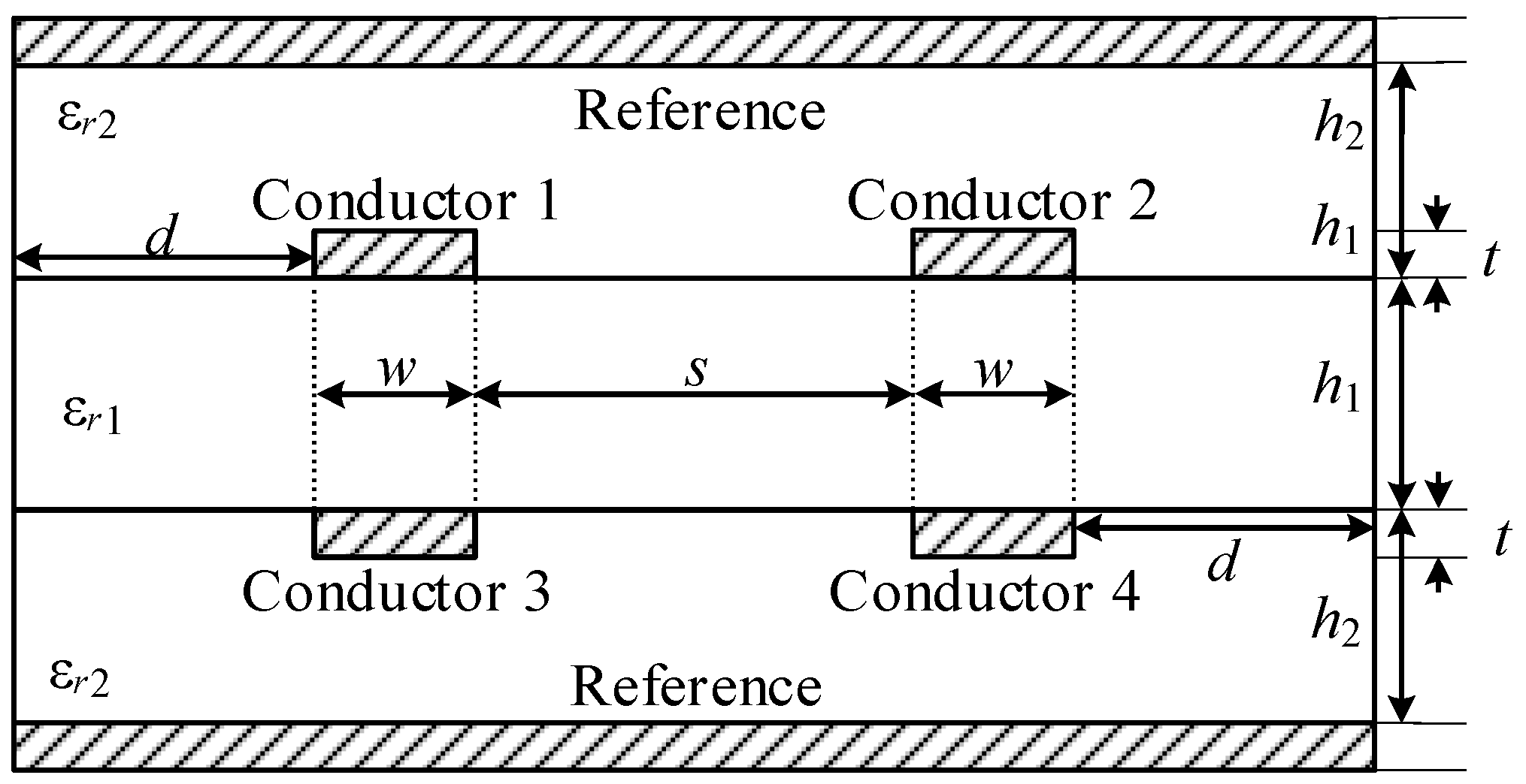
3[44]Obtaining the RE from MR-based PCBs using the electrodynamic approach (FDTD)Using MR reduced RE from PCBs
4[45]Analysis of the MR implementation effect on PCB RE and comparing the results of the proposed algorithm with those obtained using FDTDMR application reduced RE from PCBs, proven by two different approaches
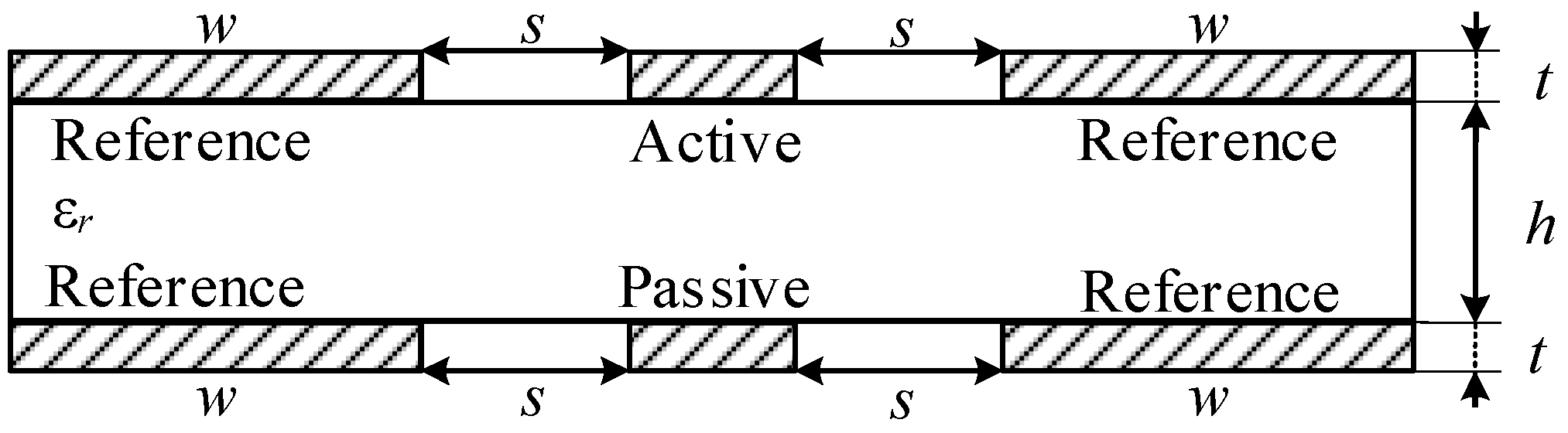
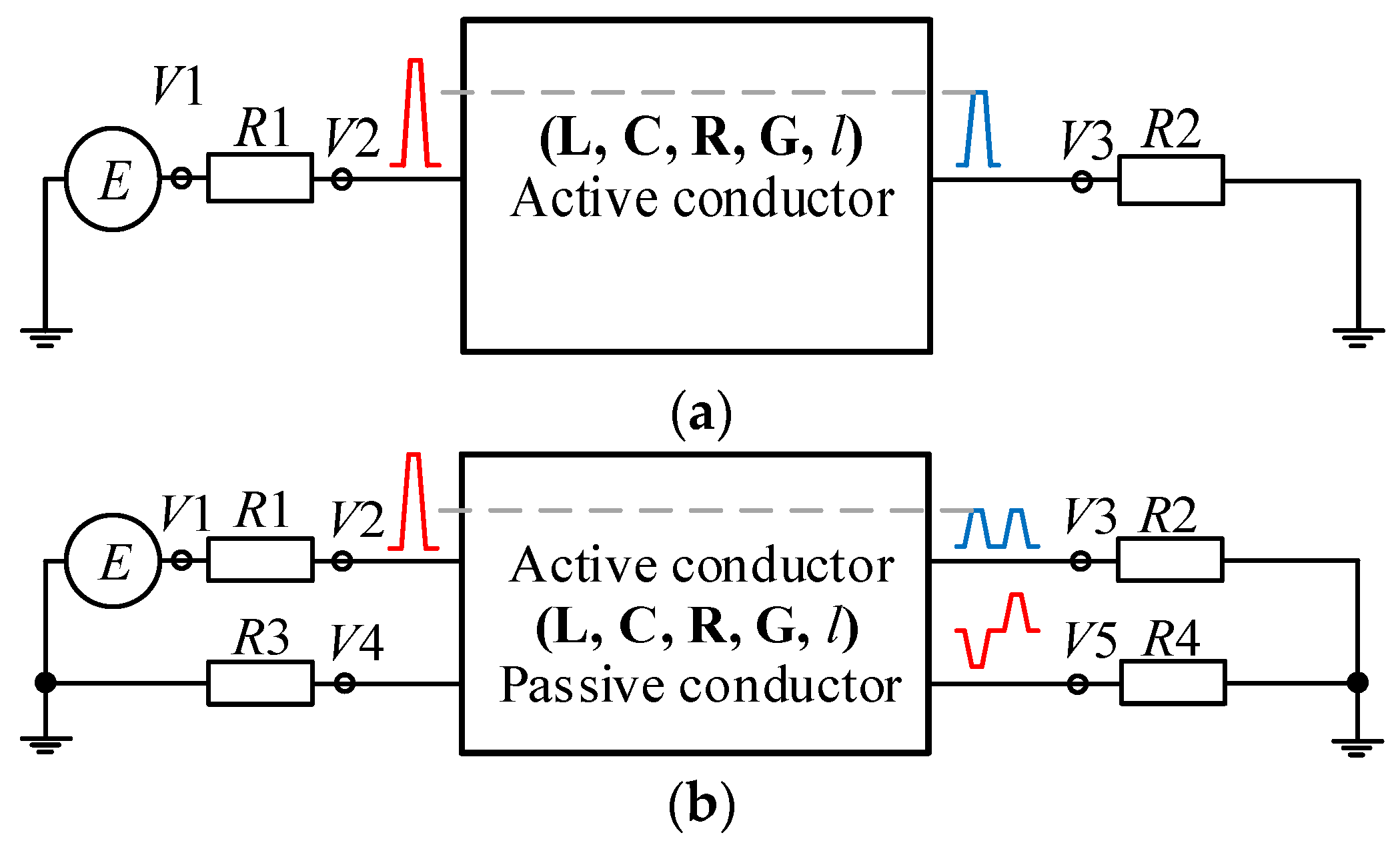
5[59]Obtaining the frequency dependences of the S-parameters of PCB prototypes with MR experimentally and comparing the results with those obtained using TALGAT softwareMR did not affect the useful signal and the compared results showed good agreement, with an average difference between them being up to 5 dB
6[60]Obtaining the frequency dependences of the S-parameters of PCB prototypes with MR after failure experimentally and comparing the results with those obtained using TALGAT softwareThe level of transmission ratio for the board with MR was lower than for the board without it even after failure, without affecting the useful signal, except some frequencies of the studied domain, due to the frequency shift
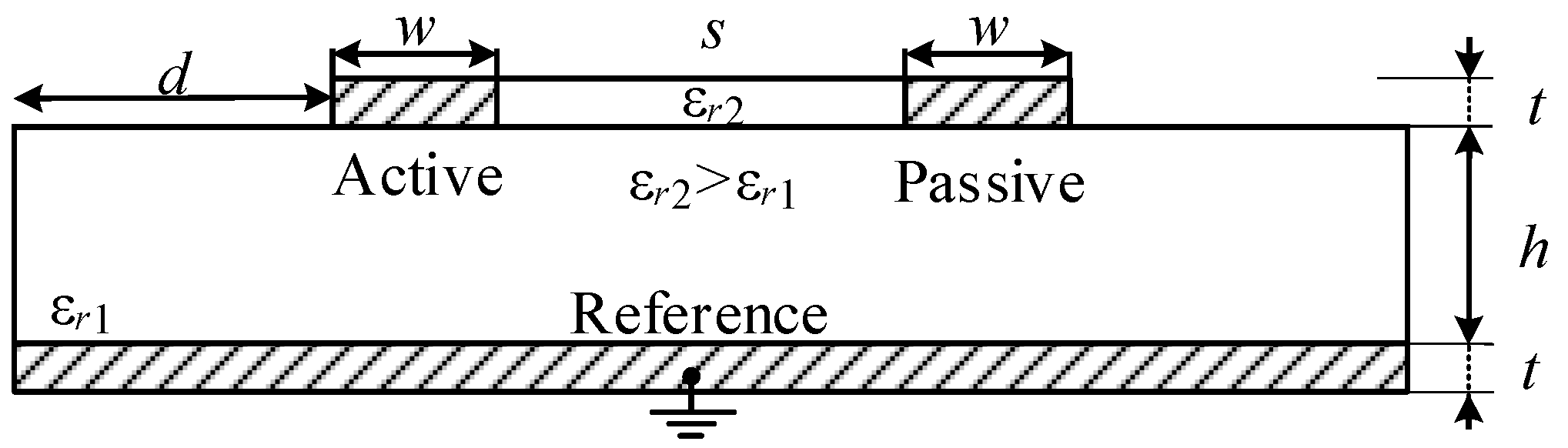
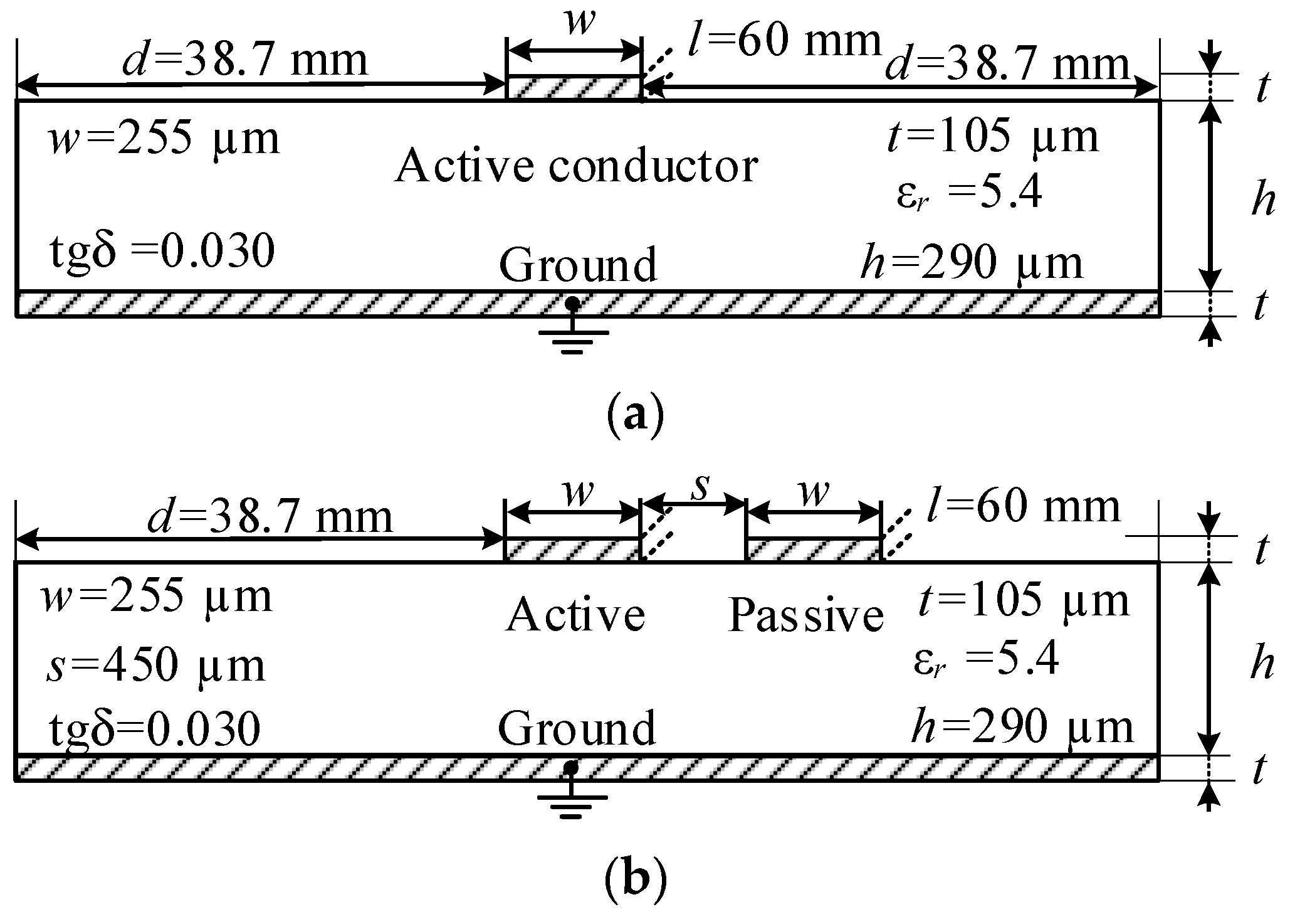
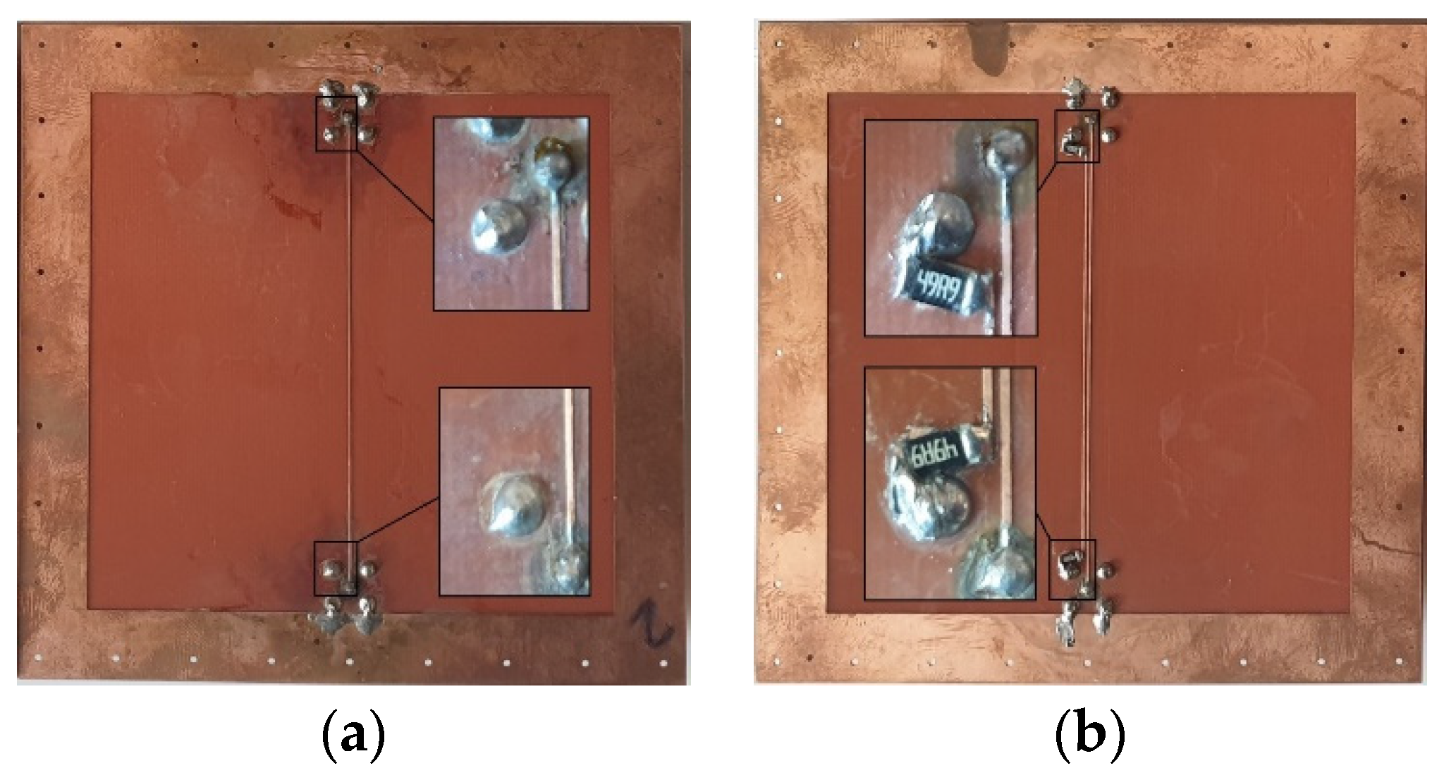
7[63]The RE levels from PCBs with MR were estimated before and after failure experimentally up to 2 GHz in a classical TEM-cellThe level of RE for the board with MR was lower than for the board without it even after failures, except at some frequencies of the studied domain, due to the frequency shift
8[64]The RE levels from PCBs with MR were estimated before and after failure experimentally up to 5 GHz in a Mini-TEM-cellThe possibility of using the MR layout and tracing approach was experimentally proven up to 5 GHz to both increase the reliability and ensure the electromagnetic compatibility, in terms of conducted emissions as well as radiated emissions
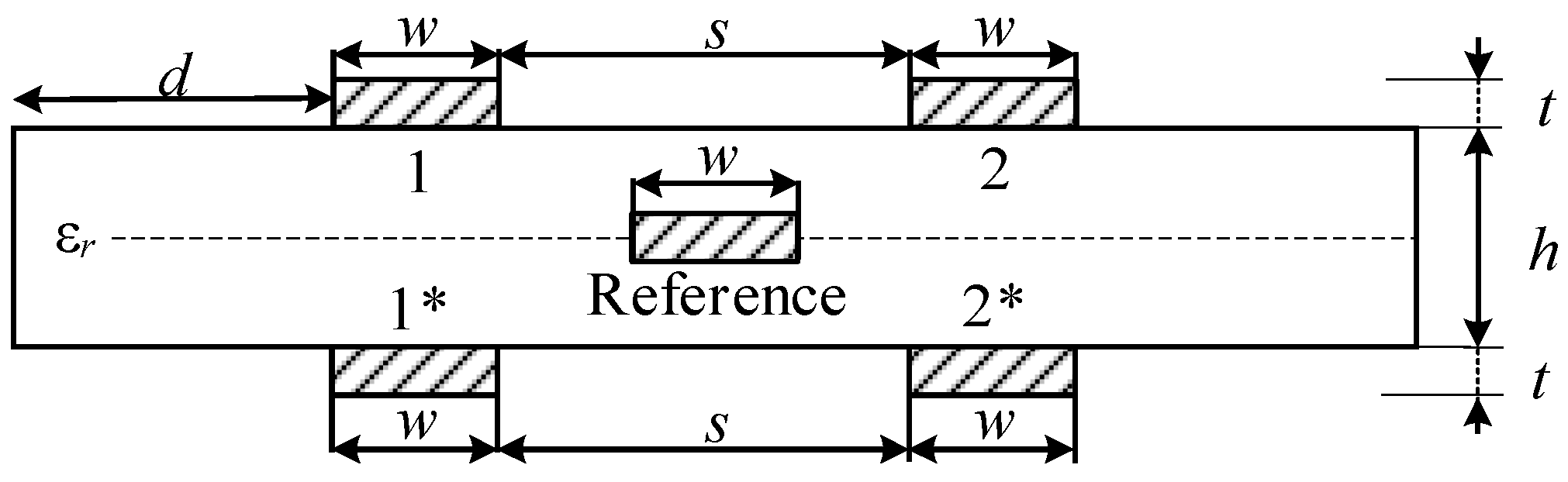
9[65]Obtaining the frequency dependences of the S-parameters of PCB prototypes with MR under climate impacts experimentallyThe level of the transmission ratio for the board with MR was lower than for the board without it. Meanwhile this reduction did not affect the useful signal. Moreover, all S-parameters of the prototypes decreased with increasing temperature and increased with decreasing temperature compared to the results obtained at room temperature over the entire frequency range, except for the resonance frequencies
10[66]Obtaining the frequency dependences of the S-parameters of PCB prototypes with MR after short circuit failure under climate impacts experimentallyRadioelectronic devices which used the MR layout and tracing approach worked under any climate condition even after short circuit failure, which improved their reliability and immunity against EMI
11[67]Obtaining the frequency dependences of the S-parameters of PCB prototypes with MR after open circuit failure under climate impacts experimentallyRadioelectronic devices which used the MR layout and tracing approach worked under any climate condition even after open circuit failure, which improved their reliability and immunity against EMI
Table 4. The Average differences in the calculated frequency dependences of the field intensities at the near and far ends of the central conductor of the TEM-cell in the climate chamber at −50 and 150 °C from the temperature of 23 °C for all PCBs.
PCBΔavg %Near end ΔNavg, %Far end ΔFavg, %
Without MR∑((U−50(f) − U23(f))/U23(f) %)/N−0.83.1
∑((U150(f) − U23(f))/U23(f) %)/N3.7−6.0
With MR∑((U−50(f) − U23(f))/U23(f) %)/N1.60.7
∑((U150(f) − U23(f))/U23(f) %)/N6.0−6.3
With MR-SC∑((U−50(f) − U23(f))/U23(f) %)/N2.05.2
∑((U150(f) − U23(f))/U23(f) %)/N7.8−6.6
With MR-OC∑((U–50(f) − U23(f))/U23(f) %)/N2.73.9
∑((U150(f) − U23(f))/U23(f) %)/N2.7−7.0
Table 5. The average differences in the calculated frequency dependences of the field intensities for the PCB with MR from those obtained for the other PCBs at the near and far ends of the central conductor of the TEM-cell in the climatic chamber at different temperatures.
PCB, Δavg %TemperatureNear end ΔNavg, %Far end ΔFavg, %
MR-Without MR
∑((UMR(f) − UNOMR(f))/UNOMR(f) %)/N
23−1.9−18.0
−50−0.9−17.2
150−2.6−18.4
With MR SC-With MR
∑((USCMR(f) − UMR(f))/UMR(f) %)/N
236.3−5.3
−507.6−4.4
1509.3−5.3
With MR OC-With MR
∑((UOCMR(f) − UMR(f))/UMR(f) %)/N
2317.38.8
−5018.98.5
15012.48.4
Publisher’s Note: MDPI stays neutral with regard to jurisdictional claims in published maps and institutional affiliations.

