Article

An Input-Series-Output-Parallel Cascaded Converter System Applied to DC Microgrids

1
Beijing Future Technology Innovation Centre for Electrochemical Energy Storage System Integration, North China University of Technology, Beijing 100144, China
2
School of Information Engineering, Beijing Institute of Petrochemical Technology, Beijing 102699, China
*
Author to whom correspondence should be addressed.
Symmetry 2023, 15(6), 1174; https://doi.org/10.3390/sym15061174
Submission received: 23 April 2023 / Revised: 21 May 2023 / Accepted: 26 May 2023 / Published: 30 May 2023

Abstract

:
Direct current transformer (DCT) is a key piece of equipment in direct current (DC) microgrids, and the mainstream topologies mainly include LLC resonant converter (LLC) and dual active bridge (DAB). In this paper, a novel bi-directional buck/boost + CLLLC cascade topology is proposed for the input-series-output-parallel cascade converter system of a DC microgrid. To solve the problem that frequency variation causes the converter to deviate from the optimal operating point, resulting in low efficiency, and the inability to achieve a soft switching function. The CLLLC converter operates near the resonant frequency point as a DCT, only providing electrical isolation and voltage matching, while the buck/boost converter controls the output voltage and the voltage and current sharing of each module. Compared to other cascaded converter systems, the cascaded converter proposed in this paper has high efficiency, simplifies the parameter design, and is suitable for wide input and wide output operating conditions. The system adopts a three-loop control strategy, establishes the small-signal modeling of the system, and its stability is verified by theoretical analysis and simulation. The simulation and experimental results verify the correctness of the proposed cascaded converter based on buck/boost + CLLLC and the effectiveness of the control strategy.

1. Introduction

In recent years, with the development of power electronics technology, the technical problems faced by DC transmission and distribution have gradually been solved. With better compatibility with distributed renewable energy sources, higher efficiency, and higher system reliability, DC microgrids have a broad development prospect. Distributed renewable energy (DER) is connected to the microgrid through power electronic converters (PEC) [1]. This paper presents a comprehensive literature review of DC-DC converter topologies used in DC microgrids [2,3]. Due to the existence of a buck-to-back process inside the converter, it is inevitable to add more switch tubes and energy storage components. Due to the pursuit of power density in converters, high-frequency converters usually need to solve switching losses and other issues. Therefore, high-frequency switches must achieve soft switching, and DC/DC converters with soft switching characteristics are gradually receiving attention [4,5]. Converters with bi-directional energy flow topologies are numerous while the topologies that guarantee high efficiency are limited. Several topologies will be described below.
The most widely used is the DAB converter, which has been widely studied by scholars due to its ability to achieve bi-directional power flow and soft switching technology, and its easy scalability. It has been applied in fields such as data centers, electric vehicles, and power electronic transformers. However, there are still some problems with current DAB converters, which usually only enable the soft switching of two switches at zero voltage over a narrow power range and are relatively complex to control [6,7,8,9].
The DC transformer with a DAB structure has the problem of current and voltage sharing, which requires additional circuit design to solve, increasing engineering costs and limiting its promotion in high-power range situations. However, traditional LLC resonant converters can only operate in a unidirectional power transmission state. Because of its asymmetric structure, there are differences in the resonant frequency and gain characteristics between the forward and reverse operation of the converter, which increases the complexity of converter parameter design and control [10,11].
The CLLLC resonant converter operates symmetrically in both forward and reverse directions, enabling bi-directional power transfer. Similar smooth switching characteristics to those of the CLLLC resonant converter can be achieved in bi-directional operation without the need for additional buffering auxiliary circuits [12,13].
Reference [14] introduces three DC/DC converter topologies suitable for high-power density and high-power applications. Ref. [15] introduces the average model of the ISOP DAB DC converter and analyzes the power distribution of its modular topology. Then, they propose an input-oriented fast dynamic response power-sharing control scheme to ensure the power-sharing ability and fast dynamic performance of DC converters. Ref. [16] proposes a wireless IVS control strategy for ISOP systems based on the positive output voltage gradient method, which can effectively improve the reliability and modularity of the ISOP system. Ref. [17] proposes a detailed design method for a bi-directional CLLLC resonant converter for an onboard charger (OBC), which can achieve a wide output voltage range. Ref. [18] presents a fully modular control strategy for input-series-output-parallel (ISOP) inverter systems. The proposed control strategy allows for a fully modular design without any interconnection of control signals between the constituent inverters, thus achieving superior modularity and reliability.
CLLLC best fits the resonant frequency point, and when the working frequency is not equal to the resonant frequency, there is an error between the theoretical analysis and the actual situation. In addition, when the operating frequency exceeds the resonant frequency, the converter cannot achieve the soft switching function, and the large range of frequency variations caused by large regulation is not conducive to the selection and efficiency of inductors, capacitors, and high-frequency transformers.
To solve these problems, this paper proposes a bi-directional buck/boost + CLLLC cascade structure [19,20]. By controlling the CLLLC converter to operate near the resonant frequency point, it exhibits the characteristics of a DC transformer, providing only electrical isolation and voltage matching, while the buck/boost converter controls the output voltage of each module. The system adopts a three-loop control strategy, and both the CLLLC converter and the buck/boost converter adopt dual closed-loop control. A voltage-sharing loop has been added to the buck/boost converter to achieve system input voltage sharing [21,22,23,24]. This design ensures the conversion efficiency of the resonant converter, as well as its good soft switching and dynamic characteristics. Compared to other topology structures mentioned, the advantages of a multi-converter combination system can be summarized: (1) reducing the power of submodules, facilitating device selection, and reducing costs. (2) The series-parallel structure of multiple converters facilitates system expansion and maintenance, while also improving system redundancy. Finally, the correctness and effectiveness of the parameter design and control method were verified through a 1 kw experimental prototype.

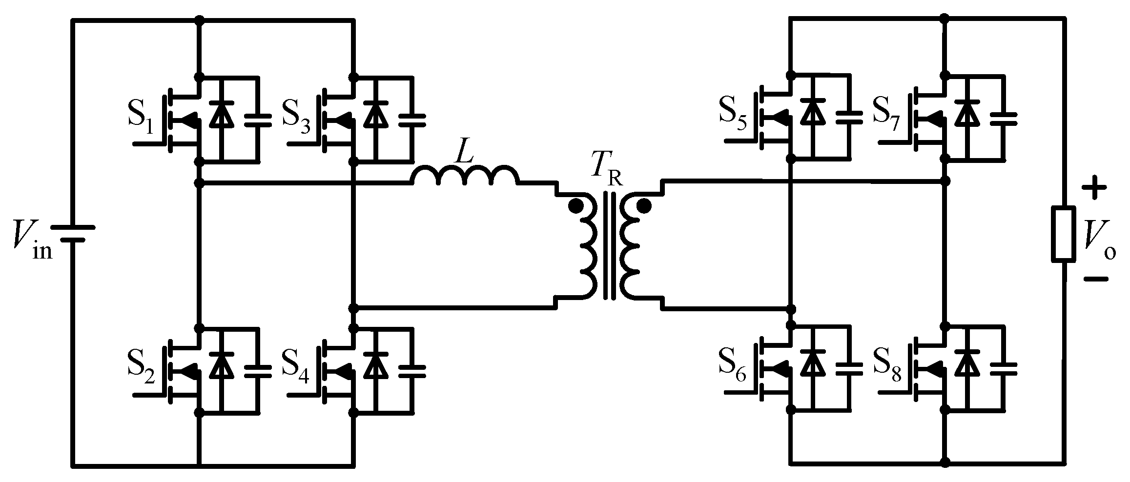
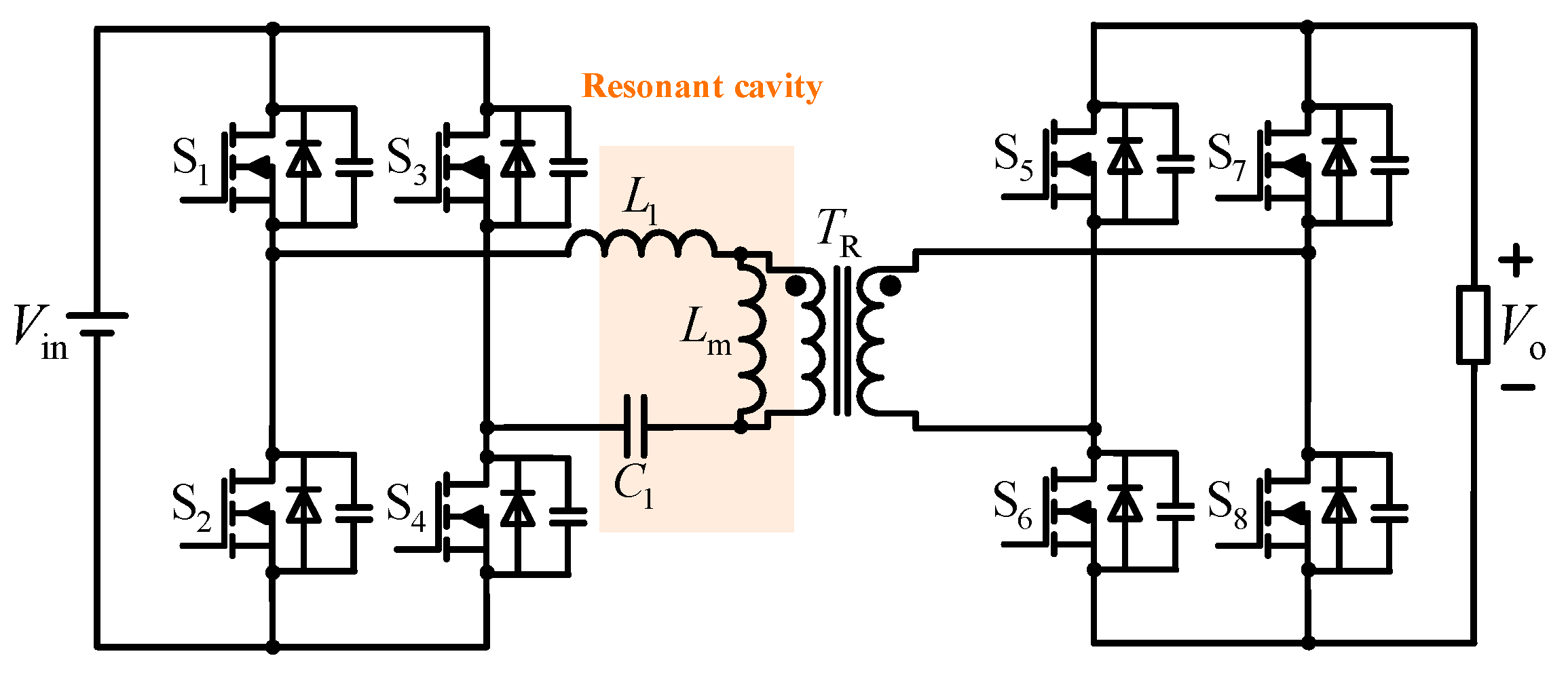
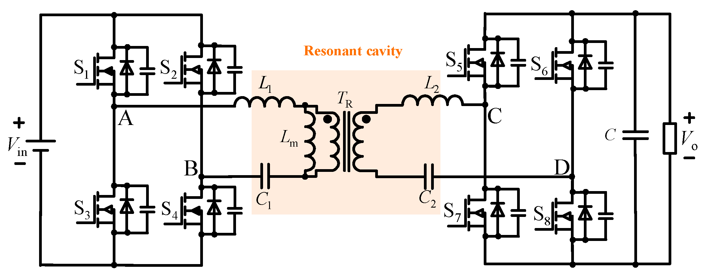
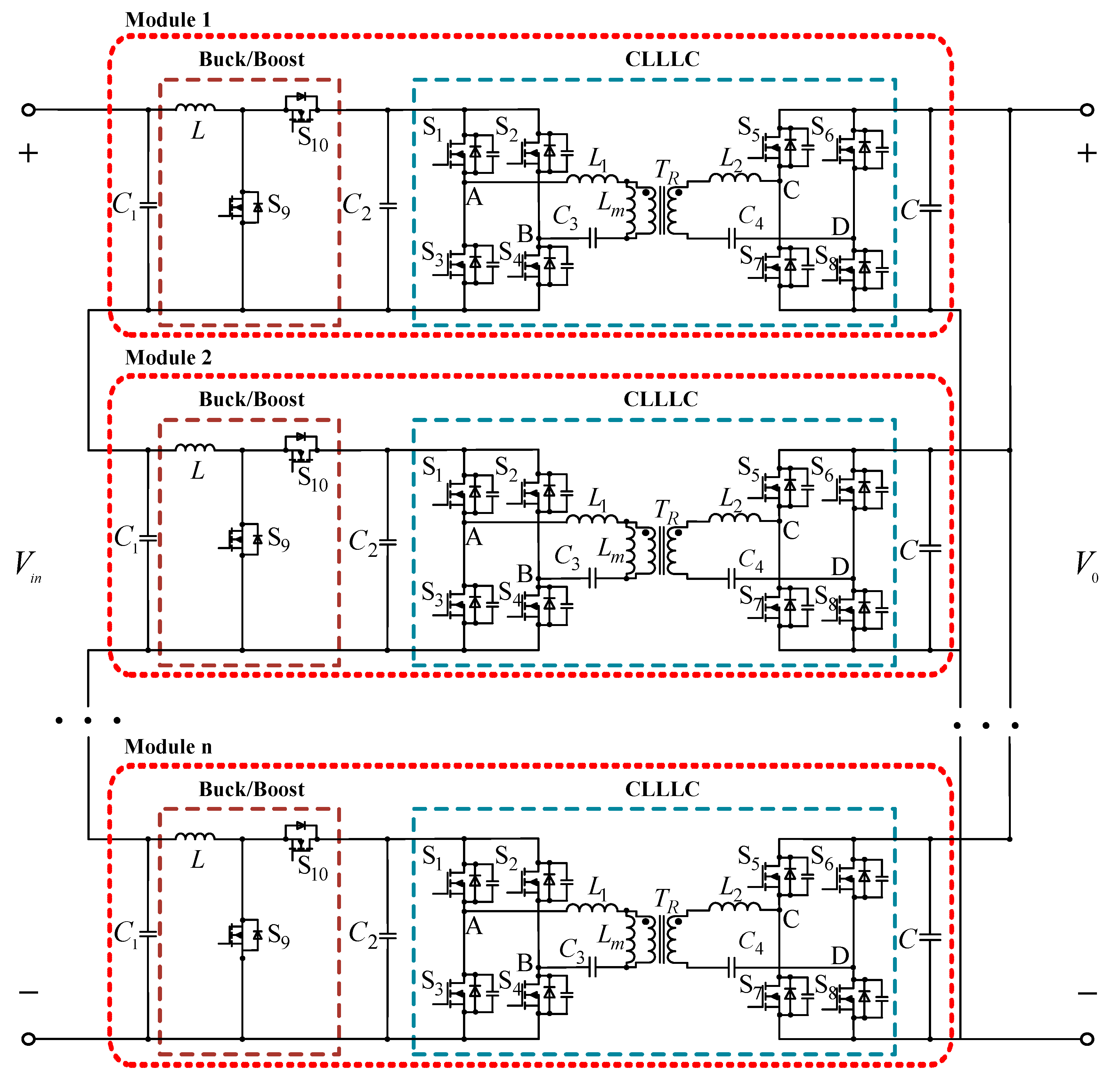
2. Converter Topology and System Structure

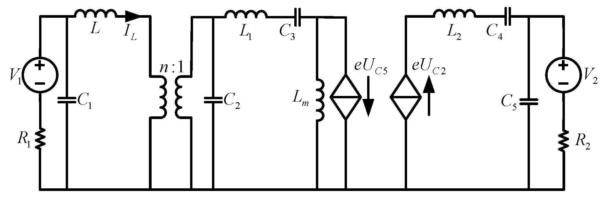
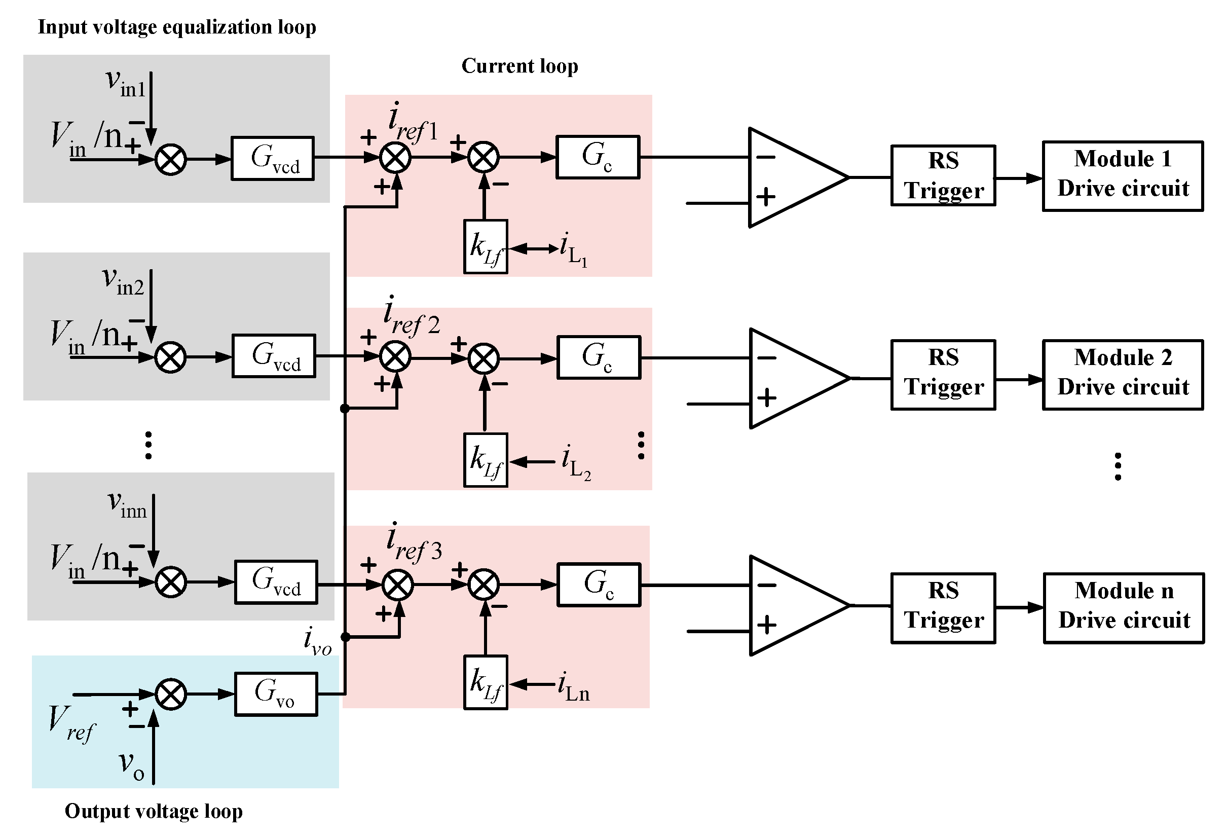
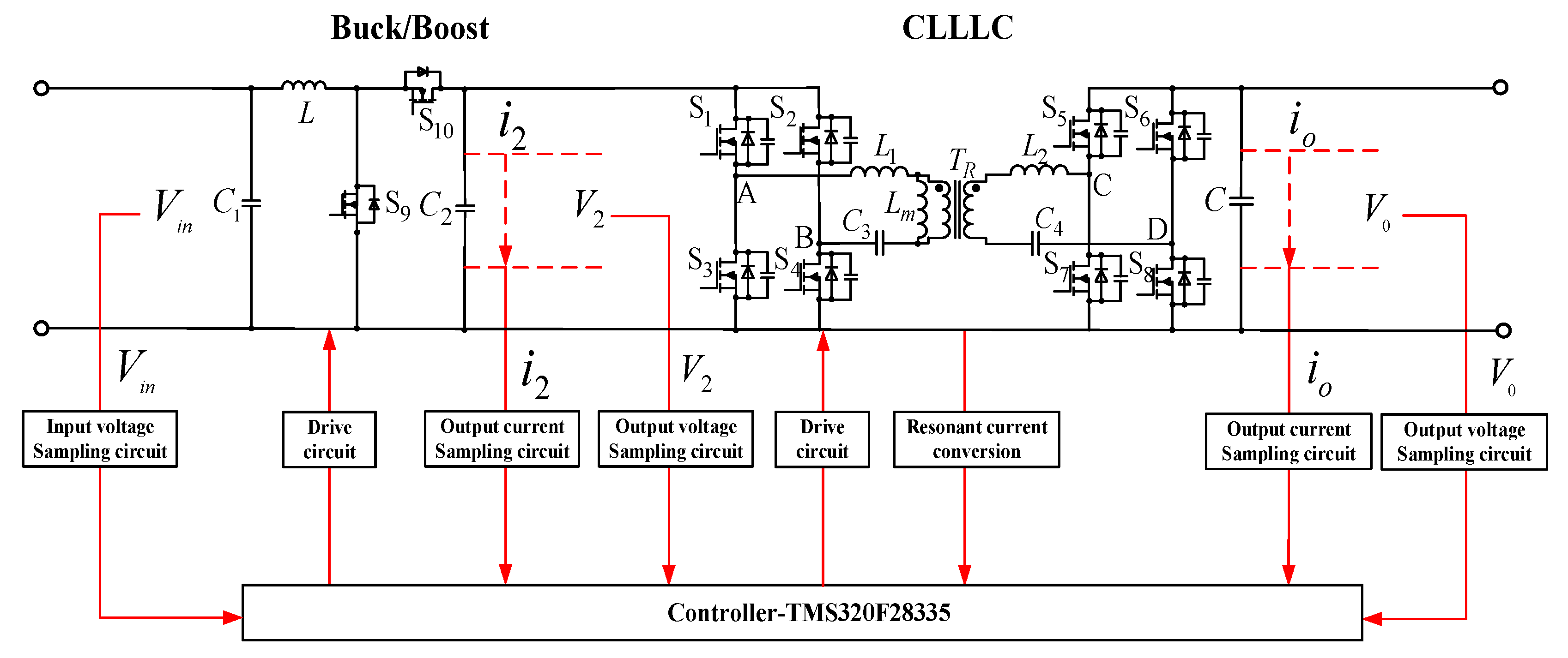
2.1. System Structure and Converter Topology

Figure 1 shows the topology of the DAB converter. Due to the presence of auxiliary inductor L, the DAB converter can achieve soft switching and zero voltage switching (ZVS) during operation, which also enables the efficiency of the DAB converter to reach over 97% in high-power applications [25,26].
In order to solve the problem of ZVS changing with load in DAB converters, LLC resonant converters have attracted widespread attention for their superior comprehensive performance. The LLC topology is shown in Figure 2. The LLC resonant converter has natural soft-switching characteristics and can achieve ZVS for the primary inverter switch tubes and ZCS for the secondary rectifier diodes over a wide range of input voltages and full loads, without an auxiliary network and with simple control.
In order to solve the problems of forward and reverse differences and the complex design of LLC converters, a CLLLC resonant converter topology is proposed, as shown in Figure 3.
Figure 4 shows the buck/boost converter topology. The buck-boost converter has the advantages of wide-range voltage conversion and bi-directional power transfer. It has received wide attention from scholars at home and abroad in recent years and is used in DC microgrids [27,28,29,30,31].
Figure 5 shows the DC transformer composed of a bi-directional buck/boost + CLLLC cascade converter; this new topology input side is connected in series and the output side in parallel, wherein the buck/boost converter works in voltage regulation mode [32] and the CLLLC converter works near the resonant frequency, through parameter design to achieve the role of DCX. A modular multi-converter series-parallel combination structure has been proposed, which is characterized by not only the normal operation of a single converter module but also the ability to achieve voltage/current sharing between multiple standardized modules through bus connection, achieving a modular combination structure of the system. Compared to other topologies, it has higher efficiency and fast dynamic response, which is suitable for high-power DC microgrids.

2.2. SubsectionAnalysis of Cascaded Converter Model

In this paper, we first establish the independent mathematical model of each module converter separately to obtain the equivalent circuit model. By cascading the circuit models of each level, we obtain the equivalent circuit model of the cascaded converter system so that we can establish the mathematical model of the cascaded converter system based on this circuit model. According to the buck/boost converter mathematical model and the CLLLC converter mathematical model, the steady-state equivalent circuit diagram of the buck/boost + CLLLC converter cascaded system can be obtained, as shown in Figure 6.
According to the above equivalent circuit diagram, the DC voltage gain M of the buck/boost + CLLLC cascaded converter is:
M = M B B M C L L L C
The state space averaging model of the buck/boost converter is obtained by averaging the modes over one switching cycle:
X ˙ s = A s X s + B s U s
where R is the buck/boost converter output impedance
A s = 1 C 1 R 1 0 1 C 1 0 1 C 2 R 1 D C 2 1 L 1 D L 0 , B s = 1 C 1 R 1 0 0 1 C 2 R 0 0
If X ˙ s = 0 , a static solution can be obtained according to Equation (3):
X s 0 = A s 1 B s U s
If the static working point X s 0 = V c 1 V c 2 I L T , therefore, the static operating point of the buck/boost converter is:
X s 0 = 1 D 2 R V 1 + 1 D R 1 V 1 D 2 R + R 1 1 D R V 1 + R 1 V 1 D 2 R + R 1 V 1 1 D V 1 D 2 R + R 1
where V is buck/boost converter output voltage.
Taking input variables U S = V , output variables V o = V 1 , the steady-state output voltage gain is:
M B B = V o U s = 1 D 2 R V 1 + 1 D R 1 V 1 D R V 1 + R 1 V
According to Figure 5, the input and output transfer functions of the CLLLC resonant converter are:
H ( j ω s ) = u CD u AB = Z m / / Z 2 + R eq Z 1 + Z m / / + R eq R eq R eq + Z 2
Z 1 = j ω s L 1 + 1 j ω s C 3 Z 2 = j ω s L 2 + 1 j ω s C 4 Z m = j ω s L m ω s = 2 π f
Defining k = L m / L 1 , h = L 2 / L 1 , g = C 4 / C 3 , ω 1 = 1 / L 1 C 3 , ω 2 = 1 / L 2 C 4 , ω n = ω s / ω 1 , and bring in simplification:
H j ω s = k ω s C 3 R eq ω s C 3 1 ω s L 1 + k ω s C 3 R eq + j k ω s 2 ω 1 2 + k h ω s 2 ω 1 2 + h ω s 2 ω 1 2 k k g h 1 g + 1 g ω 1 2 ω s 2
When the converter is operating at the resonant operating point, the imaginary part of the transfer function is zero, and the expression ωr of the resonant frequency containing the resonant network can be found in Equation (8):
k + h + k h ω r 4 k + h + k g + 1 g ω 1 2 ω r 2 + 1 g ω 1 4 = 0
Obtaining
ω r = b + b 2 4 a c 2 a ω 1
Among
a = k + h + k h b = k + h + k / g + 1 / g c = 1 / g
Defining the normalized frequency, the characteristic impedance of the resonant network, the system figure of merit, and in Equation (8), the reduced transfer function is:
H r ( j ω n ) = 1 j Q k k + h + k h ω n k + h + k g + 1 g 1 ω n + 1 g ω n 3 + 1 + 1 k 1 k ω n 2
The voltage gain of the CLLLC resonant converter is then obtained:
M C L L L C = 1 Q k 2 a ω n b ω n + c ω n 3 2 + 1 + 1 k 1 k ω n 2 2
When the tube is operating at resonance, Equation (11) is substituted into (13), and the converter gain in the quasi-resonant operating state is:
M C L L L C = 1 1 + 1 / g h k + k / g + h h
Substituting Equations (5) and (14) into Equation (1) to find the dc voltage gain M of the buck/boost + CLLLC cascaded converter is:
M = h 1 D 2 R V 1 + h 1 D R 1 V 1 D R V 1 + R 1 V 1 + 1 / g h k + k / g + h
According to the equivalent circuit diagram shown in Figure 5, the input-output transfer function G of the buck/boost + CLLLC cascaded converter is:
G = H j ω s G x u
At the static working point X s 0 , U s , D introduction of low-frequency small signals disturbances d ^ s , u ^ s . The small-signal model of the buck/boost converter is obtained by neglecting the small-signal disturbances of the second order and above.
x ^ ˙ s = 1 C 1 R 1 0 1 C 1 0 1 C 2 R 1 D C 2 1 L 1 D L 0 x ^ s + 1 C 1 R 1 0 0 1 C 2 R 0 0 u ^ s + 0 I L C 2 V c 2 L d ^ s
Among x ^ s = v ^ c 1 v ^ c 2 i ^ L T , u ^ s = v ^ 1 v ^ 2 T .
Status variables X s and input variables U s the transfer function is:
G x u = x ^ s s u ^ s s = s I A s 1 B s = R L C 2 s 2 + L s + 1 D 2 R P s R 1 1 D P s R 1 D P s R 1 L C 1 s 2 + L s + R 1 P s R C 2 s + 1 P s R 1 C 1 s + 1 D 1 P s
Among
P s = L C 1 C 2 R 1 R s 3 + L C 1 R 1 + C 2 R s 2 + L + C 2 + C 1 1 D 2 R 1 R s + R 1 + 1 D 2 R
Substituting Equations (6) and (18) into Equation (16) gives the input-output transfer function G of the buck/boost + CLLLC cascaded converter as:
G = R eq Z m / / Z 2 + R eq Z 1 + Z m / / + R eq R eq + Z 2 R L C 2 s 2 + L s + 1 D 2 R P s R 1 1 D P s R 1 D P s R 1 L C 1 s 2 + L s + R 1 P s R C 2 s + 1 P s R 1 C 1 s + 1 D 1 P s

3. Parametric Design

In order to make the ISOP system automatically achieve intermediate bus voltage equalization, the key is to ensure that the CLLLC converter presents DC transformer characteristics, and the converter parameters are designed based on this requirement. The resonant converter resonant network gain is approximately equal to 1, so the transformer transformation ratio is 1.5. The switch tube used in the CLLLC converter experiment is FGH40N60SFD, and its junction capacitance size is 2.3 nF. The maximum excitation inductance can be calculated to be 187 μH. In order to reduce the volume of the converter and reduce the influence of stray parameters on the resonant network, the transformer-integrated leakage inductance is used as the resonant inductance in the resonant network, and the leakage inductance affects the design of the transformer, so the k value is selected as 15, the excitation inductance Lm is 172 μH, and the resonant inductance L1 is 11.53 μH. Since the converter is designed to work at the resonance point, the resonant capacitance of 220 nF can be found according to the resonant inductance sought. According to the original secondary side, resonance parameters should be equivalent and equal, and the secondary side resonance parameters can be obtained. In summary, the parameter design of the system converter is shown in Table 1.
As the converter operates in buck mode, the output voltage is V1 on the low voltage side, so at this point let
v ^ 2 ( s ) = 0
The transfer function Gid(s) from the current loop d(s) to iL(s) can be obtained as:
G i d ( s ) = i ^ L ( s ) d ^ ( s ) v ^ 2 ( s ) = 0 = V 2 C s 1 + V 2 R L 1 C 1 s 2 + L s R + 1
The transfer function Gvi(s) from the voltage outer loop d(s) to iL(s) can also be obtained as:
G v i ( s ) = v ^ 2 ( s ) d ^ ( s ) v ^ 2 ( s ) = 0 = V 2 L 1 C 1 s 2 + L s R + 1
The transfer function Gvi(s) from the outer loop of the voltage to iL(s) to V1(s) is:
G v i ( s ) = v ^ 1 ( s ) d ^ ( s ) v ^ 2 ( s ) = 0 = 1 C 1 s + 1 R
Draw the Bode diagram of the loop voltage and current loop transfer function based on the parameters and Equations (23) and (24) of the buck/boost converter.
Define the PI controller expression as:
G PI ( s ) = k p + k i s
Figure 7 shows the Bode diagram of the controlled object of the voltage loop. The system gain in the low-frequency band is small and the slope is 0. The dynamic performance of the system is poor and there are steady-state errors, so a PI controller needs to be introduced to increase the gain of the system in the low-frequency band and increase the slope of descent. After system compensation, the system has a low-frequency slope of 20 dB/dec, a cutoff frequency of 100 Hz, and a phase margin of 120°, which is in line with the design criteria, and the PI controller parameters are reasonably designed.
As can be seen from the Bode diagram of the current loop-controlled object in Figure 8, the system gain in the low-frequency band is 40 dB, but the slope is 0. This makes the converter output have a steady-state error, and the PI controller needs to be introduced to increase the system slope down in the low-frequency band. After system compensation, the slope of the system in the low-frequency band is 20 dB/dec, the end frequency is about 1 kHz, the phase margin is 80°, which corresponds to the design standard, and the PI controller parameters are reasonably designed.

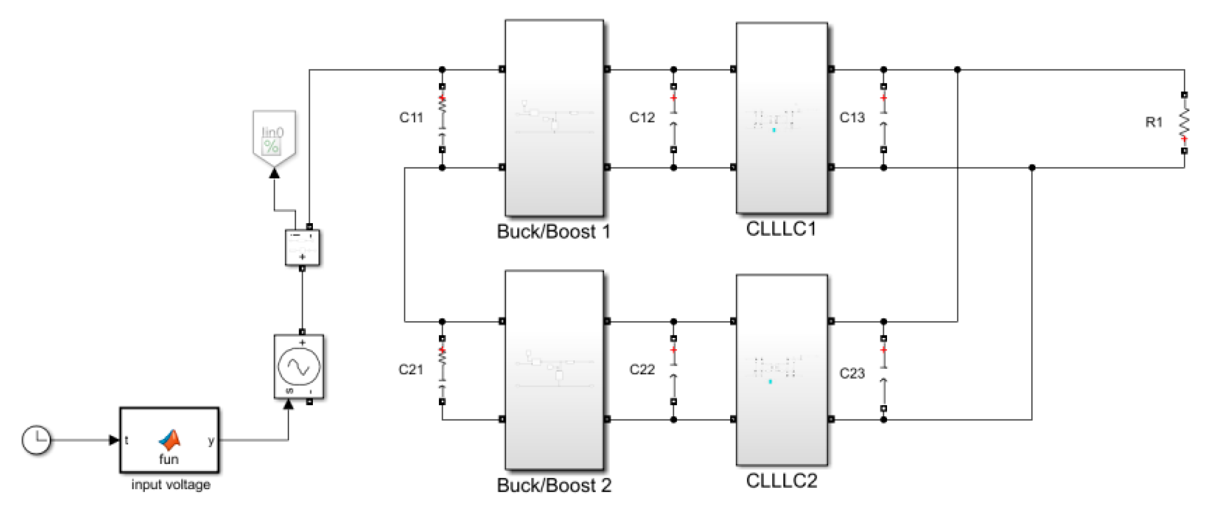
4. Simulation Results and Analysis

In order to verify the correct parameter design, dynamic performance, and stability of the proposed control strategy of the system, an ISOP system with two identical module parameters was built based on Matlab/Simulink to simulate load and input voltage sudden changes [33]. The simulation results verify that the system can naturally achieve voltage and current sharing of the intermediate bus under different load conditions. When the input voltage suddenly changes, the voltage of the intermediate busbar and the system output voltage change very little, and have a fast adjustment speed, achieving a good dynamic voltage-sharing effect.
The ISOP topology adopts a series structure on the input side and a parallel structure on the output side. The CLLLC converter in the submodule is equivalent to a wire. The buck/boost converter operates in buck mode, which controls the output voltage and equalizes the voltage and current of each module. The operation of the combined converter in buck mode is analyzed and Figure 9 shows a structural diagram of the three-loop control of an ISOP system. Figure 10 is the topology and control block diagram.
For the ISOP system, the key issue is to ensure that each module shares voltage on the input side and current on the output side. In recent years, many scholars have proposed various control schemes, which can be summarized into two categories: three-loop control and double-loop control. This system adopts three-loop control, which refers to the control system including the system output voltage loop, input voltage sharing loop of each module, and current inner loop of each module. Superposition of the output signal of the system output voltage loop and the output signal of the input voltage equalizing loop of each module as the given signal of the corresponding module current inner loop. The output of the current inner loop is compared with the sawtooth wave and processed accordingly to obtain the drive signal for each module’s switching tubes. Finally, the stability of the system output voltage and the input voltage equalization of each module is achieved. If the inner current loop of each module in the three-loop control strategy is removed and only the input voltage sharing loop and output voltage loop are retained, a dual loop control strategy can be obtained. All modules in the system share a voltage loop to ensure stable output voltage. The input voltage sharing ring directly adjusts the duty cycle of each module, increasing the duty cycle of modules with high input voltage. The duty cycle of modules with low input voltage is reduced, thereby achieving input voltage equalization.
Whether there is coupling between two control loops and whether the buck/boost converter operates in buck or boost mode, it will not affect the coupling relationship of the control loop. In order to ensure the stability of the system, an input voltage-sharing control strategy was adopted, which can be equivalent to the same input power for each module. Due to the consistent parameters of each module, the output current of each module is balanced and equal.

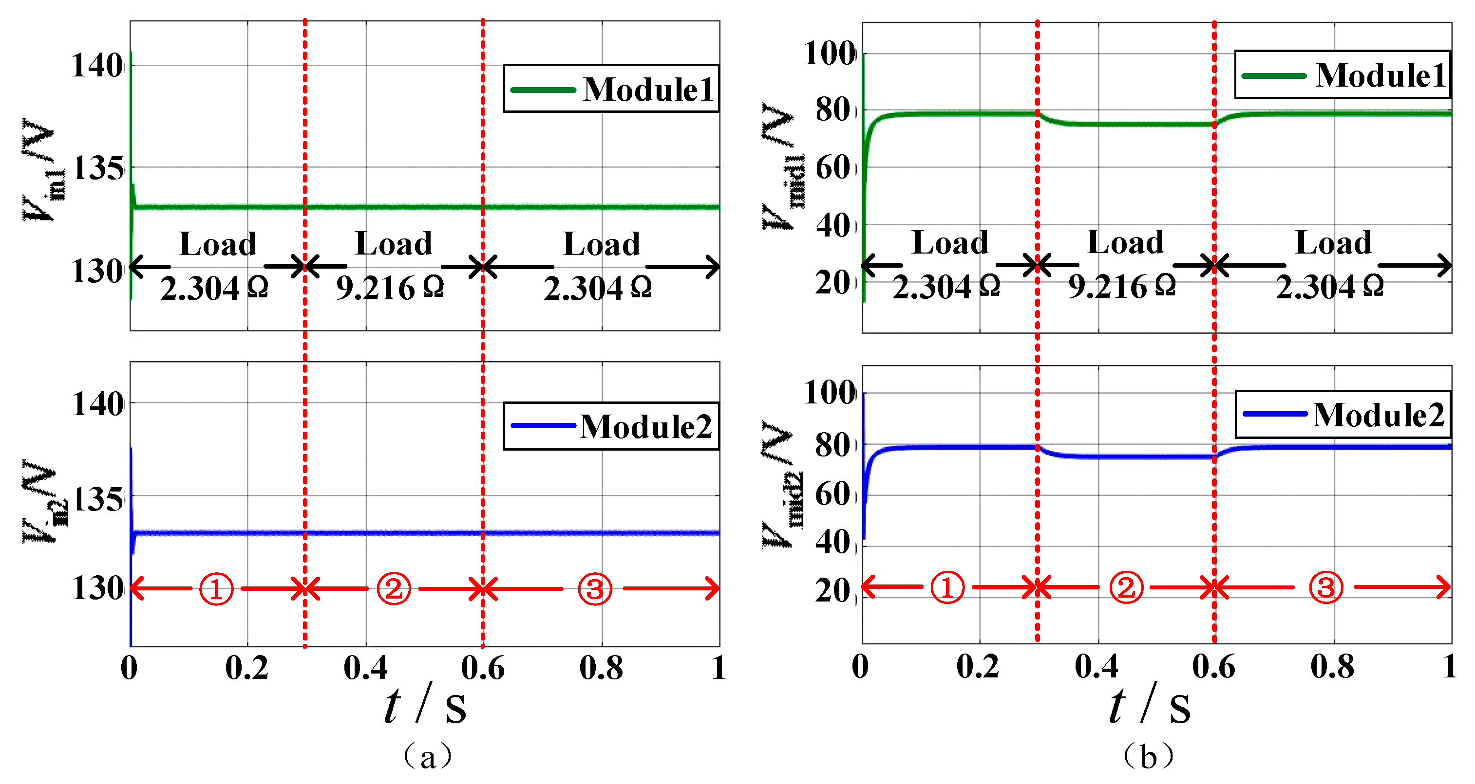
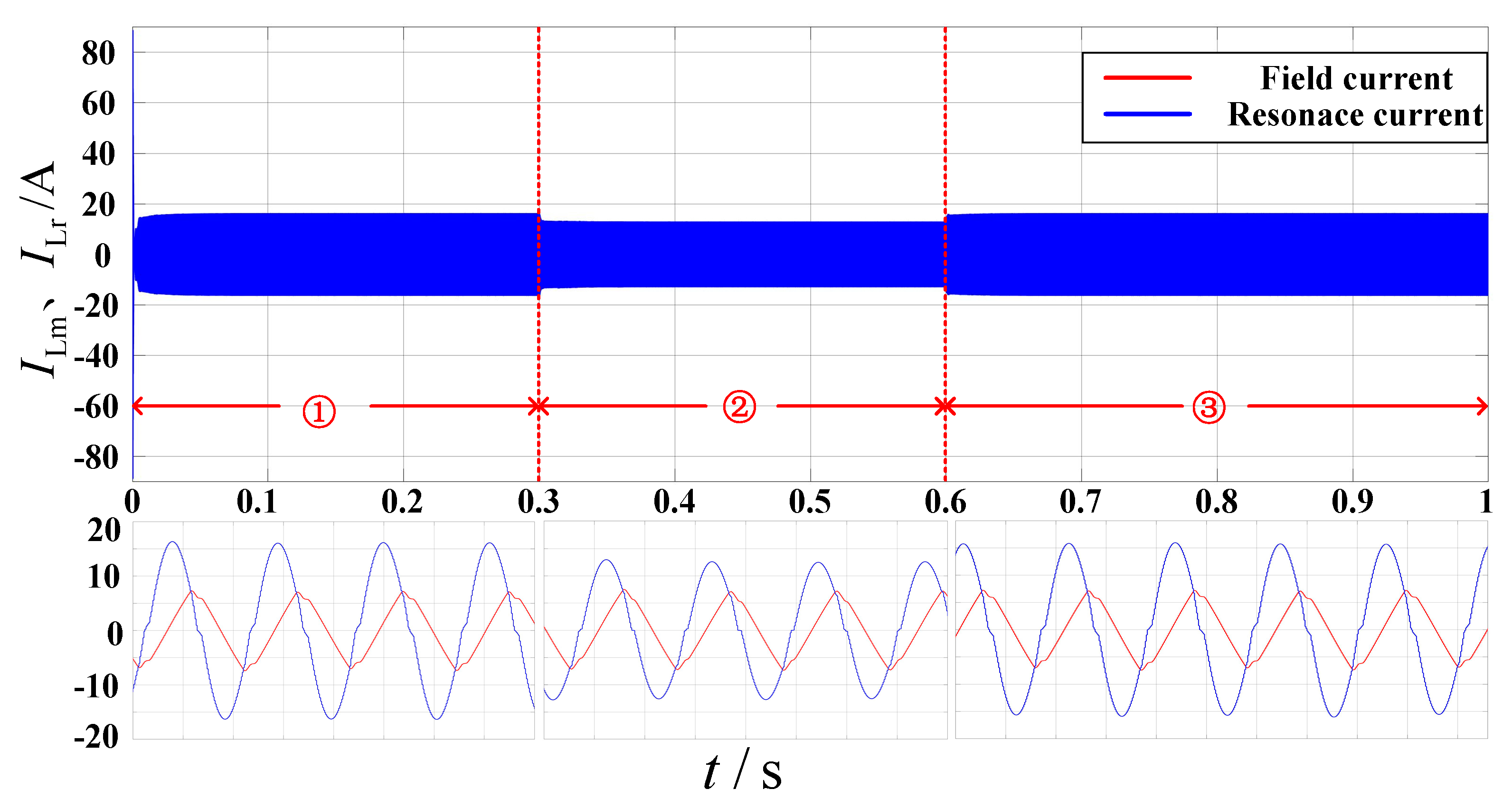
4.1. Simulation Experiment of Load Sudden Change

Figure 11 is the main circuit simulation model. Figure 12 is the control circuit simulation model.
Defined ① in Figure 13, Figure 14 and Figure 15 as a load of 2.304 Ω, ② load is 9.216 Ω, ③ load is 2.304 Ω. Figure 13a,b show the waveforms of the input voltage and intermediate voltage of each module when the system output load changes suddenly at full load and light load. The simulation results verify that each module can achieve equal input voltage distribution and a reasonable selection of control parameters.
The sudden load change is set to rise from 2.304 Ω to 9.216 Ω at 0.3 s and then fall to 2.304 ohms at 0.6 s. The output voltage and current waveforms of the system when the output load changes suddenly at full load and light load are shown in Figure 14. From the simulation results, it can be seen that when the system load power changes abruptly, the proposed control strategy can control the output voltage fluctuation of the converter to be less than 10%, and the adjustment time is within 100 ms.
Figure 15 shows the current waveform of the module resonant network. The simulation results show that changes in load can also cause changes in the current value of the resonant network. This is because the resonant current decreases under light load conditions, and the efficiency of the converter slightly decreases. However, under full load conditions, it can be seen that the CLLLC converter operates near the optimal operating point. Whether under light load or full load, the peak current of the excitation inductance remains basically unchanged, indicating that the conditions for achieving the ZVS of the switch under different loads are the same, which verifies the effectiveness of the resonant parameter design.

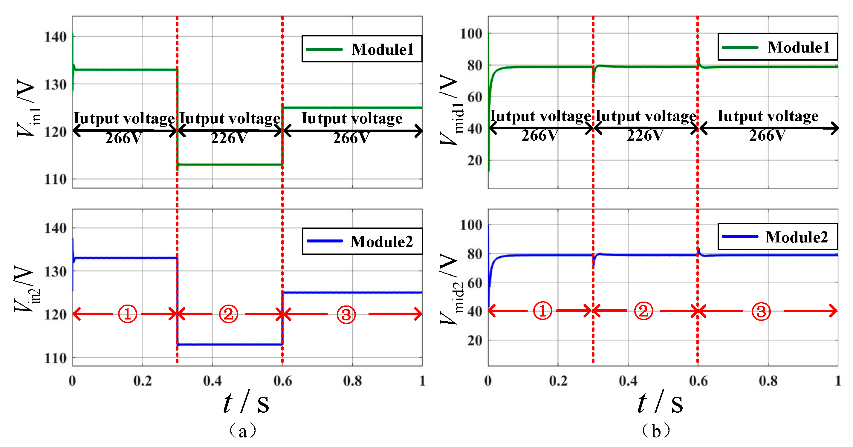
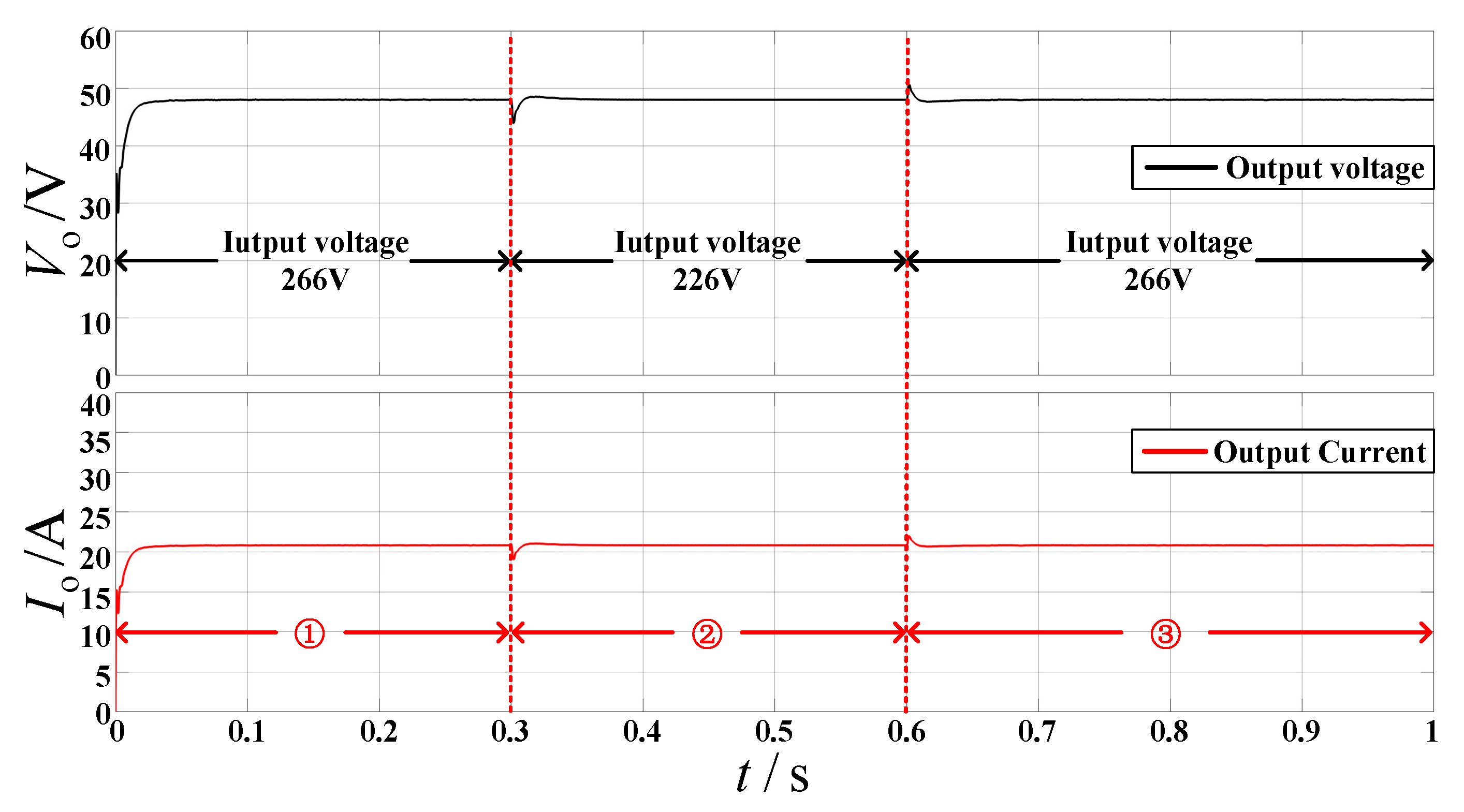
4.2. Simulation Experiment of Voltage Sudden Change

Defined ① in Figure 16, Figure 17 and Figure 18 as an input voltage of 266 V, ② input voltage of 226 V, ③ input voltage of 266 V. Figure 16 shows the waveform of the input voltage and intermediate stage voltage of each module in the system during a sudden voltage change. Due to the different values of input and output capacitance, the simulation results show that when the input voltage changes, the transient voltage distribution is not uniform due to the difference in capacitance between the input and intermediate stage voltages of each module.
Figure 17 shows the waveform of the system output voltage and current when the input voltage of the system undergoes a sudden change. The simulation results show that the proposed control strategy can control the output voltage fluctuation of the converter to be less than 2.4%, the adjustment time is within 40 ms, and the output voltage can be stable at 48V. The ISOP system not only has a fast-dynamic response speed but also achieves good dynamic voltage equalization.
Figure 18 shows the current waveform of the resonant network when the voltage suddenly changes. The simulation results show that the change in input voltage has no effect on the resonant current, and the converter is still in the optimal working state.
The ISOP system can only operate stably under input voltage-sharing control and adopts a three-loop control strategy. We designed the PI parameters of the buck/boost converter and determined the range of parameter values.

5. Experimental Results and Analysis

In order to verify the feasibility and effectiveness of the proposed automatic input voltage and output current sharing method, this chapter designed and completed a 1 kW ISOP system prototype consisting of two basic modules of buck/boost + CLLLC resonant converters.
The experimental results show that under the three-loop control strategy, it can respond quickly no matter when the load and voltage suddenly change. The CLLLC and buck/boost converter parameters are designed to use these submodules to form a buck ISOP system. We built an experimental platform based on the design parameters and conducted experimental analysis on the transient and steady-state characteristics of the ISOP system composed of submodules and multiple modules. The experimental platform and submodule physical platform are shown in Figure 19a,b.
The physical platform uses TMS320F28335 as the submodule control circuit, combined with a touch-screen display to form a system output display.

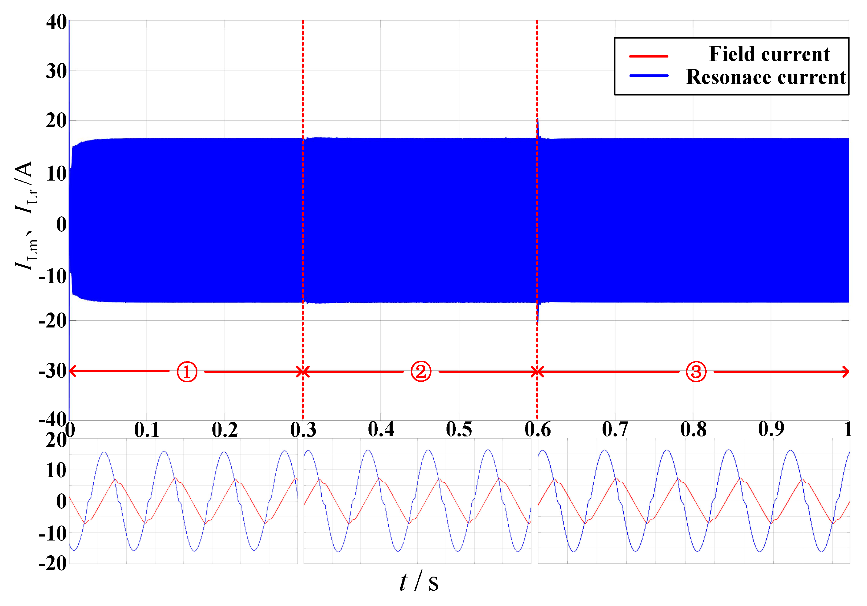
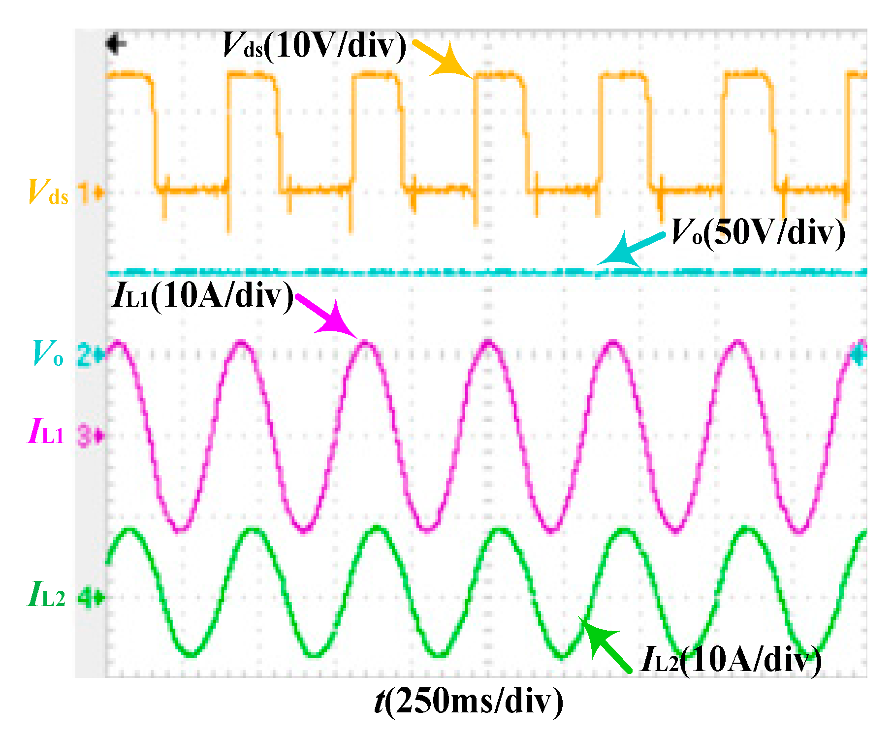
5.1. Steady-State Experiment of Sub-Moodle Voltage Reduction

The measured module drive signal, steady-state resonant current, and output voltage waveforms are shown in Figure 20 when operating in buck mode when the module input voltage is 134 V. The simulation results show that the output voltage of the CLLLC converter is 48 V and the resonant frequency is 100 kHz. The resonant current is in sinusoidal form, which means that the converter is located near the resonant operating point, where it is most efficient.

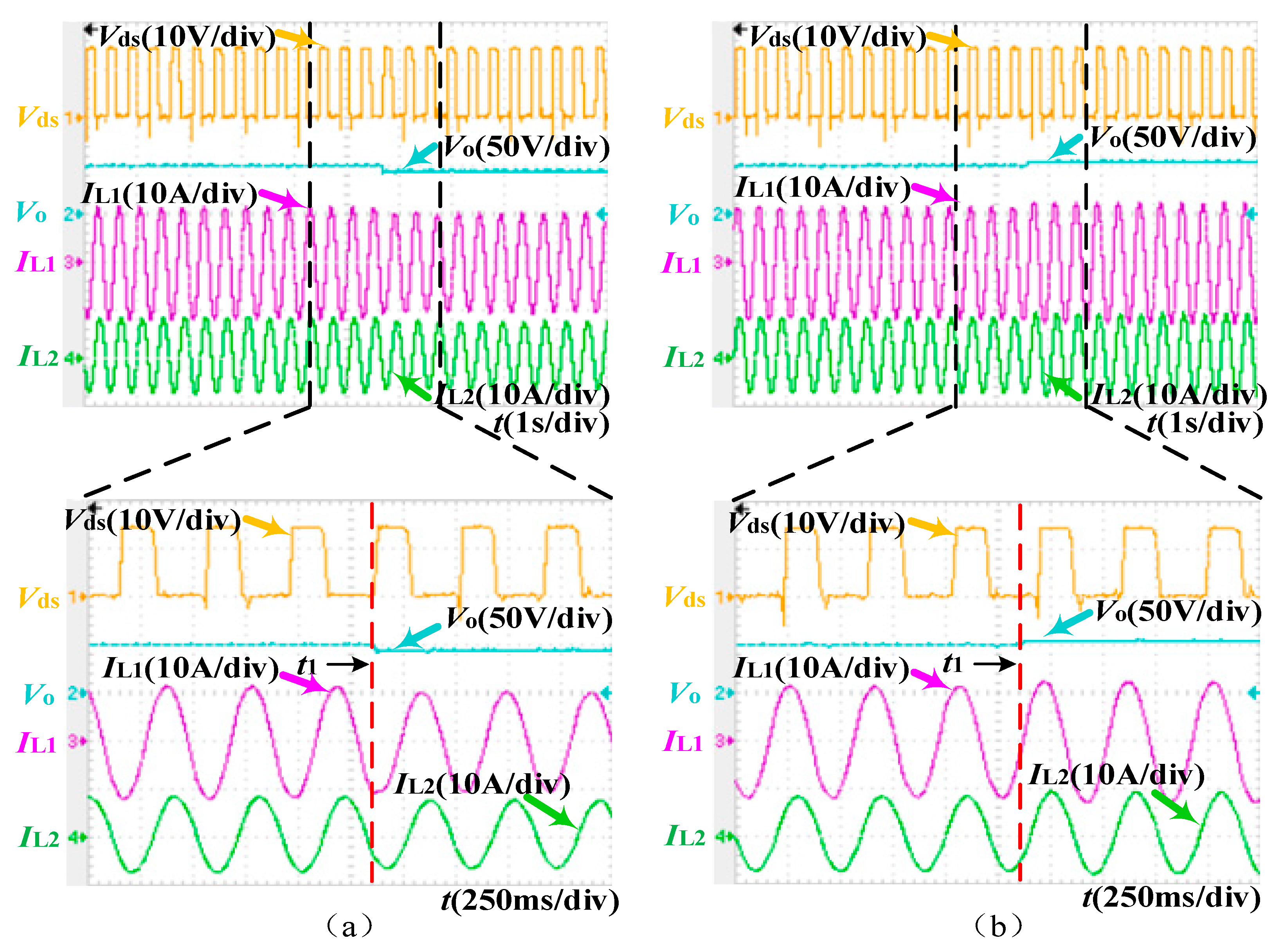
5.2. Dynamic Experiment of Sub-Moodle Voltage Reduction

Figure 21 shows the waveform of the driving signal, resonant current, and output voltage during output load switching. The load mutation of the submodule was set at t1, and the load suddenly changed from 4.608 Ω to 18.432 Ω. The resonant current changes from a sine wave to a delta wave, the current value decreases and the efficiency of the converter is reduced. At t2, the load suddenly changed from 18.432 Ω to 4.608 Ω, and the working point of the CLLLC converter returned to the resonance point.
When the input voltage suddenly changes from 134 V to 120 V at time t1, the waveform of the module output voltage and resonant current is shown in Figure 22a. The experimental results show that it cannot return to the rated input voltage of 48 V, and there is a deviation, but it is within 10%, meeting the indicator requirements. Similarly, when the input voltage suddenly changes to 145 V at t2, the output voltage also meets the indicator requirements, as shown in Figure 22b. There is no significant change in the amplitude of the resonant current in the resonant network under two operating conditions, and the CLLLC converter is always in the optimal working state.

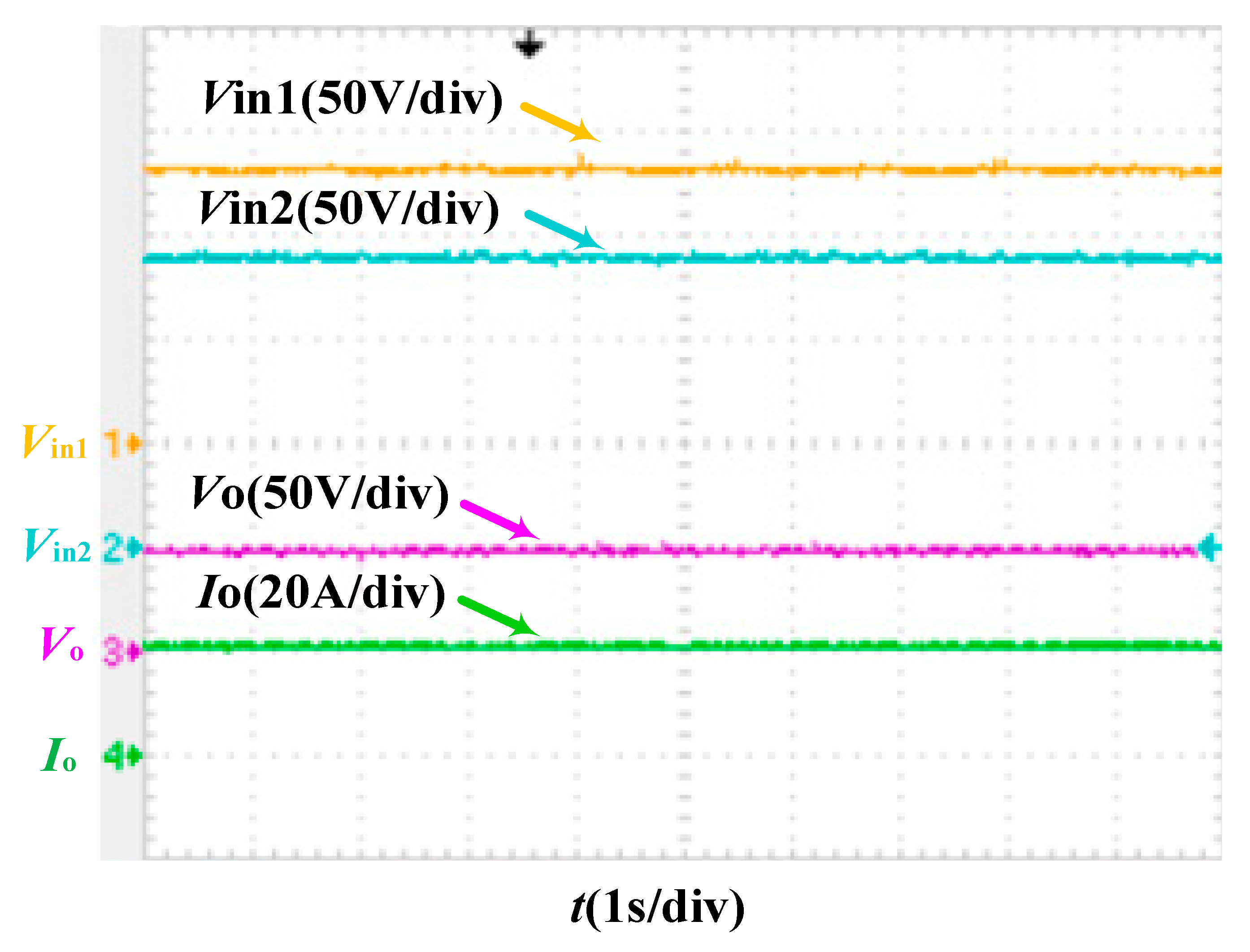
5.3. Steady State Experiment of ISOP System

The two modules are connected in series on the high-voltage input side and in parallel on the low-voltage output side to form an ISOP system. Figure 23 shows the ISOP system input and output voltage and current waveforms. At this time the system input voltage is 266 V, the two modules have approximately equal input voltage, module 1 input voltage is 130 V, module 2 input voltage is 135 V, the parallel output voltage is 48 V and the output current is approximately 19 A.

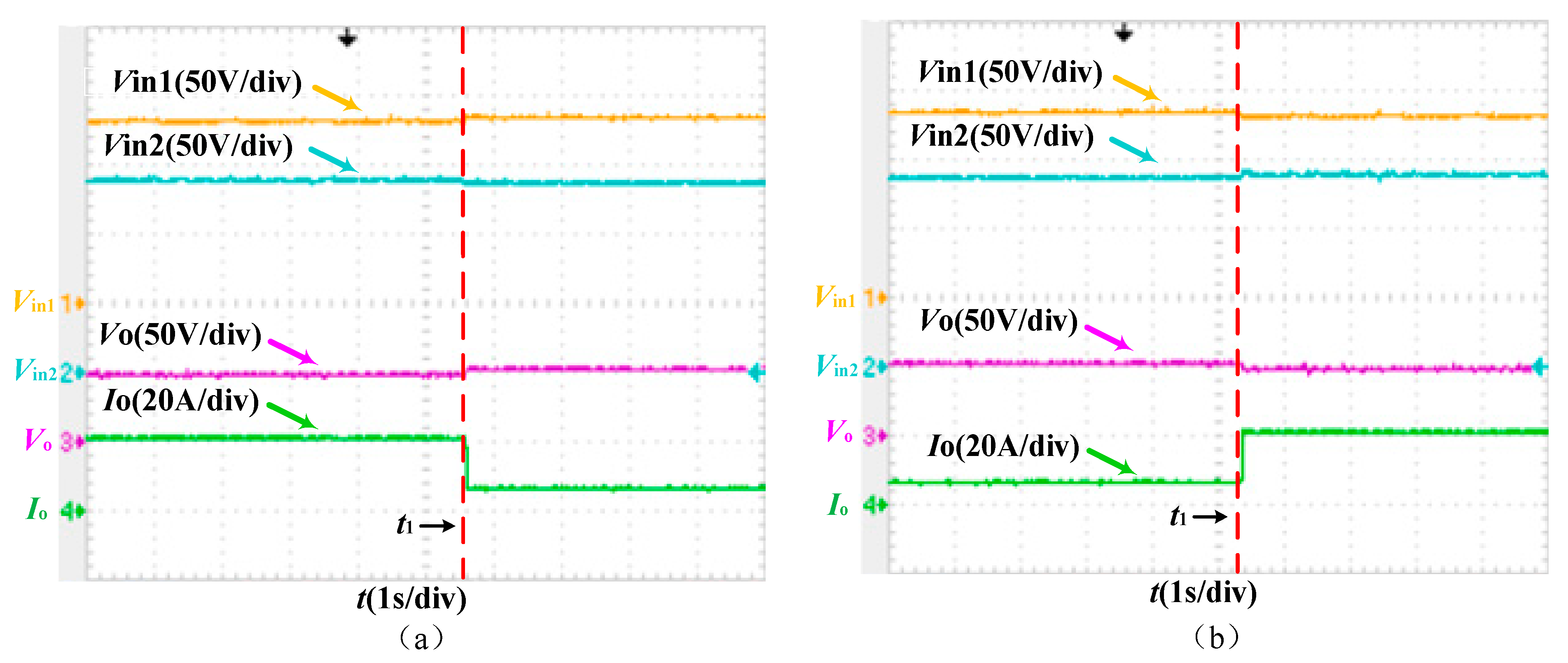
5.4. Dynamic Experiment of ISOP System

Figure 24a,b show the waveform of the input voltage and system output voltage and current of each module when the output load suddenly changes between 2.304 Ω and 9.216 Ω, respectively. The experimental results show that the input voltage of each module can be considered almost unchanged when the load suddenly changes, and the output voltage is stable at 48 V, which verifies the effectiveness of the control strategy.
Figure 25a,b show the waveform of the input voltage and system output voltage and current of each module when the input voltage suddenly changes between 266–226 V, respectively. From the experimental waveform, it can be seen that when the input voltage suddenly increases or decreases, the output voltage will slightly increase and decrease in a steady state. This is because the given reference value of the system output voltage changes, and under voltage mutation conditions, each module can evenly share the input voltage in a steady state.
The efficiency curve of the submodule and ISOP system is shown in Figure 26. When the output power is less than the rated power, the efficiency of the submodule and ISOP system tends to increase as the output power increases. However, when the output power reaches about 70–80% of the rated power, the efficiency is the highest, and it will decrease later, but overall, the efficiency is over 96%. In addition, the efficiency of the submodules is better than that of the ISOP system. The comparison of the theoretical and experimental results is shown in Table 2.

6. Conclusions

For a medium-power DC microgrid situation with high voltage input and low voltage output, we propose a new topology with a CLLLC+ buck/boost converter as a submodule of the ISOP system. This system adopts three-loop control, and the proposed control strategy can control the output voltage fluctuation of the converter to less than 10% when the system load power changes abruptly with a control time of less than 100 ms under the case of ±10% difference of input and output capacitance values. When the input voltage of the system changes abruptly, the proposed control strategy can control the output voltage fluctuation of the converter to less than 2.4%, the regulation time is within 40 ms, and the output voltage can be stabilized at 48 V. The proposed new topology has a quick dynamic response and an efficiency of more than 96%, which verifies the effectiveness of the adopted control strategy.

Author Contributions

Conceptualization, P.W. and M.L.; methodology, Y.W.; software, M.L.; validation, C.W. and Q.W.; formal analysis, Y.W.; investigation, J.L.; resources, J.L.; data curation, P.W.; writing—original draft preparation, M.L.; writing—review and editing, P.W.; visualization, P.J.; supervision, J.L.; project administration, P.W.; funding acquisition, P.J. and C.W. All authors have read and agreed to the published version of the manuscript.

Funding

This work was supported in part by the Beijing Natural Science Foundation under Grant 3232044, the National Natural Science Foundation of China under Grant 51907002, and the national key research and development plan 2018YFB1503005.

Data Availability Statement

Not applicable.

Acknowledgments

We are grateful for the equipment provided by the North China University of Technology.

Conflicts of Interest

The authors declare no conflict of interest.

References

  1. Mohammadhassani, A.; Teymouri, A.; Mehrizi-Sani, A.; Tehrani, K. Performance Evaluation of an Inverter-Based Microgrid Under Cyberattacks. In Proceedings of the System of Systems Engineering, Budapest, Hungary, 2–4 June 2020. [Google Scholar]
  2. Dahale, S.; Das, A.; Pindoriya, N.M.; Rajendran, S. An overview of DC-DC converter topologies and controls in DC microgrid. In Proceedings of the International Conference on Power Systems (ICPS), Pune, India, 21–23 December 2017. [Google Scholar]
  3. Babangida, M.; Md Pauzi, A.; Mufutau, A.S.; Mukhtar, F.H. DC-Based microgrid: Topologies, control schemes, and implementations. Alex. Eng. J. 2023, 70, 61–92. [Google Scholar]
  4. Oggier, G.G.; Ordonez, M. High-Efficiency DAB Converter Using Switching Sequences and Burst Mode. IEEE Trans. Power Electron. 2016, 31, 2069–2082. [Google Scholar] [CrossRef]
  5. Fakhri, N.; Naderi, M.S.; Farkoush, S.G.; Khoshdel, A.; Aghili, S.; Choi, S.K.; Rhee, S.B. Optimization of Impedance-Source Galvanically Isolated DC–DC Converters with Reduced Number of Switches. IEEE Access. 2022, 10, 3835–3847. [Google Scholar] [CrossRef]
  6. James, L.D.; Teixeira, C.A.; Wilkinson, R.H.; McGrath, B.P.; Holmes, D.G.; Riedel, J. Adaptive Modulation of Resonant DAB Converters for Wide Range ZVS Operation with Minimum Reactive Circulating Power. IEEE Trans. Ind. Appl. 2022, 58, 7396–7407. [Google Scholar] [CrossRef]
  7. Krismer, F.; Kolar, J.W. Closed Form Solution for Minimum Conduction Loss Modulation of DAB Converters. IEEE Trans. Power Electron. 2012, 27, 174–188. [Google Scholar] [CrossRef]
  8. Shuyu, C.; Sriram, V.B.; Tafti, H.D.; Kishore, K.R.; Li, Y.H.; Tripathi, A.; Pou, J. Modular DAB DC-DC converter low voltage side dc link capacitor two-stage charging-up control for solid state transformer application. In Proceedings of the 2017 Asian Conference on Energy, Power and Transportation Electrification (ACEPT), Singapore, 24–26 October 2017. [Google Scholar]
  9. Zeng, Y.; Pou, J.; Sun, C.; Mukherjee, S.; Xu, X.; Gupta, A.K.; Dong, J. Autonomous Input Voltage Sharing Control and Triple Phase Shift Modulation Method for ISOP-DAB Converter in DC Microgrid: A Multiagent Deep Reinforcement Learning-Based Method. IEEE Trans. Power Electron. 2023, 38, 2985–3000. [Google Scholar] [CrossRef]
  10. Wang, H.; Li, Z. A PWM LLC Type Resonant Converter Adapted to Wide Output Range in PEV Charging Applications. IEEE Trans. Power Electron. 2018, 33, 3791–3801. [Google Scholar] [CrossRef]
  11. Fang, X.; Hu, H.; Chen, F.; Somani, U.; Auadisian, E.; Shen, J.; Batarseh, I. Efficiency-Oriented Optimal Design of the LLC Resonant Converter Based on Peak Gain Placement. IEEE Trans. Power Electron. 2013, 28, 2285–2296. [Google Scholar] [CrossRef]
  12. Zong, S.; Fan, G.; Yang, X. Double Voltage Rectification Modulation for Bidirectional DC/DC Resonant Converters for Wide Voltage Range Operation. IEEE Trans. Power Electron. 2019, 34, 6510–6521. [Google Scholar] [CrossRef]
  13. Wang, X.; Liu, B.; Jiang, L.; Zhan, Z. Current Sharing Analysis for Novel Paralleled CLLLC Converters. IEEE Access. 2021, 9, 141307–141320. [Google Scholar] [CrossRef]
  14. De Doncker, R.W.A.A.; Divan, D.M.; Kheraluwala, M.H. A three-phase soft-switched high-power-density DC/DC converter for high-power applications. IEEE Trans. Ind. Appl. 1991, 27, 63–73. [Google Scholar] [CrossRef]
  15. Hou, N.; Gunawardena, P.; Wu, X.; Ding, L.; Zhang, Y.; Li, Y.W. An Input-Oriented Power Sharing Control Scheme with Fast-Dynamic Response for ISOP DAB DC–DC Converter. IEEE Trans. Power Electron. 2022, 37, 6501–6510. [Google Scholar] [CrossRef]
  16. Qu, L.; Wang, X.; Zhang, D.; Bai, Z.; Liu, Y. A High Efficiency and Low Shutdown Current Bidirectional DC-DC CLLLC Resonant Converter. In Proceedings of the 2019 22nd International Conference on Electrical Machines and Systems (ICEMS), Harbin, China, 11–14 August 2019. [Google Scholar]
  17. Chen, W.; Wang, G.; Ruan, X.; Jiang, W.; Gu, W. Wireless Input-Voltage-Sharing Control Strategy for Input-Series Output-Parallel (ISOP) System Based on Positive Output-Voltage Gradient Method. IEEE Trans. Ind. Electron. 2014, 61, 6022–6030. [Google Scholar] [CrossRef]
  18. Chen, W.; Jiang, X.; Cao, W.; Zhao, J.; Jiang, W.; Jiang, L. A Fully Modular Control Strategy for Input-Series Output-Parallel (ISOP) Inverter System Based on Positive Output-Voltage-Amplitude Gradient. IEEE Trans. Power Electron. 2018, 33, 2878–2887. [Google Scholar] [CrossRef]
  19. Yan, X.; Liu, C.; Liu, S.; Guo, X.; Zou, X. An Improved Interleaved Buck/Boost Integrated CLLLC Three-Port DC-DC Converter for Wide Input Range. In Proceedings of the 2021 IEEE 2nd China International Youth Conference on Electrical Engineering (CIYCEE), Chengdu, China, 15–17 December 2021. [Google Scholar]
  20. Rasoanarivo, I.; Tehrani, K.; Scalcon, F.P.; Nahid-Mobarakeh, B. A Dual Multilevel Adaptive Converter for Microgrid Applications. In Proceedings of the IECON 2022—48th Annual Conference of the IEEE Industrial Electronics Society, Brussels, Belgium, 17–20 October 2022. [Google Scholar]
  21. Madbouly, S.O.; Adel, M.S. A novel regulation inter-coupled control scheme for doubly fed wind induction system. Electromech. Energy 2016, 1, 8–16. [Google Scholar]
  22. Wang, Y.; Sun, Z.; Wu, Q.; Wang, Q.; Xiao, L. A Sensorless Input Voltage Sharing Control for ISOP DAB Converters. In Proceedings of the 2021 IEEE 1st International Power Electronics and Application Symposium (PEAS), Shanghai, China, 13–15 November 2021. [Google Scholar]
  23. Adel, M.S.; Mustafa, E.Ş. A flexible PV-powered battery-charging scheme for electric vehicles. IETE Tech. Rev. 2017, 34, 133–143. [Google Scholar]
  24. Mohamed, S.; Ebrahim, A.M.; Sharaf, A.M.; Atallah, A.S.; Emarah, A.S. Modified P&O technique for hybrid PV-battery smart grid integrated scheme. Electromech. Energy 2018, 3, 1–7. [Google Scholar]
  25. Sato, M.; Domoto, K.; Ishizuka, Y.; Manabe, S.; Okubo, H.; Yamaguchi, M.; Itagaki, A. High efficiency design for ISOP converter system with dual active bridge DC-DC converter. In Proceedings of the 2016 IEEE Applied Power Electronics Conference and Exposition (APEC), Long Beach, CA, USA, 20–24 March 2016; pp. 2465–2472. [Google Scholar]
  26. Kerachev, L.; Trinh, T.H.; Lembeye, Y.; Crebier, J.-C. Design and Implementation of a Highly Integrated Dual Active Bridge Microconverter. IEEE Trans. Power Electron. 2016, 31, 5635–5643. [Google Scholar] [CrossRef]
  27. Şahin, M.E.; Okumuş, H.İ. Comparison of different controllers and stability analysis for photovoltaic powered buck-boost DC-DC converter. Electr. Power Compon. Syst. 2018, 46, 149–161. [Google Scholar] [CrossRef]
  28. Aden, I.A.; Kahveci, H.; Şahin, M.E. Single input, multiple output DC-DC buck converter for electric vehicles. Electromech. Energy 2017, 2, 7–13. [Google Scholar]
  29. Ilyass, A.A.; Hakan, K.; Mustafa, E.Ş. Design and implementation of single-input multiple-output DC–DC buck converter for electric vehicles. J. Circuits Syst. Comput. 2021, 2, 2150228. [Google Scholar]
  30. Bote-Vazquez, Y.; Estevez-Encarnacion, E.S.; Ramirez-Hernandez, J.; Hernandez-Gonzalez, L.; Juarez-Sandoval, O.U. Predictive Current Control Design Methodology for DC-DC Basic Topologies: Buck, Boost and Buck-Boost Converters. In Proceedings of the 2021 IEEE International Autumn Meeting on Power, Electronics and Computing (ROPEC), Ixtapa, Mexico, 10–12 November 2021. [Google Scholar]
  31. Şahin, M.E.; Okumuş, H.İ. Parallel-Connected buck–boost converter with FLC for hybrid energy system. Electr. Power Compon. Syst. 2021, 48, 2117–2129. [Google Scholar] [CrossRef]
  32. Mustafa, E.Ş.; Frede, B. PV powered hybrid energy storage system control using bidirectional and boost converters. Electr. Power Compon. Syst. 2022, 49, 1260–1277. [Google Scholar]
  33. Mustafa, E.Ş.; Frede, B. A hybrid PV-battery/supercapacitor system and a basic active power control proposal in MATLAB/Simulink. Electronics 2020, 9, 129. [Google Scholar]
Figure 1. DAB converter topology.
Symmetry 15 01174 g001
Figure 2. LLC resonant converter topology.
Symmetry 15 01174 g002
Figure 3. CLLLC resonant converter topology.
Symmetry 15 01174 g003
Figure 4. Synchronous switching topology.
Symmetry 15 01174 g004
Figure 5. Schematic diagram of system structure and topology.
Symmetry 15 01174 g005
Figure 6. Steady-state equivalent circuit diagram of the buck/boost + CLLLC cascaded converter system.
Symmetry 15 01174 g006
Figure 7. Voltage loop-controlled object Bode diagram.
Symmetry 15 01174 g007
Figure 8. Current loop-controlled object bode diagram.
Symmetry 15 01174 g008
Figure 9. Three-loop control structure diagram of ISOP system.
Symmetry 15 01174 g009
Figure 10. Topology and control block diagram.
Symmetry 15 01174 g010
Figure 11. Main circuit simulation model.
Symmetry 15 01174 g011
Figure 12. Control circuit simulation model.
Symmetry 15 01174 g012
Figure 13. Input and intermediate stage voltage waveforms of each module during load changes suddenly. (a) Input voltage waveform; (b) intermediate stage voltage waveform.
Symmetry 15 01174 g013
Figure 14. Output voltage and current waveforms of ISOP system during load changes suddenly.
Symmetry 15 01174 g014
Figure 15. Current waveform of resonant network when load changes suddenly.
Symmetry 15 01174 g015
Figure 16. Input and intermediate voltage waveforms of each module with voltage changes suddenly. (a) Input voltage waveform; (b) intermediate stage voltage waveform.
Symmetry 15 01174 g016
Figure 17. Output voltage and current waveforms of ISOP system during sudden voltage changes.
Symmetry 15 01174 g017
Figure 18. Current waveform of resonant network when voltage changes suddenly.
Symmetry 15 01174 g018
Figure 19. Physical experiment platform and submodule physical platform. (a) Experimental platform; (b) submodule physical platform.
Symmetry 15 01174 g019
Figure 20. Resonant network current and output voltage waveforms of CLLLC converter in steady state.
Symmetry 15 01174 g020
Figure 21. Waveforms of output voltage and resonant current of submodules during sudden load changes. (a) The output load is increased to 18.432 Ω. (b) The output load is reduced to 4.608 Ω.
Symmetry 15 01174 g021
Figure 22. Waveforms of output voltage and resonant current of submodules during sudden voltage changes. (a) The input voltage changes to 120 V. (b) The input voltage changes to 145 V.
Symmetry 15 01174 g022
Figure 23. Waveform of ISOP system input–output voltage current in steady state.
Symmetry 15 01174 g023
Figure 24. Output voltage and harmonic current waveform of ISOP system during sudden load changes. (a) When the output load increases; (b) when the output load decreases.
Symmetry 15 01174 g024
Figure 25. Output voltage and harmonic current waveform of the ISOP system during sudden voltage changes. (a) The input voltage changes to 266 V. (b) The input voltage changes to 226 V.
Symmetry 15 01174 g025
Figure 26. Submodules and system efficiency curves.
Symmetry 15 01174 g026
Table 1. Buck/boost + CLLLC cascaded converter parameters.
Transformer NameParameter NameNumerical
Buck/boostHigh-side voltage V1134 V
Low-side voltage V272 V
Rated power P1500 W
Switching frequency fs120 kHz
Energy storage inductors L/mH0.6
Input capacitor C1/uF100
Output capacitor C2/uF120
Inductor current ripple Δ i L <20%
Output voltage ripple Δ V <5%
CLLLCHigh voltage V372 V
Low voltage V448 V
Rated power P2500 W
Switching frequency fs2100 kHz
Resonant inductance L1, L2/μH11.53, 5.12
Resonant capacitors C3, C4/nF220,560
Excitation inductance Lm/μH172
Table 2. Comparison of simulation and experimental data.
Work ConditionsOutputSystem SimulationSystem Experiment
Sudden load changeOutput voltage48 V47.7 V
Output current20.8 A20.4 A
Output power998.4 W973.08 W
Sudden voltage changeOutput voltage48 V47.5 V
Output current20.8 A20.5 A
Output power998.4 W973.75 W
Disclaimer/Publisher’s Note: The statements, opinions and data contained in all publications are solely those of the individual author(s) and contributor(s) and not of MDPI and/or the editor(s). MDPI and/or the editor(s) disclaim responsibility for any injury to people or property resulting from any ideas, methods, instructions or products referred to in the content.

