Abstract
In this paper, the effect of temperature on Single-Electron Transistor (SET) electrical behavior is investigated. In particular, a study of the current-voltage (I-V) curves according to parameter (temperature and gate voltage) variation is presented. Among others, the interesting phenomenon of the N-type negative differential resistance is reported as the temperature increases from absolute zero (0 K) to room temperature. Finally, theoretical analysis and simulation shows that the choice of the appropriate temperature and gate-voltage combination the SET I-V curves demonstrates either a negative differential resistance region, a switching effect, or a simple resistance behavior.
1. Introduction
The Single-Electron Transistor (SET) is considered to be one of the most promising devices in the field of nanoelectronics. This nanodevice may be considered as a sophisticated implementation of a field-effect transistor featuring a diminutive conducting island serving as the channel. This island is linked to both the drain and source terminals via tunnel junctions and is capacitive with respect to the gate. The gate plays a pivotal role in regulating the single-electron transfer process from the source to the drain. It is a fundamental device with ultra-low power consumption and high speed which can be used as random access memory. In addition, it also has the advantage of operating at room temperature [1]. The unique characteristic of SETs is the presence of an extremely small quantum dot in the channel. The fundamental physical principle of SETs is the tunneling effect through a Coulomb blockade [2,3,4]. The number of electrons inside the quantum dot is precisely controlled by the Coulomb blockade, thus, SETs show I-V characteristic curves that can exhibit Negative Differential Resistance (NDR) regions, which are expected to have new functionalities [5,6,7,8,9,10]. Theoretical investigation about the origin of NDRs has been reported in previous works [11,12,13].
This paper introduces simulations of typical Single-Electron Transistor (SET) I-V characteristics using MATLAB software. The primary focus of the study involves investigating the influence of gate voltage () values on - curves and examining the impact of temperature (T) on SET electrical behavior, utilizing classical models. Furthermore, the paper explores the combined effect of these two variables, gate voltage and temperature, on Negative Differential Resistance (NDR).
The motivation for this research stems from the discussions in the literature on negistor applications. Any device that demonstrates a NDR could be considered as a negistor device [14,15]. The applications of such devices as amplification, logic, memory, and chaotic oscillators are of high interest. These applications are predominantly based on resonant tunnel diodes and self-heating devices [16]. The paper aims to contribute to this specific direction by studying the NDR that arises from the SET. The NDR phenomenon is particularly relevant for optimizing negistor applications, offering potential improvements and novel functionalities. The simulations conducted using MATLAB provide a valuable tool for comprehending the intricacies of SET behavior under varying conditions. By systematically exploring the impact of gate voltage and temperature individually, as well as their combined effect, the study contributes to a deeper understanding of an SET’s electrical characteristics. The insights gained from this research may not only enhance the fundamental understanding of nanoelectronic devices, but also open up new possibilities for optimizing negistor-based applications. In summary, this work represents a valuable contribution to the field, employing simulations to analyze typical SET I-V characteristics and shedding light on the interplay between gate voltage, temperature, and the emergence of NDR in SETs. The findings may have implications for the design and optimization of negistor-based circuits with potential applications in various electronic systems.
2. Review of the Literature
2.1. Operational Principles
Single-Electron Transistors (SETs) seamlessly integrate quantum mechanical phenomena into the realm of nanoscale electronics, where the behavior of individual electrons takes center stage. Quantum dots serve as the foundational element for SETs, introducing discrete and quantized energy levels that move beyond classical boundaries [17].
The Coulomb blockade, a distinctive characteristic of SETs, highlights the devices’ responsiveness to changes in charge states. This phenomenon, rooted in quantum mechanics, manifests when the addition or removal of a single electron becomes energetically unfavorable, resulting in the suppression of electron transport. This intricate interplay between charge states and transport phenomena vividly illustrates the quantum essence inherent in SETs [18].
Quantum tunneling, a fundamental principle of quantum mechanics, plays a crucial role in the operation of Single-Electron Transistors (SETs). Functioning at the single-electron level, SETs utilize quantum tunneling to direct electrons through potential barriers, enabling their movement between quantum dots within the device. This quantum tunneling process serves as the pathway for the controlled flow of individual electrons, representing a departure from classical transport mechanisms [19].
The incorporation of a gate electrode into SETs introduces an additional layer of controllability into the quantum dynamics. By judiciously modulating the gate voltage, the number of electrons in the quantum dot can be finely tuned. This gate-controlled modulation not only showcases the versatility of SETs but also underscores the imperative role of external influences in navigating the intricate quantum landscape [20].
Charging energy, dependent on the capacitance of the quantum dot, emerges as a pivotal factor shaping the behavior of SETs. This energy parameter, representing the energy required to alter the charge state of the quantum dot, plays a decisive role in influencing the overall dynamics of the SET. The delicate balance between quantum coherence and external control is encapsulated in this charging energy, shaping the quantum landscape of these devices [21].
Operating at the single-electron level, SETs epitomize precision in electronic control. Manipulating the charge state of the quantum dot results in quantized changes in conductance, affording precise control over electron flow [22]. The inherent quantum coherence of these devices, allowing them to exist in multiple states simultaneously, contributes to their unique and versatile behavior [23].
In summary, Single-Electron Transistors represent a captivating integration of quantum mechanics and nanoelectronics. Their operational principles, fueled by quantum dots, the Coulomb blockade, tunneling, and controlled modulation, position them as promising candidates for emerging technologies where the manipulation of individual electrons is not just advantageous but imperative.
2.2. Temperature Effects in Nanoelectronic Devices
The literature on temperature effects in nanoelectronic devices encompasses a broad spectrum of research aimed at understanding and optimizing device performance under varying thermal conditions. A foundational aspect involves exploring the impact of temperature on electron transport properties in nanoscale devices, examining charge carrier mobility, conductivity, and overall device functionality at different temperature regimes [24]. As devices continue to shrink in size, thermal management becomes a critical concern. Researchers delve into methods for efficient heat dissipation and addressing temperature-induced reliability issues, particularly as devices operate in environments with fluctuating thermal conditions [25].
In the realm of nanoscale devices, quantum effects come to the forefront, and their interplay with temperature fluctuations becomes a subject of investigation. This includes studies on quantum dots and single-electron transistors with the aim of comprehending and controlling quantum phenomena under different temperature conditions. Reliability is a key consideration, and the literature explores how temperature variations impact the lifespan and degradation mechanisms of nanoelectronic devices. Understanding these factors is crucial for designing robust devices capable of withstanding extreme temperature environments [26].
Thermoelectric materials and devices are garnering attention for their potential in energy harvesting and efficient cooling. Researchers investigate the temperature-dependent behavior of thermoelectric nanomaterials and their application in nanoelectronics to harness temperature differentials for practical purposes [27].
As emerging technologies like neuromorphic computing and quantum computing gain traction, studies focus on how temperature influences their performance. This involves examining the thermal characteristics of these innovative devices and understanding how temperature fluctuations affect their functionality.
3. Results—Analysis Simulation
The behavior of Single-Electron Transistors (SETs) has been comprehensively explored through theoretical analysis and simulation, with a focus on various parameters. To simplify our understanding, we envision our nanodevice as comprising a semiconducting channel separated by an insulator layer, surrounded by a metallic gate. The application of a positive gate voltage is observed to lower the energy levels in the channel, rendering it an n-type channel. Conversely, a negative gate voltage operation reduces the number of electrons, resulting in a p-type channel. The key mathematical equations governing the current–voltage SET curves in this study are extensively detailed in [28].
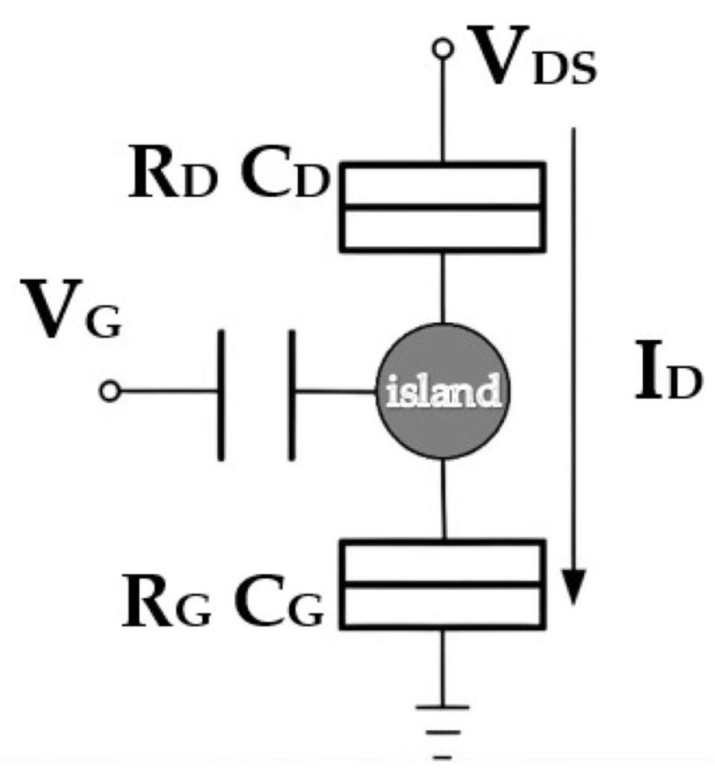
In Figure 1, the schematic representation of an SET is depicted, where the top and bottom terminals are designated as the source and the drain terminals, respectively. Various parameters play crucial roles in shaping the device’s characteristics, including (gate capacitance), and (junction resistances), as well as and (junction capacitances) [11].

Figure 1.
Typical schematic representation of a SET, including, terminal annotation and the parameters influencing its behavior.
The intricate interplay of these parameters contributes to the overall behavior of an SET. Positive and negative gate voltage operations induce distinct changes in the channel, influencing its conductivity and electron population. The equations described in [28] serve as fundamental tools for understanding and predicting the current–voltage characteristics of SETs under different conditions.
This theoretical framework, coupled with the simulated results, provides a valuable foundation for exploring the potential applications and optimizations of SETs in nanoelectronics. The ability to control electron transport through the manipulation of gate voltages and other device parameters opens up avenues for advancements in electronic circuits and systems at the nanoscale.
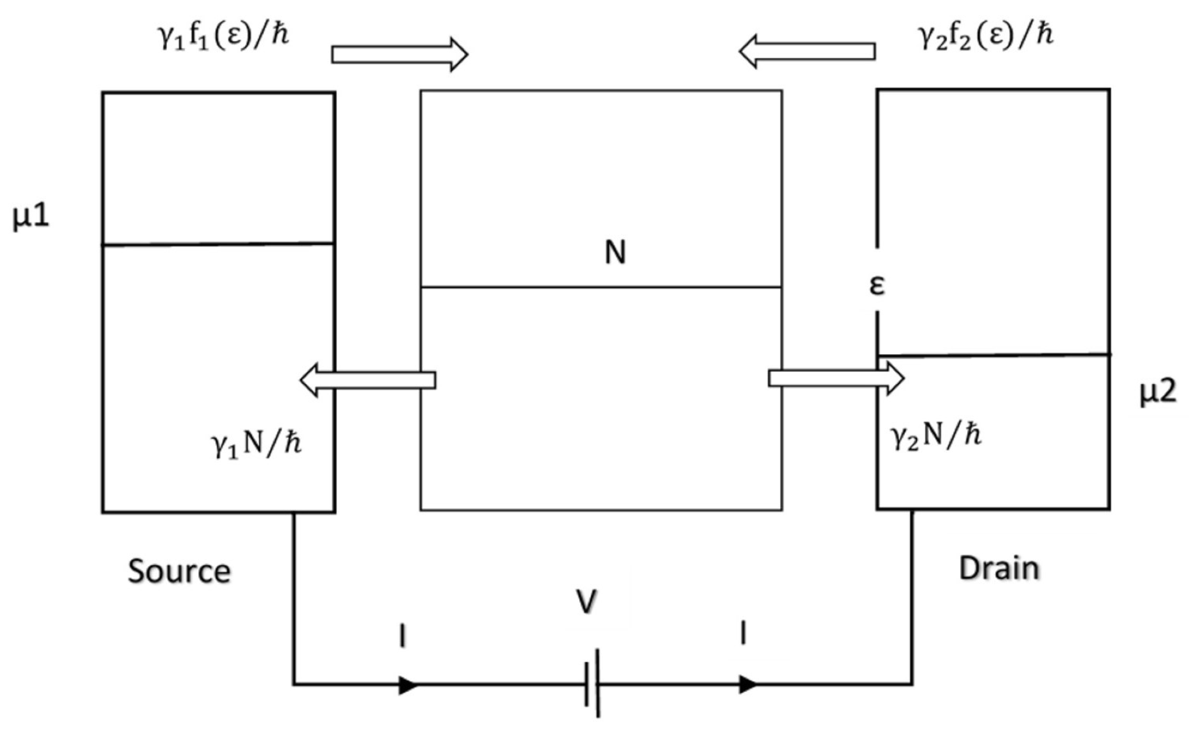
To comprehend the current flow at the source and the drain, we consider a single-level device and its corresponding rate equations, as illustrated in Figure 2.
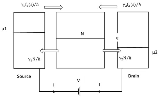
Figure 2.
One-level device. Fermi levels and picturized rate equations.
The current flows into and out of the source and drain ends, characterized by Fermi levels and for the source and the drain, respectively. It is important to note that energy lies between the Fermi levels in the two contacts. The Fermi functions of the source and the drain, denoted as and , respectively [28], indicate that at the source, electrons occupy the corresponding state, and at the drain, electrons occupy this state. The average number of electrons is represented by N.
To provide a more precise description of the electron flow between the contacts, our classical approach incorporates the quantum of conductance. When small voltage is applied to this device, the Fermi energies of the source and drain become split. Initially, before the channel couples with the source and the drain, one level exists in the channel while both the source and the drain maintain a continuous distribution of states. Upon coupling, the channel undergoes broadening [28], and this broadening is characterized by a Lorentzian function centered around .
We begin by considering a one-level device with a broadened density of states given by:
where E corresponds to the energy of a specific energy state of the device; is a single discrete energy level; and are the rates at which an electron, placed initially at level , will escape into the source and drain contacts, respectively, and is given by:
The current is given by
where q is the charge per electron; ; h is Planck’s constant; U is the total potential energy and is given by
where is the gate capacitance; is the drain capacitance; is the total capacitance [28,29] and is given by
where is the source capacitance.
In Equation (3), and are the Fermi distributions functions for source and drain, respectively [30], as mentioned before. The term in Equation (4) expresses the change in the number of electrons and is calculated with respect to the reference number of electrons, originally in the channel, corresponding to which its energy level ε is known [28].
Initially, we assume that / = 0.25 eV, = = 0.005 eV, = 0.2 eV, gate voltage = 0 V, = 0.025 eV where is the Boltzmann constant and T is the absolute temperature, / = 0.5. It is anticipated that the current will increase when the applied drain voltage becomes sufficiently large, causing the energy level to fall within the energy window between Fermi levels and , as illustrated in Figure 2.
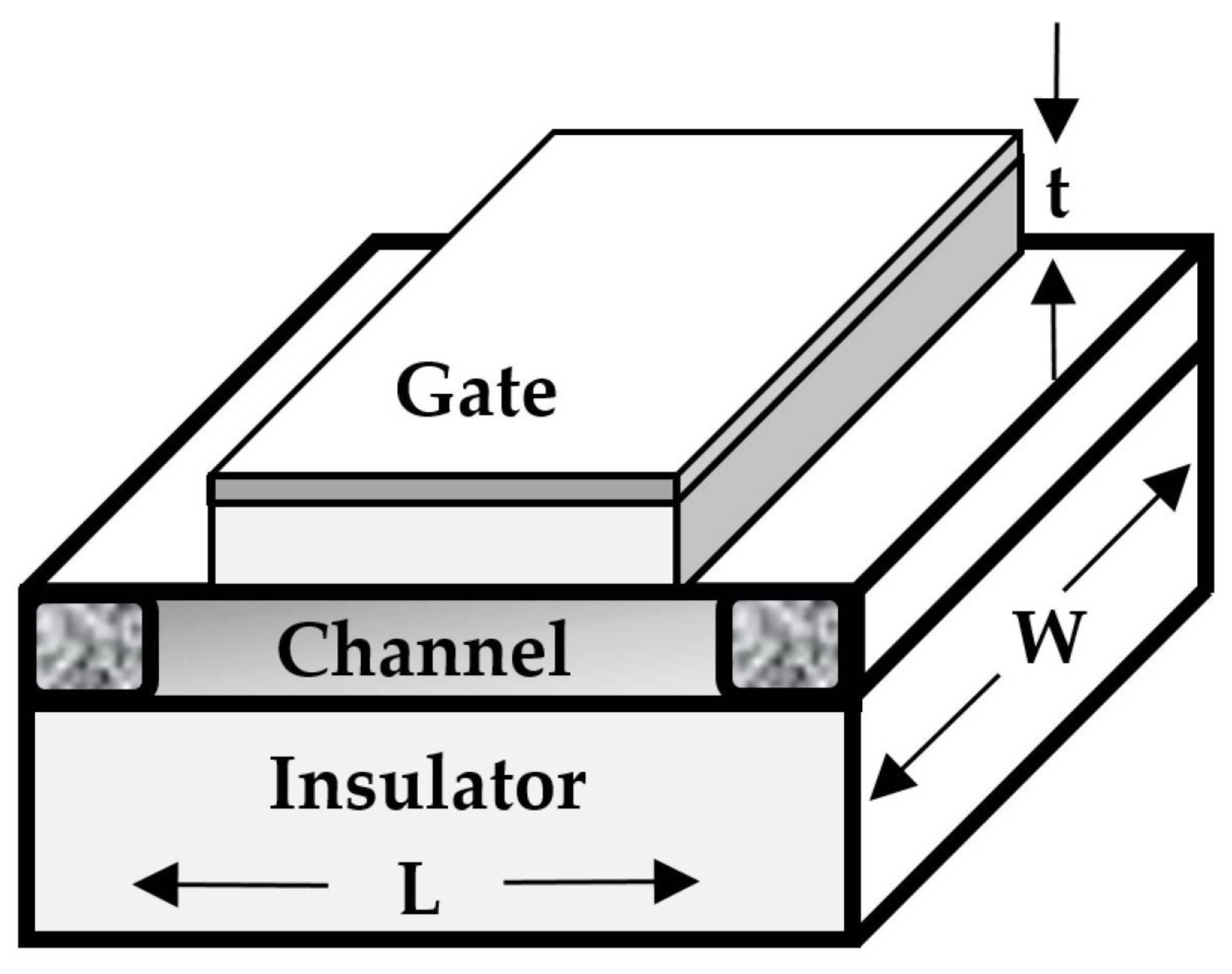
If we set = 0.005 eV for > 0 and = 0.0 eV for < 0, then the current–voltage characteristic needs parametric investigation. In our assumptions, is independent of energy and equal to 0.005 eV [28]. First of all, we study the electrical behavior of Single-Electron Transistors and we investigate the influence of gate voltage values in - curves. The parameters are = −0.2 eV, = , , W = 1 µm, L = 10 nm (W and L are the transistor’s dimensions; see Figure 3), insulator thickness t = 1.5 nm [30], where = 4 is the dielectric constant; is the electrical permittivity of the vacuum. In Figure 3, the corresponding structure of the physical layers of a typical SET is presented. The correspondence to the presented SET schematic structure of Figure 1 is evident.
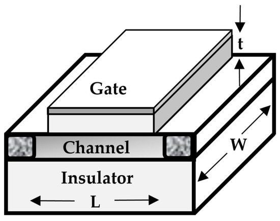
Figure 3.
The typical physical layer structure of an SET, corresponding to the schematic structure appearing in Figure 1.
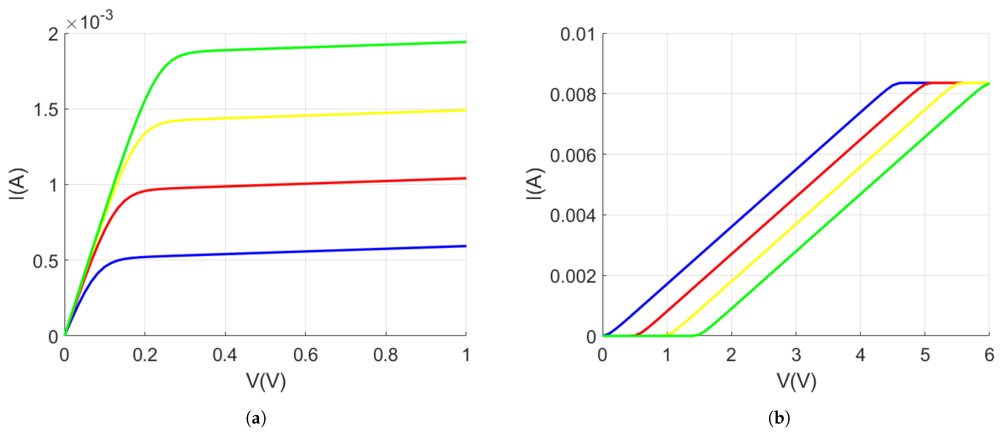
In Figure 4a,b, the SET - curves under forward bias conditions unveil intriguing insights into the behavior of the device, particularly under the influence of positive gate voltage () values. Figure 4a elucidates a noteworthy progression, wherein current experiences a linear upswing with the drain–source voltage () as values increase, even at lower voltage levels. This linear trend persists until a critical threshold is reached, beyond which the current saturates. Notably, the saturation value of drain–source voltage , marking the point of current saturation, escalates proportionally with positive gate voltage , reaching higher positive magnitudes. Concurrently, the saturation current value exhibits a corresponding increase.
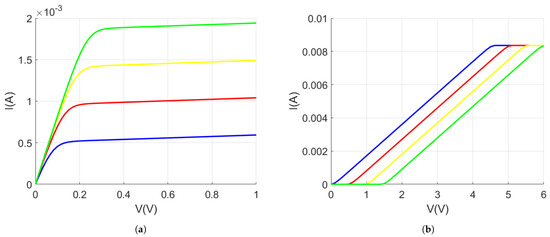
Figure 4.
SET - curves (I and V on the graph axes) under forward bias conditions. (a) Blue line corresponds to = 0.5 V, red line = 0.75 V, yellow line = 1 V, green line = 1.25 V. A typical transistor behavior is illustrated. (b) SET - curves under forward bias conditions for higher gate voltage; blue line corresponds to = 8.5 V, red line to = 0.9 V, yellow line to = 9.5 V, green line to = 10 V. All characteristics saturate to the same drain current level.
As positive gate voltage continues to escalate, Figure 4a indicates that current maintains a relatively low level, initiating a subsequent linear rise with after surpassing a discernible threshold. Significantly, this threshold value demonstrates an elevation in tandem with increasing , eventually leading to another common saturation point, as illustrated in Figure 4b.
The observed behavior, where current surges with increasing positive gate voltage , can be attributed to the positively charged gate. The presence of positive charges on the gate attracts electrons of intrinsic conductivity within the p-channel, augmenting the carrier concentration in the channel. With each incremental increase in , the electron concentration further intensifies, resulting in a notable reduction in channel resistance. This reduction in resistance is pivotal, contributing to the observed increase in current through the device, particularly for specific values of drain–source voltage .
This intricate interplay between and the device’s electrical characteristics highlights the impact of positive gate voltage on carrier concentration, channel resistance, and ultimately the overall current flow through the device. A deeper exploration of these phenomena promises valuable insights into the device’s functionality and may pave the way for optimized applications in electronic systems.
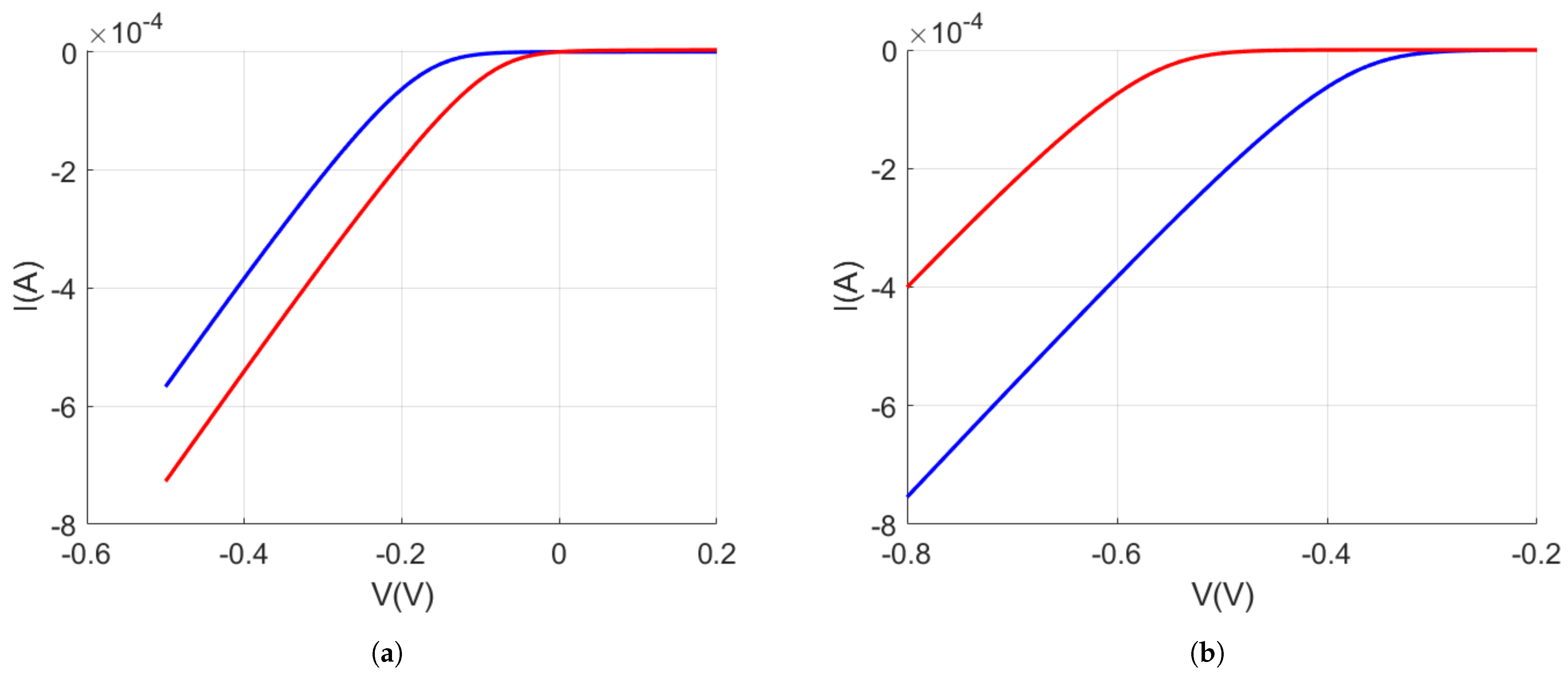
In Figure 5a and Figure 4b, the reverse bias characteristics of the device are elucidated through the SET - curves for positive and negative gate voltage () values, correspondingly. Figure 5a unveils a distinct trend as increases to higher positive values, where current flowing through the device initiates a linear rise with negative drain–source voltage () after surpassing a discernible threshold. Notably, this threshold value exhibits an increase in tandem with the applied gate voltage, .
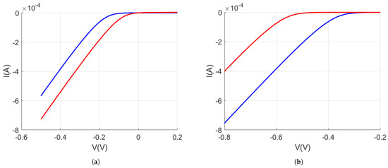
Figure 5.
(a) - curves in reverse bias for different positive gate voltage values . Blue line, = 0.01 V; red line, = 0.1 V. (b) - curves in reverse bias for different negative gate voltage values . Blue line, = −0.2 V; red line, = −0.4 V.
A parallel behavior is observed in Figure 5b, where - curves in reverse bias for negative values are presented. Here, current for specific values escalates as takes higher negative values. Intriguingly, unlike the positive scenario, the threshold value of , beyond which the current rises linearly, remains unaffected by . This behavior is indicative of the intricate influence of gate voltage polarity on the device’s electrical characteristics. In Figure 5a, the positive gate voltage attracts carriers, resulting in an increased electron concentration in the channel, leading to the observed linear rise in current with negative . The fact that the threshold value increases with suggests a nuanced interplay between gate voltage and the initiation of this linear rise.
Similarly, in Figure 5b, the negative gate voltage induces a rise in current for specific values, indicating the significance of carrier dynamics under negative conditions. However, the consistent threshold value of implies that, unlike the positive scenario, the initiation of the linear rise in current is not affected by the magnitude of negative gate voltage.
These findings underscore the polarity-dependent response of the device to gate voltage variations in reverse bias conditions. Further exploration and analysis of these behaviors hold promise for a comprehensive understanding of the device’s characteristics, paving the way for tailored applications in electronic systems.
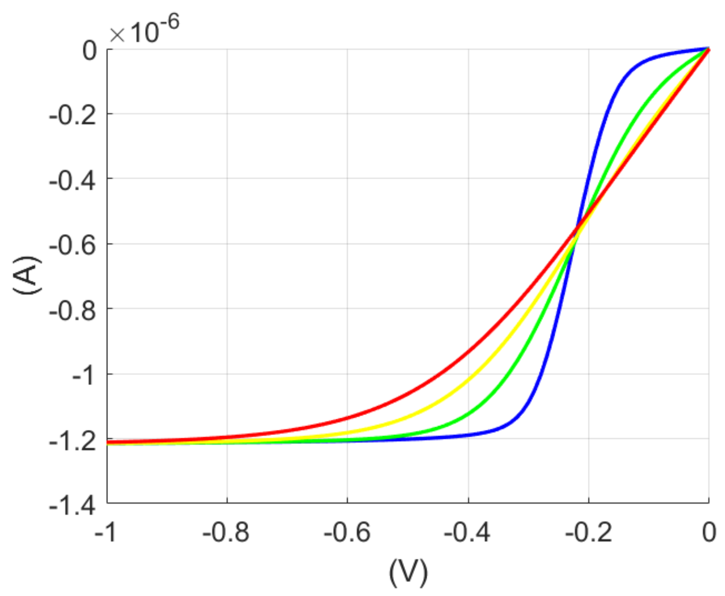
The impact of temperature (T) on the electrical behavior of the Single-Electron Transistor (SET) is further elucidated in Figure 6, which provides an overview of - curves with gate voltage held at 0 V. Across all temperatures, a distinctive N-type negative differential resistance (NDR) region becomes apparent in the - curves. This intriguing effect stems from the enhancement of one of the two tunneling barriers within the transistor, facilitated by the source–drain electric field.
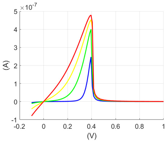
Figure 6.
Temperature T effect in SET’s - curves. Blue line, T = 100 K; green line, T = 300 K; yellow line, T = 500 K; red line, T = 700 K.
Notably, the temperature-dependent behavior is highlighted in Figure 6, where it is evident that the value of at which the negative differential resistance region manifests undergoes modifications with changes in temperature. Specifically, with an increase in temperature (T), the critical value (where NDR appears) takes on lower positive magnitudes. This observation underscores the dynamic influence of thermal energy on the tunneling processes within the transistor, shaping its electrical characteristics.
Furthermore, Figure 6 reveals that as the temperature rises, the value of the current’s peak also increases. This temperature-dependent enhancement in the current’s peak further adds to the complexity of the N-type NDR phenomenon. It is noteworthy that this behavior is not only inherent in a variety of materials [30] but is also observed at the atomic level [31].
Figure 7 presents - temperature dependence at reverse bias. It is clear that the N-type NDR region is not present at this temperature range.
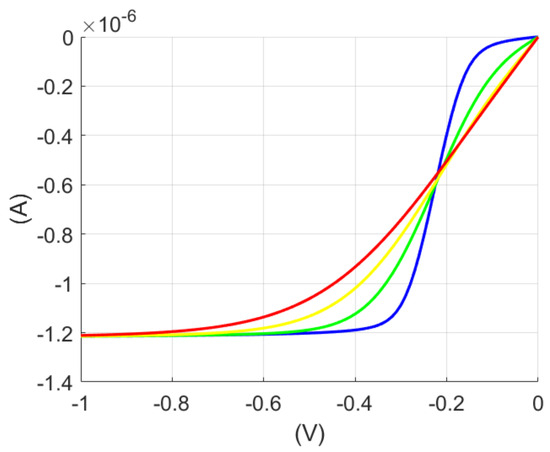
Figure 7.
- temperature dependence at reverse bias. Blue line, T = 100 K; green line, T = 300 K; yellow line, T = 500 K; red line, T = 700 K.
In summary, the intricate interplay between temperature, tunneling barriers, and the resulting N-type NDR phenomenon is elucidated through detailed - curves. This deeper understanding may open avenues for temperature-sensitive applications and optimizations in electronic systems employing SET configurations.
In the realm of fabricated nanoelectronic devices [32], analog results have been meticulously observed and recorded. The intriguing influence of temperature on these devices aligns with a model simulation akin to the Fermi Golden Rule [33]. In an experiment where temperature T is held constant at an extremely low value of 0.025 K (almost zero, 0 K), variations in gate voltage values unveil a compelling phenomenon: as ascends from 0 V to 10 V, the characteristic N-type negative differential resistance region in the - curves diminishes, and begins to rise at higher .
This distinctive behavior, vividly illustrated in Figure 8a,b, delineates the impact of negative gate voltage values on the N-type negative differential resistance region, a phenomenon previously documented [13]. Notably, as takes on progressively higher negative values, the region of N-type negative differential resistance gradually fades, and the - curves transform into the typical - curves of a symmetric SET junction.
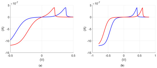
Figure 8.
(a) - curves for different positive gate voltage and constant temperature T values. Blue line, = 0.01 V; red line, = 0.1 V. (b) - curves for different negative gate voltage and constant temperature T values. Blue line, = −0.01 V; red line, = −0.1 V.
This insightful observation underscores the pivotal role of negative gate voltages in modulating the electrical characteristics of the fabricated nanoelectronic device. The disappearance of the N-type negative differential resistance region and the transition to symmetric - curves reveal the nuanced influence of gate voltage polarity on the tunneling processes and overall behavior of the SET junction.
The findings not only corroborate experimental results, but also contribute to a deeper understanding of how gate voltage variations, especially in the negative range, can be leveraged to manipulate the electrical response of nanoelectronic devices. Such insights may prove instrumental in the design and optimization of SET-based circuits and systems for various applications in nanoelectronics.
4. Discussion
The acknowledgment that the operation of Single-Electron Transistors (SETs) involves pure quantum mechanical processes and surpasses classical models is crucial in understanding their intricate behaviors. While classical models, including the one presented in this study involving broadening functions and Landauer’s formula, may not capture the full quantum complexity, they offer valuable insights into the impact of external parameters such as temperature on the Negative Differential Resistance (NDR) effect.
The inclusion of a Lorenzian density of states broadening discrete level ε is a significant aspect of the model. Acknowledging the existence of multiple levels, even though only one independent level is studied, is essential. This recognition prompts consideration of Coulomb oscillations arising from these multilevels, which can profoundly affect the I-V characteristics of the SET.
The study reveals that the NDR effect of an SET is intricately tunable by both temperature and drain–source voltage. As the temperature escalates from 0 K to room temperature, the emergence of N-type negative differential resistance becomes evident at lower drain–source voltage values. Simultaneously, the choice of gate voltage () exhibits an opposite effect on the N-type negative differential resistance behavior.
An essential outcome is the realization that, with a judicious selection of temperature and gate voltage, a Single-Electron Transistor can manifest diverse behaviors, ranging from negative differential resistance to typical on–off transistor behavior or simple resistance behavior. This heightened controllability positions the SET as a highly versatile and manipulable nanodevice.
The appearance, form, and potential hysteresis effect of NDR make the SET an ideal candidate for applications in negistor and memristive devices. The intricacies unveiled in this study not only contribute to a better understanding of SET behavior, but also open avenues for exploiting these nanodevices in emerging technologies with implications for computing, memory, and beyond. Further research and exploration in this direction promise to unveil even more sophisticated and nuanced functionalities of Single-Electron Transistors.
The intricacies uncovered in this study lay the foundation for deeper exploration into the potential applications and further refinement of the control mechanisms of Single-Electron Transistors (SETs). The dynamic interplay between temperature, gate voltage, and the resulting I-V characteristics introduces a spectrum of possibilities for tailoring the behavior of these nanodevices.
The acknowledgment that the model explores only one independent level, while there may be multiple discrete levels, prompts a more comprehensive examination. Future research could delve into the impact of these multilevel structures on Coulomb oscillations and how they collectively contribute to the overall performance of SETs. Understanding and controlling these oscillations could provide a pathway for even finer control over device behavior. Expanding on the idea of tuning the NDR effect through temperature and gate voltage, researchers may explore optimization strategies. Investigating specific temperature and gate voltage combinations that yield desired behaviors could pave the way for tailored applications. This optimization could be crucial for achieving reliable and reproducible outcomes in practical applications.
The controllability demonstrated in the study positions SETs as promising candidates for various emerging technologies. Beyond negistor and memristive applications, SETs could find applications in quantum computing, neuromorphic computing, and other advanced computational paradigms. The ability to manipulate their behavior with external parameters makes them adaptable to diverse requirements. The observed hysteresis effects in the NDR behavior of SETs introduce interesting possibilities for memory applications. Investigating the characteristics of this hysteresis, such as its dependence on temperature and gate voltage, could pave the way for developing robust and energy-efficient memory devices. This could be particularly valuable in the era of low-power and high-density memory solutions.
While the theoretical model and simulations provide valuable insights, experimental validation is essential. Researchers should consider translating these findings into practical experiments, fabricating SET devices with the suggested parameters, and empirically confirming the predicted behaviors. This step is crucial for bridging the gap between theoretical studies and real-world applications. The study’s findings have implications for the design of nanoelectronic circuits. Engineers and designers may leverage the controllability of SETs to enhance the performance and functionality of circuits at the nanoscale. The integration of SETs into existing or novel circuit architectures could lead to advancements in computational efficiency and energy consumption.
In conclusion, the study’s insights into the temperature-dependent behaviors of Single-Electron Transistors open up a rich landscape for exploration and application. By refining theoretical models, optimizing external parameters, and bridging the gap between theory and experimentation, researchers can unlock the full potential of SETs for transformative contributions to the field of nanoelectronics. The journey toward harnessing the quantum mechanical intricacies of SETs is poised to bring about paradigm-shifting advancements in technology.
5. Conclusions
In conclusion, the study delving into the temperature-dependent behaviors of Single-Electron Transistors (SETs) reveals a profound interplay between quantum mechanical processes and external parameters. While the pure quantum nature of SET operations defies classical models, the presented model incorporating broadening functions, Landauer’s formula, and Lorenzian density of states proves instrumental in describing the influence of temperature on the Negative Differential Resistance (NDR) effect. The recognition of the existence of multiple discrete energy levels prompts a comprehensive examination, hinting at the potential contribution of these multilevel structures to Coulomb oscillations and their collective impact on the SET’s current–voltage (I-V) characteristics. This not only expands our theoretical understanding but also opens avenues for further exploration into the nuanced behaviors of SETs. The controllability demonstrated through the manipulation of temperature and gate voltage positions SETs as highly adaptable nanodevices. The emergence of N-type negative differential resistance with increasing temperature, coupled with the opposite effect influenced by gate voltage values, emphasizes the intricate tunability of these devices. The study highlights that, with a judicious selection of these parameters, SETs can exhibit a spectrum of behaviors ranging from negative differential resistance to traditional transistor behavior and simple resistance. This controllability marks SETs as versatile and finely tunable platforms, offering possibilities for tailored applications.
Importantly, the study identifies SETs as ideal candidates for negistor and memristive applications. The observed hysteresis effects and the adaptability to external parameters make SETs promising for emerging technologies, including quantum computing and neuromorphic computing. Beyond theoretical exploration, the study emphasizes the need for experimental validation to bridge the gap between theory and real-world applications.
In the broader context, the insights gleaned from this research not only contribute to our understanding of nanoscale electronics but also hold significant implications for the design of nanoelectronic circuits. The controllability of SETs opens new possibilities for enhancing the performance and functionality of circuits at the nanoscale, potentially leading to advancements in computational efficiency and energy consumption. As we navigate the quantum landscape of SETs, this study serves as a cornerstone, providing a roadmap for future research endeavors. The journey toward harnessing the full potential of SETs in the realm of nanoelectronics is poised to bring about transformative advancements, and this work paves the way for continued exploration into the rich and intricate behaviors of these quantum devices.
Author Contributions
All of the authors made significant contributions to this work. Methodology, P.P. and M.P.H.; software, P.P.; validation, K.O. and E.P.; formal analysis, L.M. and S.G.S.; investigation, P.P.; resources, K.O.; writing—original draft preparation, P.P. and E.P.; writing—review and editing, S.G.S. and K.O.; visualization, S.G.S.; supervision, L.M. All authors have read and agreed to the published version of the manuscript.
Funding
This research received no external funding.
Data Availability Statement
Data are contained within the article.
Conflicts of Interest
The authors declare no conflicts of interest.
References
- Touati, A.; Chatbouri, S.; Adel, K. Design of a single-electron memory operating at room temperature. Int. Sch. Res. Not. 2013, 2013, 587436. [Google Scholar] [CrossRef]
- Zardalidis, G.T.; Karafyllidis, I. Design and simulation of a nanoelectronic single-electron control—Not gate. Microelectron. J. 2006, 37, 94–97. [Google Scholar] [CrossRef]
- Hosseini, V.K.; Ahmadi, M.T.; Afrang, S.; Ismail, R. Analysis and simulation of coulomb blockade and coulomb diamonds in fullerene single electron transistors. J. Nanoelectron. Optoelectron. 2018, 13, 138–143. [Google Scholar] [CrossRef]
- Chouvaev, D.; Kuzmin, L.; Golubev, D.; Zaikin, A. Coulomb blockade in a SET transistor and a single tunnel junction: Langevin equation approach. Phys. B Condens. Matter 2000, 284, 1786–1787. [Google Scholar] [CrossRef]
- Kumar, O.; Kaur, M. Single electron transistor: Applications & problems. Int. J. VLSI Des. Commun. Syst. (VLSICS) 2010, 1, 24–29. [Google Scholar]
- Sinha, P.K.; Sanjay, S. Single electron transistor and its simulation methods. Int. J. Eng. Dev. Res. 2014, 2, 1907–1925. [Google Scholar]
- George, H.C.; Pierre, M.; Jehl, X.; Orlov, A.O.; Sanquer, M.; Snider, G.L. Application of negative differential conductance in Al/AlOx single-electron transistors for background charge characterization. Appl. Phys. Lett. 2010, 96, 042114. [Google Scholar] [CrossRef]
- Kaasbjerg, K.; Flensberg, K. Image charge effects in single-molecule junctions: Breaking of symmetries and negative-differential resistance in a benzene single-electron transistor. Phys. Rev. B 2011, 84, 115457. [Google Scholar] [CrossRef]
- Miyaji, K.; Saitoh, M.; Hiramoto, T. Compact analytical model for room-temperature-operating silicon single-electron transistors with discrete quantum energy levels. IEEE Trans. Nanotechnol. 2006, 5, 167–173. [Google Scholar] [CrossRef]
- Aminzadeh, H.; Dashti, M.A.; Miralaei, M. Nano-scale silicon quantum dot-based single-electron transistors and their application to design of analog-to-digital convertors at room temperature. J. Circuits Syst. Comput. 2017, 26, 1750201. [Google Scholar] [CrossRef]
- Chen, X.; Xing, Z.; Sui, B. Tunable Negative Differential Resistance of Single-Electron Transistor Controlled by Capacitance. In Computer Engineering and Technology, Proceedings of the 17th CCF Conference, NCCET 2013, Xining, China, 20–22 July 2013; Revised Selected Papers 17; Springer: Berlin/Heidelberg, Germany, 2013; pp. 228–234. [Google Scholar]
- Sée, J.; Dollfus, P.; Galdin, S.; Hesto, P. Negative differential conductance in silicon nanocrystal single-electron devices. In Proceedings of the 30th European Solid-State Circuits Conference (IEEE Cat. No. 04EX850), Leuven, Belgium, 23 September 2004; pp. 433–436. [Google Scholar]
- Sui, B.; Fang, L.; Chi, Y.; Zhang, C. Analysis of negative differential conductance of single-island single-electron transistors owing to Coulomb oscillations. IET Circuits Devices Syst. 2010, 4, 425–432. [Google Scholar] [CrossRef]
- Weaver, R.; Lobkis, O.; Yamilov, A. Entrainment and stimulated emission of ultrasonic piezoelectric auto-oscillators. J. Acoust. Soc. Am. 2007, 122, 3409–3418. [Google Scholar] [CrossRef]
- Kuzmin, L.; Pashkin, Y.A.; Tavkhelidze, A.; Ahlers, F.J.; Weimann, T.; Quenter, D.; Niemeyer, J. An all-chromium single electron transistor: A possible new element of single electronics. Appl. Phys. Lett. 1996, 68, 2902–2904. [Google Scholar] [CrossRef]
- Gibson, G.A. Designing Negative Differential Resistance Devices Based on Self-Heating. Adv. Funct. Mater. 2018, 28, 1704175. [Google Scholar] [CrossRef]
- Livermore, C. Coulomb Blockade Spectroscopy of Tunnel-Coupled Quantum Dots; Harvard University: Cambridge, MA, USA, 1998. [Google Scholar]
- Kouwenhoven, L. Single-molecule transistors. Science 1997, 275, 1896–1897. [Google Scholar] [CrossRef]
- Devoret, M.H.; Esteve, D.; Grabert, H.; Ingold, G.L.; Pothier, H.; Urbina, C. Effect of the electromagnetic environment on the Coulomb blockade in ultrasmall tunnel junctions. Phys. Rev. Lett. 1990, 64, 1824. [Google Scholar] [CrossRef] [PubMed]
- Nakamura, Y.; Pashkin, Y.A.; Tsai, J. Coherent control of macroscopic quantum states in a single-Cooper-pair box. Nature 1999, 398, 786–788. [Google Scholar] [CrossRef]
- Zorin, A.; Ahlers, F.J.; Niemeyer, J.; Weimann, T.; Wolf, H.; Krupenin, V.; Lotkhov, S. Background charge noise in metallic single-electron tunneling devices. Phys. Rev. B 1996, 53, 13682. [Google Scholar] [CrossRef] [PubMed]
- Grabert, H.; Devoret, M.H. Single Charge Tunneling: Coulomb Blockade Phenomena in Nanostructures; Springer Science & Business Media: Berlin/Heidelberg, Germany, 2013; Volume 294. [Google Scholar]
- Vion, D.; Aassime, A.; Cottet, A.; Joyez, P.; Pothier, H.; Urbina, C.; Esteve, D.; Devoret, M.H. Manipulating the quantum state of an electrical circuit. Science 2002, 296, 886–889. [Google Scholar] [CrossRef]
- Robertson, J. High k dielectrics for future CMOS devices. ECS Trans. 2009, 19, 579. [Google Scholar] [CrossRef]
- Shakouri, A. Recent developments in semiconductor thermoelectric physics and materials. Annu. Rev. Mater. Res. 2011, 41, 399–431. [Google Scholar] [CrossRef]
- Claeys, C.; Simoen, E. Radiation Effects in Advanced Semiconductor Materials and Devices; Springer Science & Business Media: Berlin/Heidelberg, Germany, 2013; Volume 57. [Google Scholar]
- Snyder, G.J.; Toberer, E.S. Complex thermoelectric materials. Nat. Mater. 2008, 7, 105–114. [Google Scholar] [CrossRef] [PubMed]
- Datta, S. Electrical resistance: An atomistic view. Nanotechnology 2004, 15, S433. [Google Scholar] [CrossRef]
- Hien, D.S.; Thao, H.L.T. Modelling transport in single electron transistor. J. Phys. Conf. Ser. 2009, 187, 012060. [Google Scholar] [CrossRef]
- Pergament, A.; Stefanovich, G.; Malinenko, V.; Velichko, A. Electrical switching in thin film structures based on transition metal oxides. Adv. Condens. Matter Phys. 2015, 2015, 654840. [Google Scholar] [CrossRef]
- Kim, T.K.; Moon, H.R.; Kim, B.H. Symmetric negative differential resistance in a molecular nanosilver chain. J. Nanomater. 2013, 2013, 814694. [Google Scholar] [CrossRef]
- Drouin, D.; Droulers, G.; Labalette, M.; Lee Sang, B.; Harvey-Collard, P.; Souifi, A.; Jeannot, S.; Monfray, S.; Pioro-Ladriere, M.; Ecoffey, S.; et al. A fabrication process for emerging nanoelectronic devices based on oxide tunnel junctions. J. Nanomater. 2017, 2017, 8613571. [Google Scholar] [CrossRef]
- Das, J.C.; De, D.; Debnath, B.; Sarkar, A. Single Layer Design of Dual Banyan Network Using Quantum-Dot Cellular Automata. In Proceedings of the 2023 IEEE Devices for Integrated Circuit (DevIC), Kalyani, India, 7–8 April 2023; pp. 182–185. [Google Scholar]


Disclaimer/Publisher’s Note: The statements, opinions and data contained in all publications are solely those of the individual author(s) and contributor(s) and not of MDPI and/or the editor(s). MDPI and/or the editor(s) disclaim responsibility for any injury to people or property resulting from any ideas, methods, instructions or products referred to in the content. |
© 2024 by the authors. Licensee MDPI, Basel, Switzerland. This article is an open access article distributed under the terms and conditions of the Creative Commons Attribution (CC BY) license (https://creativecommons.org/licenses/by/4.0/).