Abstract
In the realm of Ceph distributed storage systems, ensuring swift and symmetrical data recovery during severe data corruption scenarios is pivotal for data reliability and system stability. This paper introduces an innovative FPGA-based Multi-Dimensional Elastic Recovery Acceleration method, termed AMDER-Ceph. Utilizing FPGA technology, this method is a pioneer in accelerating erasure code data recovery within such systems symmetrically. By harnessing the parallel computing power of FPGAs and optimizing Cauchy matrix binary operations, AMDER-Ceph significantly enhances data recovery speed and efficiency symmetrically. Our evaluations in real-world Ceph environments show that AMDER-Ceph achieves up to 4.84 times faster performance compared with traditional methods, especially evident in the standard 4 MB block size configurations of Ceph systems.
1. Introduction
In the digital era, managing and storing large-scale data has become a critical challenge for enterprises and government sectors [1]. Particularly, with the substantial growth of global data volume and the emergence of various new data application scenarios, data centers must contend with increasing scale and complexity. These challenges have not only heightened the requirements for the stability and security of storage systems but also spurred new technological solutions. In such an environment, erasure coding technology in distributed storage systems has become extremely important due to its outstanding reliability and efficiency [2].
The application of erasure coding technology in distributed environments allows data to be dispersedly stored across multiple servers or storage nodes and protects information from partial node failures by generating redundant data. Compared with traditional data backup and mirroring techniques [3], this method provides a more efficient fault tolerance capability through coded redundancy, enabling erasure codes to adjust their redundancy level according to specific fault tolerance needs, thereby achieving high-level data protection with lower resource consumption [4].
However, in distributed storage environments, despite erasure coding significantly reducing the additional storage requirements due to fault tolerance, it still faces high computational costs and decoding complexity in data recovery, especially when dealing with frequently accessed hot data. Thus, researching how to improve the efficiency of data recovery in distributed erasure-coded storage systems has become an important issue. Among the many types of erasure codes, Reed–Solomon (RS) erasure codes, as a foundational technology widely used in distributed storage systems, play a decisive role in enhancing the efficiency of data recovery, impacting the performance and reliability of the entire system [5].
Current research has improved the efficiency of erasure codes in data recovery in several ways, focusing on encoding design, network transmission optimization, and decoding acceleration. With continuous breakthroughs in encoding design and the application of high-performance network technologies such as InfiniBand and RDMA in storage systems [6,7], issues related to encoding design and network bottlenecks have gradually been resolved, making the decoding efficiency of erasure codes a key factor affecting data recovery efficiency.
First, in the field of encoding design, concepts like Regeneration codes proposed by Dimakis et al. [8] aim to minimize recovery bandwidth and storage overhead. Huang and his team [9] developed Local Reconstruction Codes (LRCs) by grouping encoded data blocks and creating local redundancy blocks, significantly improving the recovery efficiency of data within groups. After years of development, LRC has seen many mature encodings [10,11,12].
Second, in terms of network transmission optimization, innovative methods have been proposed. For example, Shen et al. [13] introduced a cluster-aware scattered recovery method called ClusterSR, which reduces cross-cluster recovery traffic and increases recovery throughput. Zhou et al. [14] proposed two recovery techniques, SMFRepair and MSRepair, aimed at optimizing auxiliary node selection and utilizing idle nodes to bypass low-bandwidth links, improving the fault recovery performance based on Reed–Solomon coding in heterogeneous networks. Hou’s research team [15] introduced an erasure code family called Rack-Aware Regeneration Codes (RRCs), achieving the optimal solution for this trade-off.
Lastly, in the field of decoding acceleration, PPR [16] adopts hierarchical decoding, partially parallelizing the recovery process; Li et al. [17] proposed a pipeline-based RP method, decomposing recovery operations into multiple parallel sub-operations and precisely scheduling recovery traffic. Plank et al.’s ISA-L acceleration library [18] significantly improved the speed of finite field multiplication for RS erasure codes, thereby greatly enhancing data recovery efficiency. Liu et al. [19] designed a GPU-based erasure code library, GCRS, which outperforms the Jerasure library by a factor of ten in performance.
FPGAs (Field-Programmable Gate Arrays) show significant advantages in accelerating storage systems, primarily due to their highly customizable and flexible logic structures, allowing FPGAs to precisely adapt to specific storage operations and algorithms [20]. The high-speed parallel processing capability of FPGAs is particularly suited for accelerating data-intensive tasks, such as erasure code encoding/decoding and matrix operations, while their support for pipeline parallel design significantly improves computational throughput [21]. Moreover, the low demand for memory bandwidth by FPGAs enables a more efficient use of existing resources without additional costs. Their dynamic reconfiguration and reprogramming capabilities further reduce hardware costs and provide better adaptability [22]. Therefore, FPGAs play a crucial role in enhancing the processing speed and efficiency of storage systems, especially in high-performance computing and big data environments.
The main contributions of this paper are as follows:
(1) AMDER-Ceph Implementation: This paper introduces the AMDER-Ceph scheme, marking the first use of FPGA technology to accelerate erasure code data recovery in Ceph systems. The scheme effectively integrates Cauchy matrix binary projection, optimized encoding/decoding matrices, and parallel parity and decoding techniques to speed up data recovery at the FPGA level. By leveraging the parallel computing capabilities of FPGAs, this approach significantly reduces data recovery times.
(2) Resilient Recovery under Multiple Block Failures: Addressing multiple block failures, this study presents a multi-dimensional resilient recovery strategy for the Ceph system. It features mechanisms for the rapid identification and restoration of failed blocks, ensuring high efficiency in recovery operations and significantly enhancing system resilience.
(3) Performance Evaluation and Optimization: Performance evaluation tests show that AMDER-Ceph provides substantial performance improvements over Ceph’s native erasure coding plugins, with throughput increases of up to 4.84 times under typical operational configurations. This performance enhancement is particularly notable in the context of Ceph’s default 4 MB data blocks.
The organization of this paper is as follows: Section 2 delves into the fundamental principles of erasure codes and related research on data recovery acceleration. Section 3 details the overall architecture design of the AMDER-Ceph scheme, including Cauchy encoding/decoding matrix design and key technologies such as parallel parity generators and decoders. Section 4 comprehensively evaluates the performance of AMDER-Ceph. Finally, Section 5 concludes and looks forward to future research directions.
2. Background and Related Work
Erasure coding (EC), which originated in the 1960s, is an encoding method designed to enhance the fault tolerance of data transmission [23]. Initially developed to address data loss issues during network transmission in the communications field [24], its core idea involves subdividing the transmission signal and incorporating a verification mechanism, thereby creating interconnections among the signals. A notable characteristic is that even if part of the signal is lost during transmission, the receiving end can still reconstruct the complete information content using this algorithm. In today’s era, erasure coding technology is widely applied in the field of distributed storage systems [25].
Erasure codes are primarily divided into three categories: array codes (such as RAID5, RAID6), Reed–Solomon (RS) erasure codes, and Low-Density Parity Check Codes (LDPCs) [26]. The operational process of this technology first involves segmenting the original data, followed by encoding based on these data segments to generate corresponding backup data. Ultimately, the system stores both the original and backup data in different storage media. The data recovery process in erasure coding is essentially the inverse operation of encoding, requiring that the matrices used for encoding are invertible. Therefore, this process is also often referred to as decoding.
2.1. Finite Fields
Finite fields, also known as Galois fields, are a mathematical concept proposed by Évariste Galois in the early 19th century for the study of solutions to algebraic equations [27]. These fields have widespread applications in cryptography, coding theory, computer science, and combinatorial mathematics. In abstract algebra, a field F is defined as a set closed under basic operations (addition, subtraction, multiplication, and division), where each element must have an additive inverse and a multiplicative inverse, and every non-zero element must have a multiplicative identity. If the number of elements in field F is finite, then the field is defined as a finite field. The structure and properties of these fields play a key role in understanding and solving various mathematical and engineering problems [28].
Generally speaking, the order of a finite field refers to the total number of elements it contains, and it is always in the form of a power of a prime number p raised to n, denoted as , for example, finite fields of order or . Finite fields are commonly represented as , where GF stands for Galois field, p is the prime base, and n is the highest degree of polynomials in that field. In , each element can be represented as a polynomial of degree less than n, with coefficients from the smaller field . Moreover, forms an n-dimensional linear space over , with a basis consisting of a set of n-th degree polynomials , thereby allowing every element in to be represented as a linear combination of these basis elements. For instance, is a field containing eight elements, constituted by the third power of the prime number 2. In this field, each element can be represented as a polynomial of degree less than 3 over , where contains two elements . For example, a specific element might be expressed as , where take values from , that is, either 0 or 1. Therefore, possible elements include and , etc.
In the finite field , the additive identity is defined as 0, while the multiplicative identity is 1. For any element a in the field, its additive inverse is defined as , such that . Similarly, for any non-zero element b, its multiplicative inverse satisfies . All addition and subtraction operations in this field follow modulo p arithmetic, i.e., and . Multiplication and division also follow the same modulo p arithmetic, respectively represented as and .
In particular, when , i.e., for the field , addition and subtraction operations are equivalent to the XOR operation. For example, in , the operation is equivalent to in binary, resulting in 0. At this point, elements in the field can be represented as binary numbers; for instance, the polynomial corresponds to the binary number . Due to the widespread use of binary numbers in computers, is particularly important in cryptography, as it corresponds to 8-bit binary numbers (i.e., 1 byte).
Furthermore, the concept of a generator in finite fields is crucial for understanding the structure of the field. A generator is a special element in the field whose powers can generate all non-zero elements of the field. In the field , the number 2 often acts as a generator. For example, in , considering 2 as a generator, its powers will generate all non-zero elements of the field, such as , up to . These elements can be represented as polynomials in and presented in the form of three-digit binary numbers.
In the finite field , the application of the polynomial generator g is a core concept. Any element a can be expressed as , where k is the exponent. Taking as an example, this field contains 16 elements, generated by the primitive polynomial , with the other 14 elements generated by this polynomial. In this context, since g cannot generate the polynomial 0, there exists a cyclic period, which is . Thus, when , k can be simplified as . Table 1 shows the relationship between the generated elements of GF(24) and their corresponding polynomial, binary, and decimal representations.

Table 1.
GF(24) generated elements and their polynomial, binary, and decimal representations.
In the GF(2w) field, multiplication operations can be simplified to addition operations. Specifically, if and , then the following holds true:
Using a lookup table method, one can find the corresponding n and m values for a and b, respectively, and then calculate . Moreover, the relationship between elements in the field and their exponents can be constructed and utilized through forward and reverse lookup tables. In the context of GF(24), these tables are referred to as gflog and gfilog, used for mapping binary forms to polynomial forms, and vice versa. Table 2 is the forward and reverse table of exponents and logarithms for .
Table 2.
Table of exponents and logarithms for elements of GF(24).
For example, in GF(24), multiplication and division calculations can be performed according to Equations (2) and (3).
Specific examples include the following:
and
Through this method, computational efficiency is significantly improved, which can be quantified by algorithm complexity theory. Specifically, unoptimized direct multiplication or division typically involves polynomial multiplication or finding the multiplicative inverse, with an algorithm complexity of polynomial level, denoted as , where n represents the size of the operands, and k is a constant greater than 1. Conversely, the multiplication and division using the lookup table method primarily rely on lookup operations and simple addition or subtraction, both with a constant time complexity of . Therefore, the overall time complexity of the lookup table method is also . The efficiency of this method becomes particularly significant when dealing with large-scale data, significantly reducing the original polynomial time complexity to constant time complexity, thus achieving a substantial improvement in computational efficiency.
2.2. Cauchy Reed–Solomon Codes
Reed–Solomon (RS) encoding, based on finite field arithmetic, is a type of error-correcting code widely used in data communications and storage systems, such as CDs, wireless communications, and data center storage. It can correct or recover errors caused by noise, data corruption, or loss [29]. In RS encoding, given k data blocks , the encoding process involves generating m additional parity blocks , forming an RS code, where . This coding method is particularly suited for fault tolerance because it can recover the original data from any k blocks out of the n original and parity blocks.
A key step in RS encoding is constructing an encoding matrix . This matrix contains the coefficients used to generate parity blocks, and its design must ensure that the vectors in the matrix are linearly independent, meaning that any combination of m rows can generate an m-dimensional space. This ensures that the rank . By calculating Equation (4), we obtain the parity blocks P, which are stored or transmitted along with the original data blocks for subsequent error detection and correction.
Decoding in RS encoding is a complex process that involves recovering the original information from the received data blocks. With at most m data or parity blocks lost, decoding requires at least k data or parity blocks. This process typically involves constructing a new decoding matrix , which is extracted from the original encoding matrix and the identity matrix I. By calculating Equation (5) (where is the selected k blocks), the original data D can be recovered. This process requires the inverse matrix of to exist, which is a condition that RS encoding design must satisfy.
Next, we prove the invertibility of the selection matrix. For an Cauchy matrix, it is defined as follows: Let A and B be two sets of elements in the finite field GF(2w), , , for all , all , with , and no repeated elements in sets A and B. The construction of the Cauchy matrix is shown in the following Equation (6):
First, we multiply row i of matrix X by , and the original expression can be written as , where is an n-order determinant, its element being . We intuitively look at the following Equation (7):
It is noted that if , then two rows are the same; if , then two columns are the same. Therefore, , implying that contains factors , . In the expansion of , appear times, as shown in the following Equation (8):
To determine the value of k, let , noting that, except for elements on row i and column i, all other elements are 0, making it a diagonal determinant, the value being the product of the main diagonal elements. At this time, , where , showing that . Thus, Equation (9) can be derived as follows:
For an n-order Cauchy matrix, as long as , the determinant of the matrix is non-zero and greater than 0, thereby ensuring the matrix’s invertibility. More importantly, any m-order submatrix () of the Cauchy matrix also satisfies the conditions of non-zero determinant and invertibility, providing assurance for the matrix’s applicability and flexibility.
Additionally, it is worth noting that standard RS encoding may require expensive computations during decoding, especially when solving the inverse matrix. To optimize this process, Cauchy RS encoding was proposed. Initially, Cauchy RS encoding [30] replaced traditional Vandermonde RS encoding, solving the problem of high computational complexity of inverse operations, reducing it from to . This improvement significantly speeds up the decoding process, especially in applications dealing with large volumes of data. Subsequently, Cauchy RS encoding employs binary representation in the finite field GF(2w), simplifying multiplication operations to efficient XOR operations, further reducing computational complexity and enhancing processing speed. Finally, by applying optimized Cauchy RS encoding to FPGA (Field-Programmable Gate Array) hardware, leveraging its high customizability and support for parallel processing, binary XOR operations can be efficiently implemented in FPGAs, thereby significantly improving throughput and reducing latency in large-scale data processing and high-speed communication systems. These optimization steps not only reflect the evolution of RS encoding theory to practical application but also innovate at each step towards improving encoding and decoding efficiency and reducing computational complexity, enabling RS encoding to more effectively adapt to modern high-speed and large-volume computational environments.
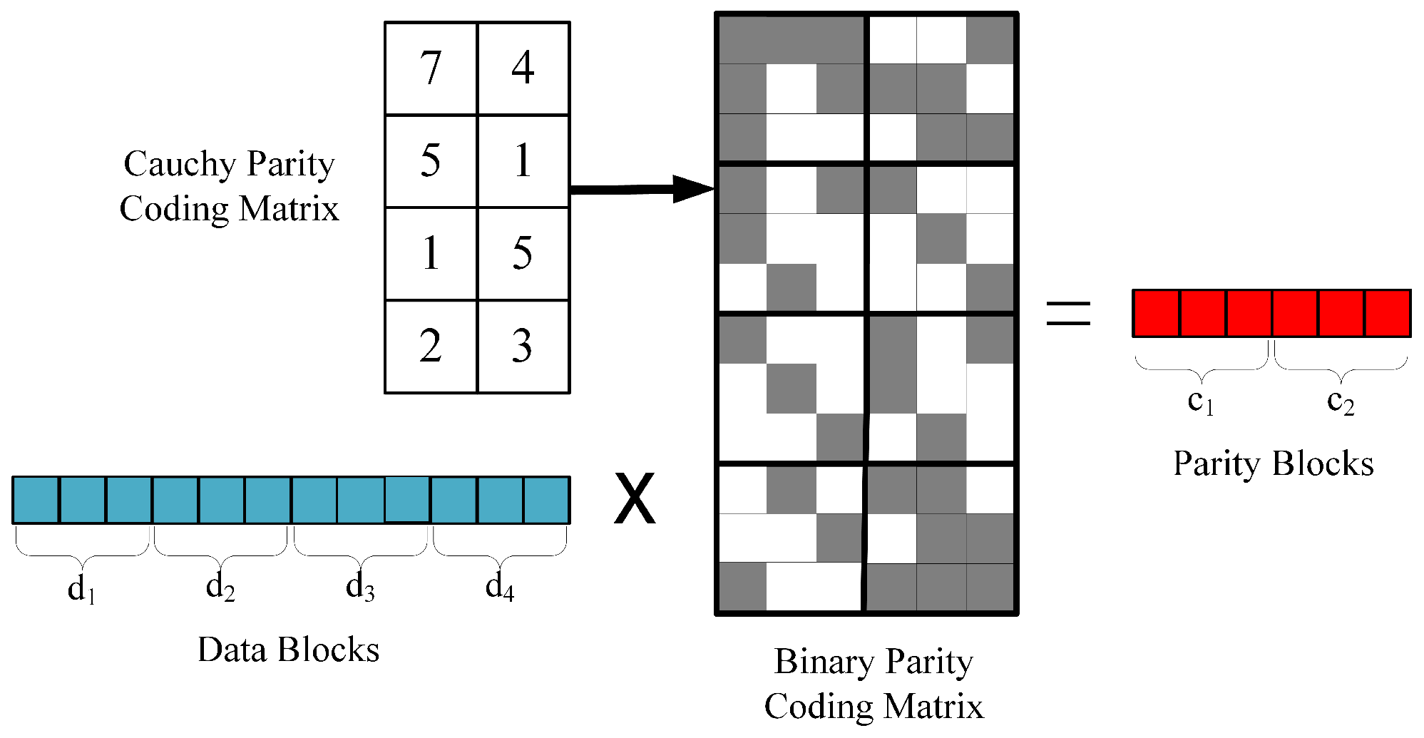
In the scenario depicted in Figure 1, we observe the process of Reed–Solomon (RS) encoding for , , by converting a specific encoding matrix into its binary matrix form. In this binary matrix, gray blocks represent 1, while white blocks represent 0. The encoding operation involves multiplying a 1 × 12 binary vector with a 12 × 6 binary matrix.

Figure 1.
Binary matrix for .
In this process, the computational cost of multiplication mainly depends on the number of 1s (gray blocks) in the binary matrix. According to research by Plank et al. [31], for , optimizing the encoding matrix can reduce the number of 1s in the binary matrix from the original 46 to 34. This optimization significantly reduces the complexity of multiplication operations while maintaining the efficiency and reliability of encoding. This method’s implementation is relatively simple, requiring no additional complex optimization measures, and is an effective way to optimize Reed–Solomon encoding in modern communication and storage systems.
2.3. Acceleration of Data Recovery in Distributed Storage Systems
In distributed storage systems, erasure coding (EC) plays a crucial role, particularly in data recovery. The core challenge of erasure coding lies in balancing network resource consumption, encoding and decoding computational efficiency, and disk I/O overhead [32]. With the introduction of high-performance networking technologies such as InfiniBand and RDMA [6,7], the network bottleneck that existed in data recovery is gradually being resolved, pushing the decoding efficiency to a critical position in constraining data recovery efficiency. In the decoding process, the complexity of a large amount of finite field matrix multiplication operations makes the optimization of hardware acceleration schemes a key consideration point.
Among the specific types of erasure codes, RS (Reed–Solomon) codes are the most widely used. They are characterized by having the MDS (maximum distance separable codes) property and meeting the singleton boundary conditions [33], thereby achieving the theoretical optimal storage utilization rate. Furthermore, regenerating codes, including their two main branches, minimum storage regenerating (MSR) codes [34] and minimum bandwidth regenerating (MBR) codes [35], provide different storage and bandwidth optimization strategies. However, these coding methods are usually not systematic codes, and compared with RS codes, they have higher overhead in reading the original data. Local Reconstruction Codes (LRCs) are an improvement on traditional RS codes, implementing a local grouping strategy [10,11,12]. This strategy, by dividing data into multiple groups and using RS encoding to generate local parity blocks within groups while using RS encoding for global data to generate global parity blocks, reduces the amount of data read during recovery, thereby reducing data transmission traffic, especially when recovering local parity blocks. However, LRC has lower storage efficiency compared with traditional RS codes. For example, the coding scheme adopted by Meta (Facebook) changed from RS(10,4) to LRC(10,6,5), reducing the recovery bandwidth by 50%, but also decreasing storage efficiency [36].
Moreover, in the optimization of erasure code computations, hardware acceleration schemes have shown significant potential. Plank and others [18] improved the efficiency of encoding and decoding by optimizing finite field multiplication operations for RS codes using SIMD technology. Liu et al. [19] developed a GPU-based erasure code library, GCRS, by utilizing the parallel processing and vector operation characteristics of GPUs, achieving a performance improvement of ten times compared with the Jerasure open-source library. These developments indicate that, in large-scale data processing, hardware acceleration schemes play a more crucial role compared with traditional software coding methods.
However, current hardware acceleration schemes are mostly concentrated on theoretical and laboratory environment research [37,38,39], with relatively few application tests in real distributed storage system environments. This leads to specific problems and challenges that might arise in practical applications that have not been fully verified and resolved. For instance, existing hardware acceleration schemes might not have fully considered effective caching and splitting of data blocks when dealing with large data objects [31,40], which could lead to inefficiencies and stability issues in real distributed storage systems. Additionally, while hardware acceleration can enhance the computational efficiency of erasure codes, it might increase storage overhead or reduce storage efficiency in some cases. Therefore, when designing methods for data recovery in distributed storage systems based on FPGA and Cauchy RS codes, it is necessary not only to focus on the application of hardware acceleration technology but also to consider its applicability in real distributed environments and the overall system performance.
3. Design and Implementation of the AMDER-Ceph Scheme
This chapter outlines the design and implementation of the AMDER-Ceph scheme, emphasizing its comprehensive architectural layout, the optimization of the Cauchy encoding/decoding matrix, and the design of parallel parity generators and decoders, as well as key technologies for multi-dimensional resilient recovery in scenarios of extreme data corruption. Initially, through the high-speed SFP+ 10 Gigabit Ethernet interface, the AMDER-Ceph scheme exhibits strong capabilities in data communication, supporting up to 10 Gbps communication rates and ensuring efficient data transfer. Subsequently, by using Cauchy RS codes based on Galois field arithmetic instead of traditional RS codes, and through a binary arrayed encoding/decoding matrix and efficient decoders, hardware-accelerated decoding at the FPGA level is achieved, significantly increasing data processing efficiency. Moreover, this section introduces latency analysis and optimization measures, further improving the data recovery rate and system stability through precise timing control and data processing strategies.
3.1. Overall Architectural Design
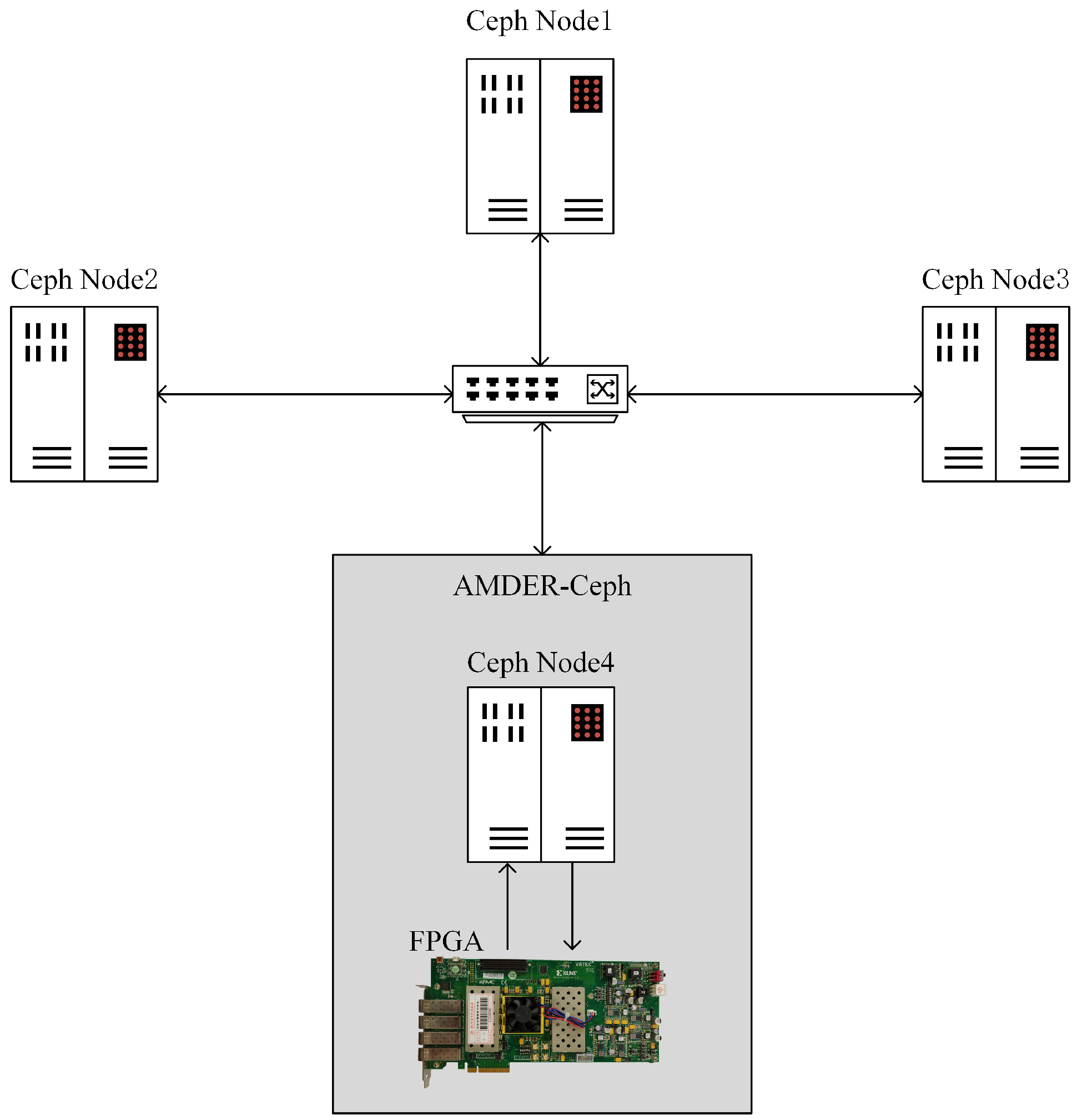
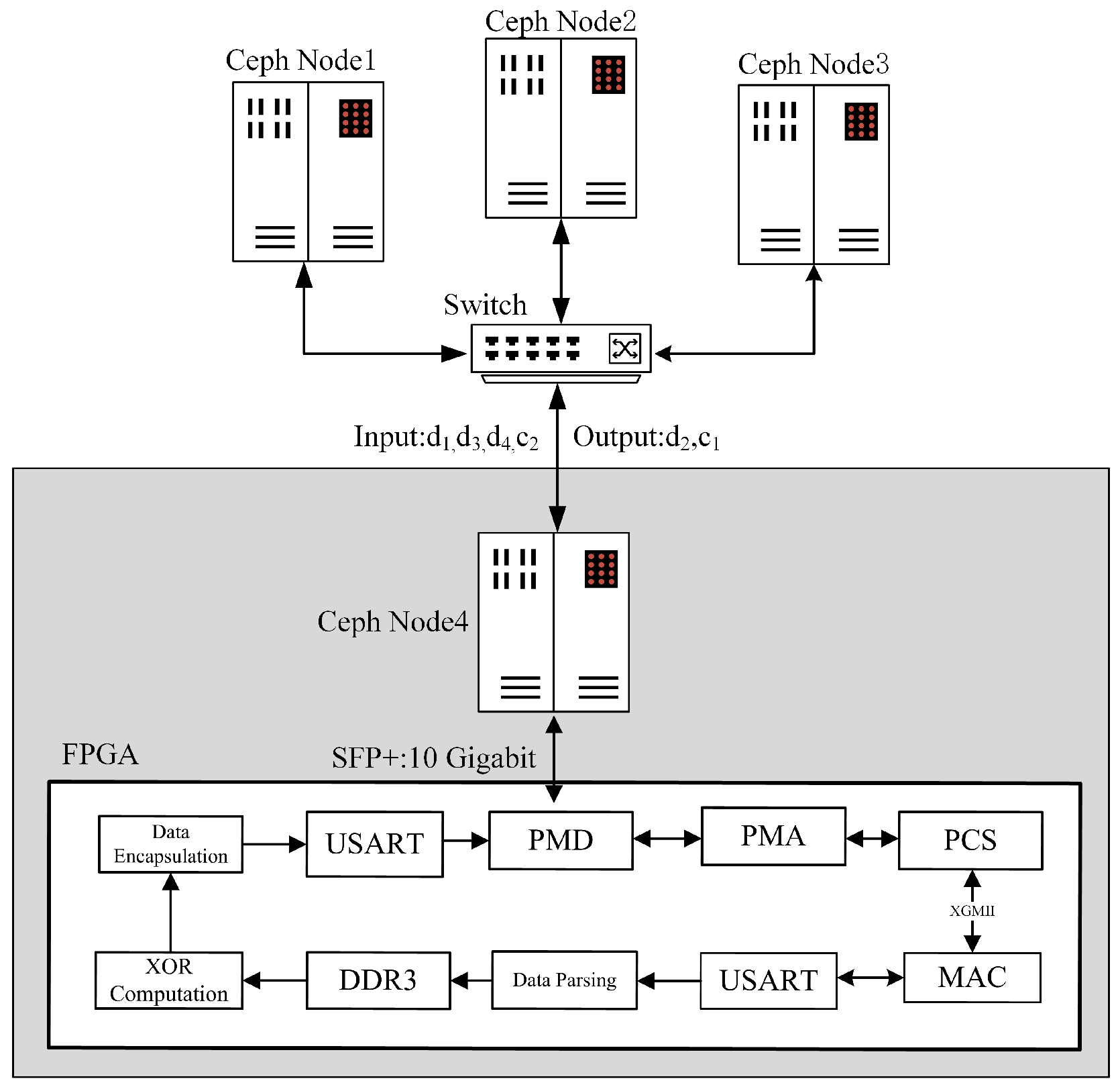
This subsection introduces the overall architectural design of the AMDER-Ceph scheme. As shown in Figure 2, the Ceph Node4 node communicates data with the FPGA through the SFP+ 10 Gigabit Ethernet interface, supporting a communication rate of up to 10 Gbps, demonstrating its powerful capabilities in high-speed data transmission. In this architecture, the clock frequencies of the various modules vary to ensure the system’s efficiency and stability. Specifically, the erasure code decoding module is driven by a 200 MHz clock, the DDR3 interface’s clock frequency is dual-edge 800 MHz, and the internal storage array operates at 200 MHz, while the other modules are controlled by a 156.25 MHz driving clock frequency.
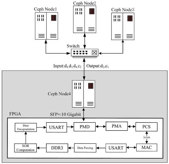
Figure 2.
Architecture of the AMDER-Ceph scheme.
In the physical layer of the AMDER-Ceph scheme, the three-layer structure, including PMD, PMA, and PCS, plays a core role. The PMD layer is responsible for physical connections, while the PMA layer performs clock recovery from the serial differential data transmitted by the PMD layer and converts it into 66-bit parallel data, and vice versa if the data come from the PCS layer. The main function of the PCS layer is to implement 64b/66b channel encoding/decoding, with data transfer to and from the MAC core being carried out through the XGMII interface. The MAC core processes lower-layer data; removes the preamble, start of frame delimiter, and frame check sequence; and converts it into MAC frames to be sent to the higher layers. For data from the higher layers, it adds the preamble and start of frame delimiter and calculates the frame check sequence.
Regarding the serial port module, the scheme merges two 64-bit data cycles from the physical layer into 128-bit data according to the AXIS bus timing during data reception. After adding the start delimiter and valid identifier, the data are sent to the decoding module. The decoding module, a core component of AMDER-Ceph, first extracts key features from the received data packets, such as source/destination MAC addresses, source/destination IP addresses, and network protocol types. For data packets that comply with ARP (Address Resolution Protocol) or ICMP (Internet Control Message Protocol), they are sent directly through the data parsing module to send automatic response packets without processing by the decoding module. For UDP (User Datagram Protocol) packets, the datagram headers are removed by the data parsing module, leaving only the data portion, which is stored in DDR3 through the DDR3 interface. The erasure code decoding module then retrieves data from DDR3 through address indexing for erasure code decoding calculations. Finally, the data encapsulation module adds datagram headers to the decoded data before sending them to the serial port module.
Figure 2 also details the entire process of data flow. After receiving the surviving Cauchy RS(4,2) data (such as , , , ) from the Ceph system, these data are first processed by Ceph Node4. At this stage, the data are converted to hexadecimal format and decoded through FPGA to recover the damaged data blocks (such as and ). Subsequently, these data blocks are distributed through Ceph’s data balancing strategy, thus ensuring the efficient and balanced operation of the entire system.
3.2. Optimization of Cauchy Matrices and Construction of Encoding/Decoding Matrices
To overcome the high consumption of computational resources by standard RS codes in the decoding process, this study leverages the natural advantages of FPGAs in performing XOR operations, drawing on the research findings of Plank et al. [41], and adopts Cauchy RS codes from the Galois field in place of traditional RS codes. Cauchy RS codes represent an innovative improvement on standard RS codes, focusing on two key aspects. First, Cauchy RS codes replace the traditional Vandermonde matrices with Cauchy matrices, significantly reducing the complexity of finding inverse matrices. This innovation not only simplifies the computational process but also effectively reduces the consumption of computational resources, especially when dealing with large-scale data. Second, another major improvement of Cauchy RS codes lies in the representation of the encoding matrix. By representing the elements of the encoding matrix in the form of binary arrays, the matrix multiplication operations in the encoding and decoding process are converted to more efficient XOR logical operations. This transformation not only improves the efficiency of encoding and decoding but also allows FPGAs to play a greater advantage in handling such operations.
3.2.1. Binary Projection Transformation
When applying RS codes for encoding and decoding in distributed storage systems, matrix multiplication operations usually require table lookups, which somewhat affects the efficiency of the computational process. For the encoding matrix in Cauchy RS codes, binary projection transformation is an effective optimization strategy [42]. This method converts the encoding matrix into a binary matrix containing only 0s and 1s, allowing the matrix multiplication operations in the encoding and decoding process to be converted to XOR operations, greatly improving computational efficiency. For any element in the finite field GF(2w), it can be represented by a binary array. In this representation, the i-th column of the binary array can be expressed in polynomial form, as shown in the following Equation (10):
where represents a column vector, the standard binary representation of the GF(2w) element. , as a bit matrix, has each column based on different powers of the element e to form a binary vector. The purpose of this representation is to convert complex GF(2w) operations into simpler, more efficient XOR operations.
Specifically, for the element e in the field GF(23) (whose values range from , with binary representations of ), its standard binary representation serves as the column vector . In addition, the element e can also be represented by a bit matrix , where the i-th column of is defined as .
For the element (binary representation 010), we first define . Then, based on the rules of operation in GF(23) (i.e., all calculations are performed modulo 8), we calculate each column of : and . The results show that the first column of corresponds to , the second column corresponds to , and the third column corresponds to . In GF(23), these calculations only consider the last three binary digits of the result. Hence, we derive the following Equation (11):
Using Algorithm 1, the elements of the finite field GF(23) are represented by the binary array , and the encoding matrix is transformed into an binary encoding matrix. In traditional RS codes, the parameter w needs to be larger than the data bit width, which often results in the selection of the finite field being restricted to larger scales, such as GF(28), GF(216), or GF(232). However, Cauchy RS codes offer greater flexibility in this respect. In the design of Cauchy RS codes, the selection of w only needs to satisfy the condition that , where k is the number of data blocks, and m is the number of parity blocks. This means that, compared with RS codes, Cauchy RS codes allow the use of smaller finite fields to perform encoding and decoding operations. This characteristic not only reduces computational complexity but also decreases the demand for storage space while improving the efficiency of encoding and decoding.
| Algorithm 1 Calculation of matrix for element e in GF(23) |
|
3.2.2. Construction of Encoding/Decoding Matrices
Following the principles of the binary matrix construction algorithm, we construct the encoding matrix for Cauchy RS(8,4) on the finite field GF(24). Initially, four elements, , are selected from the field to form the set A, and then eight elements, , are chosen to form the set B. Based on these two sets and Equation (10), a Cauchy matrix is generated. Subsequently, binary conversion is performed according to Equation (10), a process that demands relatively low storage resources; the RAM storage space required for the converted matrix is only bits = 64 bytes.
As shown in Equation (12), the encoding matrix M contains four different Cauchy RS codes (Cauchy RS(8,1), Cauchy RS(8,2), Cauchy RS(8,3), and Cauchy RS(8,4)) encoding matrices. In practice, depending on the required error correction capability, one can flexibly choose the number of rows in the encoding matrix. For example, when m is less than 4, taking the first rows from the matrix constitutes the encoding matrix for Cauchy RS(8,m).
The decoding process follows a similar principle. Depending on the type of data block to be recovered (whether data or parity block), the corresponding rows are selected from the complete binary encoding matrix to construct the corresponding decoding matrix. This flexible row selection mechanism ensures that, even in the face of lost or damaged data blocks, data recovery operations can be effectively executed.
3.3. Implementation of Parallel Parity Generators and Decoders
3.3.1. Parallel Parity Generator
In the AMDER-Ceph decoding design for distributed storage systems, the parallel parity generator plays a key role in generating parity messages. As shown in Table 3, the AMDER-Ceph scheme has designed a parallel parity generator responsible for executing XOR operations on a pair of adjacent data messages and . During the operation, only columns to and to of the binary encoding matrix are used. This strategy aligns with the usage principles of the binary arrayed Cauchy encoding matrix in the AMDER-Ceph scheme, aiming to improve the efficiency of the data recovery process.
Table 3.
Interface specification of the parallel parity generator.
In the AMDER-Ceph scheme, the output of the parallel parity generator is not the final parity message but serves as an intermediate variable for further calculations. After all modules complete their calculations, these intermediate variables will be aggregated and XORed to generate the final parity message. This step is hardware-accelerated at the FPGA level, in line with the goals of the AMDER-Ceph scheme, namely, to improve the processing speed of erasure codes through hardware acceleration.
The signal interfaces of the module reflect the AMDER-Ceph scheme’s pursuit of efficient data transmission and processing. clk (clock signal) and reset (reset signal) ensure the module’s synchronization and reset capability. input_valid, input_ready, and output_valid form a handshake protocol, ensuring the correctness of data transmission between modules and preventing errors in high-speed data processing. At the same time, the busy signal provides status feedback, an important part of flow control between modules.
The input signals and are 256 bits wide, representing adjacent data messages and , each 64 bits representing a data group within the message. This design allows the module to process data in parallel, reducing the potential bottlenecks caused by serial processing.
The input of the encoding matrix is through signals to , each 8 bits wide. These signals’ bit segments [7:4] and [3:0] correspond to consecutive columns of the encoding matrix, allowing the module to perform calculations according to the binary encoding matrix specified in the AMDER-Ceph scheme. The output signals , , , and carry the calculated intermediate variables, which will eventually be combined into a complete parity message. Through this design, the AMDER-Ceph scheme achieves efficient data recovery processes at the FPGA level, especially when handling large-scale data blocks, providing a significant performance enhancement.
3.3.2. Decoder
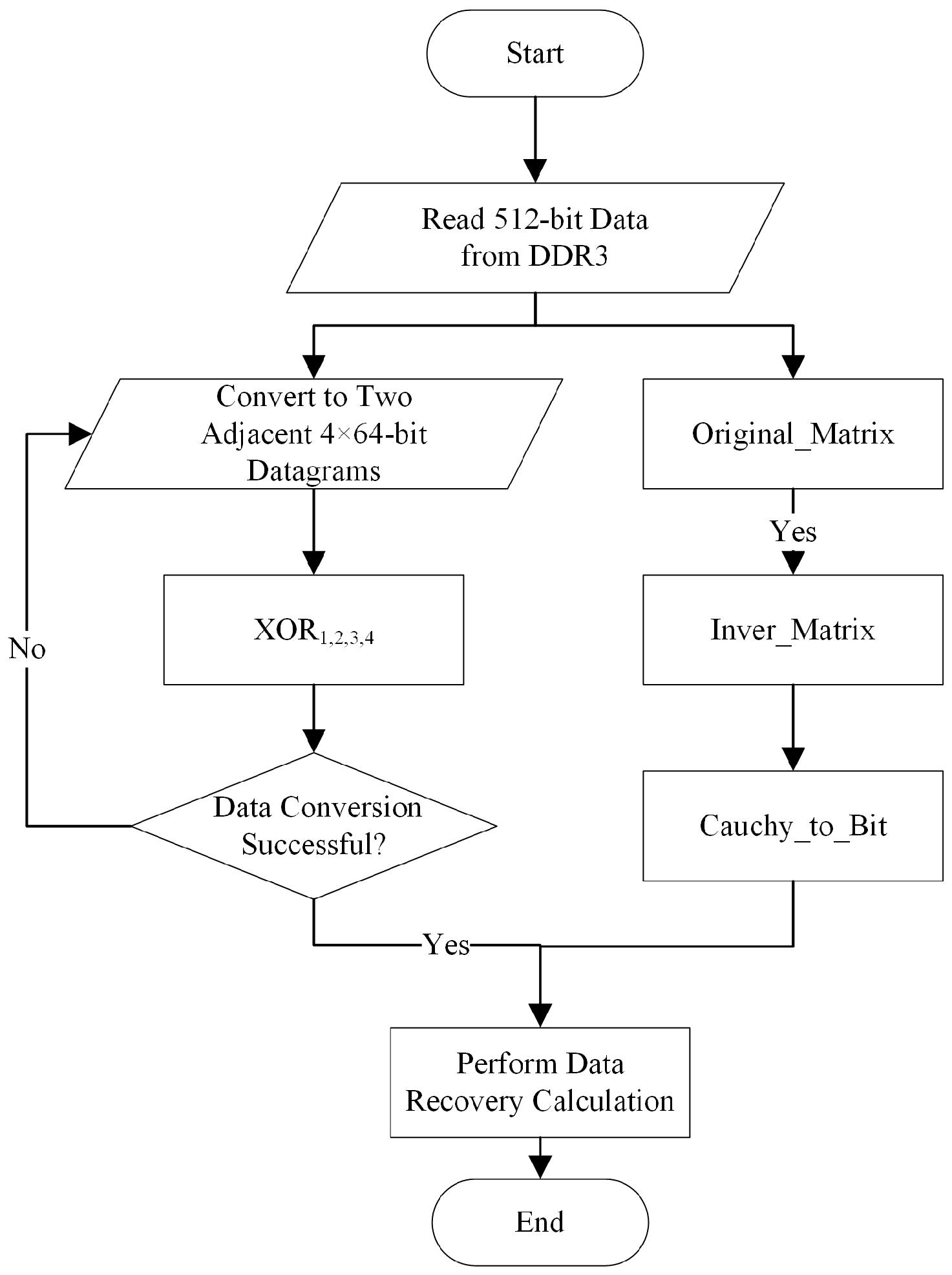
In the encoding and decoding processes of Cauchy RS codes, the core steps are inseparable from matrix operations on the finite field GF(2w). The main difference between the two is that the decoding stage requires the calculation of the inverse matrix. The AMDER-Ceph scheme cleverly utilizes the parallel computing capabilities of FPGAs to significantly reduce the computational complexity required to find the inverse matrix, thus effectively improving the efficiency of data recovery. Figure 3 illustrates the workflow of Cauchy RS code decoding, ensuring that even in the face of data corruption or loss, the original data can be quickly and accurately recovered.
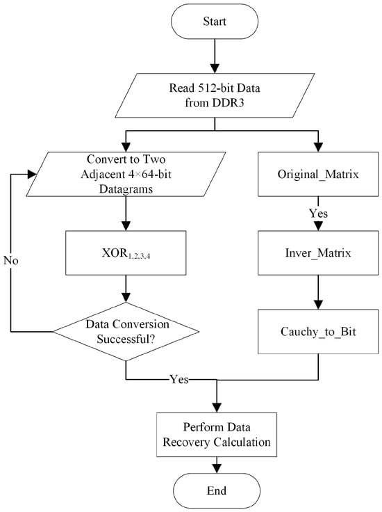
Figure 3.
Workflow of Cauchy RS code decoding.
In the decoding workflow of the AMDER-Ceph scheme’s Cauchy RS codes, hardware acceleration is used to enhance the recovery efficiency of four Cauchy RS codes: Cauchy RS(8,1), Cauchy RS(8,2), Cauchy RS(8,3), and Cauchy RS(8,4). The algorithm is defined over GF(24) with the primitive polynomial . Data messages are divided into four 64-bit data groups, with a total size of 256 bits. The decoding module includes four specially designed XOR logic units (XOR1, XOR2, XOR3, XOR4), responsible for performing decoding calculations. The 512-bit wide data read from DDR3 is converted into two adjacent 4 × 64-bit data messages, and , by the preprocessing module. At the same time, the original matrix Original_Matrix, upon inversion to Inver_Matrix, is then binary-arrayed to form Cauchy_to_Bit and Decode_Matrix. Once the data conversion is complete, multiplying the matrix Decode_Matrix with the surviving data yields the lost data.
Specifically, in the Cauchy RS encoding process, each data packet is divided into w data groups, with the size of the data packet representable as , where the bit width of the data group, packetsize, is generally a multiple of 8 bits. Taking Cauchy RS(4,2) as an example, when the parameter for the finite field, its encoding process is illustrated in Figure 4. When and are damaged, the decoding recovery process is shown in Figure 5.
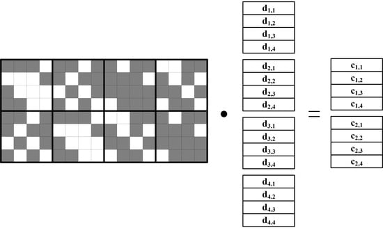
Figure 4.
Cauchy RS(4,2) encoding process over GF(24).

Figure 5.
Decoding recovery process when and are corrupted.
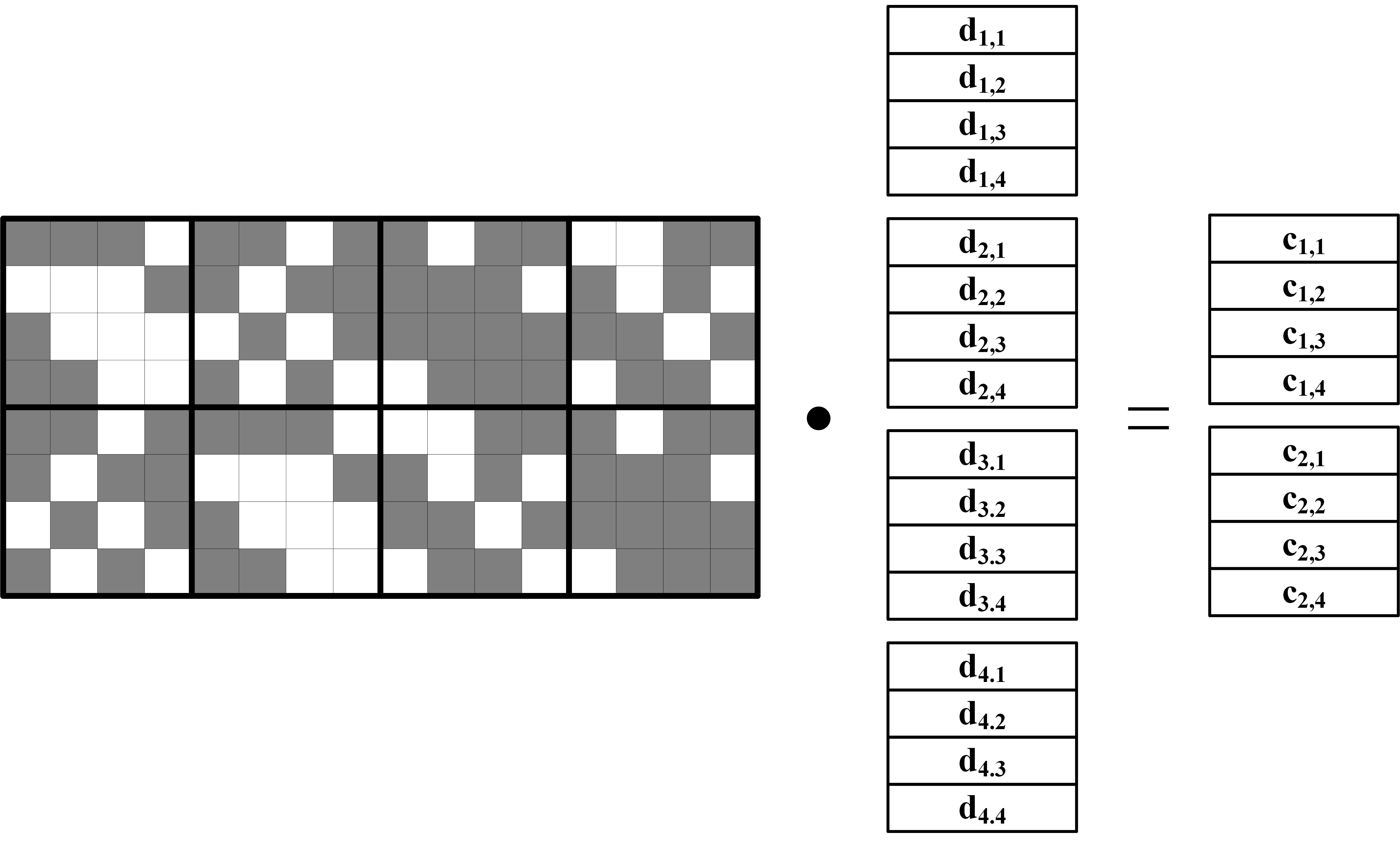
In the diagrams, , , , and respectively represent the first, second, third, and fourth data groups of the first data message. The others follow similarly. Since only 0s and 1s exist in the binary encoding matrix, the encoding calculation process only needs to perform XOR logical operations to obtain the parity messages. For example, taking the first data group of the parity message as an example, the calculation is implemented according to the fifth row of the binary encoding matrix, as shown in the following Equation (13):
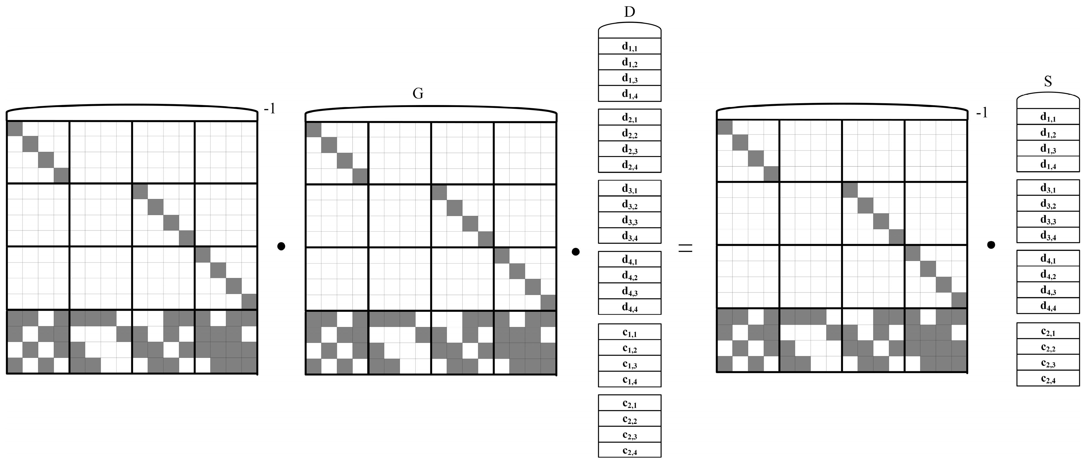
When and are corrupted, four elements are selected from the still valid codewords to form the column vector , and rows at the same positions as the codewords in the column vector S are used from the generator matrix to form a matrix G. If the surviving data elements’ column vector is denoted by D, then it is clear that holds. At this point, multiplying both sides of this equation by the inverse of the matrix G, the data elements can be recovered, and the invertibility of the matrix G has been proven by Equation (13), which is not discussed further here.
3.4. Latency Analysis and Optimization
3.4.1. Latency Analysis
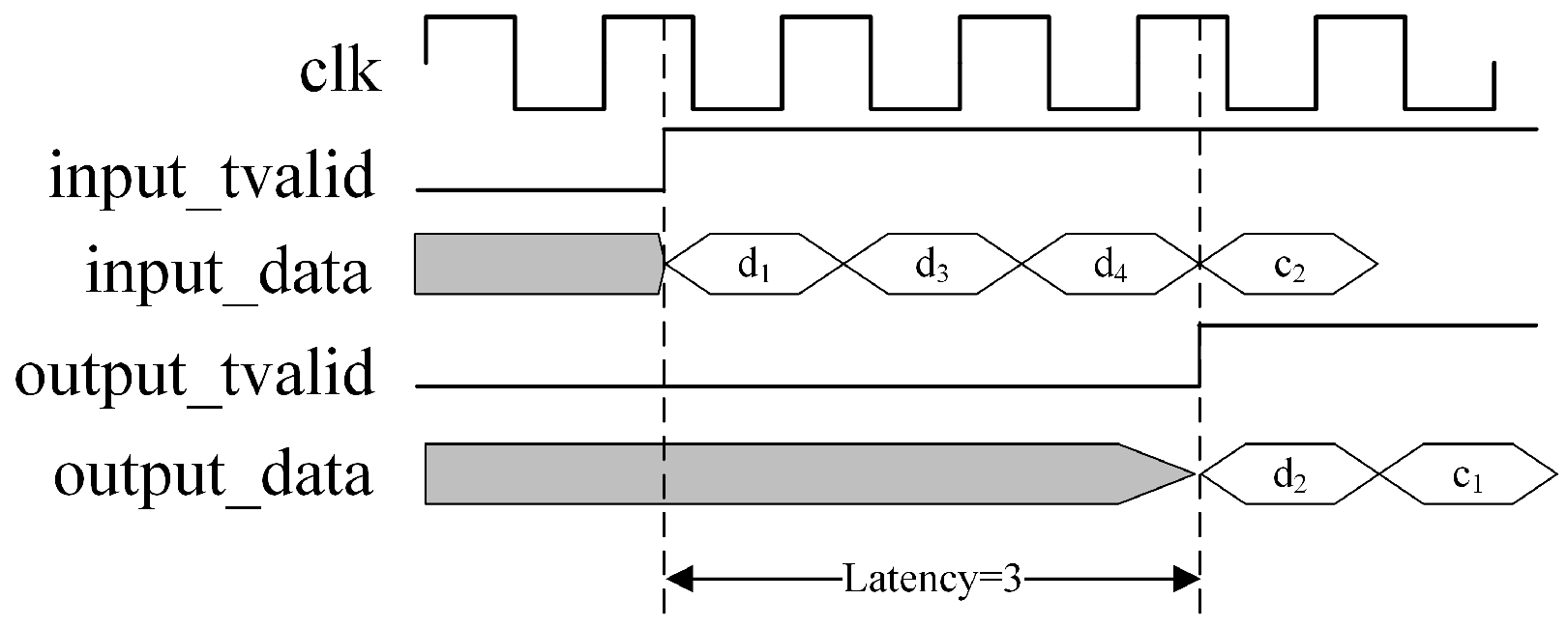
In the official Xilinx documentation for the Reed–Solomon Decoder v9.0 LogiCORE IP, latency is defined as the number of clock edges from when a symbol is sampled on DATA_IN until the corrected version of that symbol appears on DATA_OUT. An example with a latency of three clock cycles is shown in Figure 6, although actual latency is often much greater than this value.
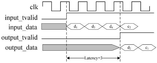
Figure 6.
Illustration of latency in the Reed–Solomon decoder.
Latency depends on several factors, including the number of data blocks k, the number of parity blocks m, symbol width, the number of channels, etc. If the processing latency exceeds the block length, the latency may vary. The FPGA core can buffer data for the next block while still processing the previous block. In such cases, it must wait until the previous block is processed, which adds to the new block’s latency.
Equation (14) is used to estimate the latency of a Reed–Solomon decoder without erasure decoding. The calculation relies on half the number of correctable errors t, the number of symbols in a codeword n, and the number of channels used (num_channels). In general, L provides a quantitative measure of the performance of the Reed–Solomon decoder under specific configurations.
Latency is a more comprehensive concept that encompasses the total time taken by the Reed–Solomon decoder from receiving data to outputting the corrected data. It includes not only the L value calculated using Equation (14) but may also include other factors such as internal processing time and storage read buffer delays. Overall, latency is a broader measure of the performance of a Reed–Solomon decoder, including the combined impact of multiple factors, as shown in the following Equation (15):
Here, m (Symbol Width = 8) takes a value of 1 when the symbol width equals 8 bits, and 0 otherwise. (Number Channels > 1) takes a value of 1 when the number of channels is more than one, and 0 if the number of channels is less than or equal to one. Furthermore, in the AMDER-Ceph scheme, frequent data reads from DDR3 are a key step, but the read operation is accompanied by a Column Address Strobe latency [43] (), an inherent delay that reduces data processing efficiency. CAS latency refers to the waiting time for data to be transmitted to the FPGA data bus and prepared for output after the control and address signals are triggered. As shown in Figure 6, in the AMDER-Ceph scheme, a latency of 50–60 clock cycles may exist from the initiation of a read data request to data recovery, which significantly impacts the efficiency of data recovery.
3.4.2. Latency Optimization
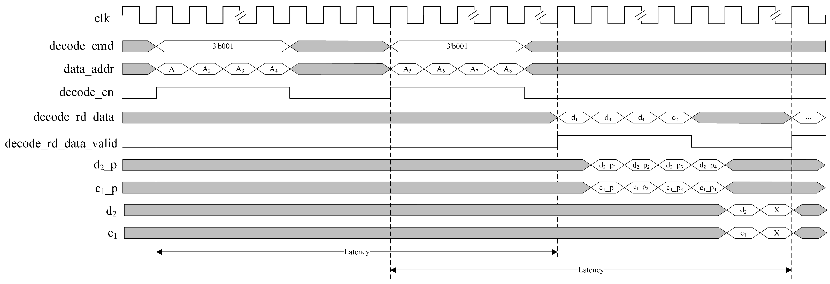
In the data recovery process on FPGAs, ensuring precise timing between modules is crucial for the reliability and efficiency of data transfer. Batch reading large amounts of data for decoding to increase efficiency may increase the difficulty of inversion operations, causing latency in FPGA logic units and failing to meet timing requirements, affecting overall performance and resource optimization. To address this issue, this paper proposes a timing optimization strategy. This structure aims to implement Cauchy RS encoding data recovery in FPGA, optimize timing requirements, and reduce the complexity of inversion operations. The timing strategy for data recovery when and data are corrupted is shown in Figure 7. This figure builds upon our team’s previous work [39], ensuring performance while maximizing the frequency and efficiency of the FPGA design.
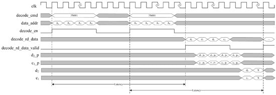
Figure 7.
Timing diagram of data recovery with tiered parallel processing structure.
Figure 7 describes the proposed timing optimization strategy in the case of losing two nodes and performing full node recovery in Cauchy RS(4,2). The strategy allows each parallel decoding operation to handle two message stripes. Each decode_rd_data read from DDR3 contains two adjacent 32-byte data block slices, and . Therefore, a complete decoding cycle under this optimization strategy can process two original 256-byte data, totaling 512 bytes, eventually generating two message stripes. Figure 7 also shows the AMDER-Ceph scheme completing the read address request for message stripes and decoding calculations for lost data in the first message stripe within two latency intervals. Quantitative analysis indicates that the decoding time consumption of this timing optimization strategy is approximately one latency plus the computational delays for two sets of decoded data, effectively reducing the impact of latency on decoding efficiency.
First, in the example in Figure 7, the AMDER-Ceph scheme optimizes the read timing of DDR3. After issuing read commands and address requests for the first set of data, a wait time is allowed, sufficient for all intermediate variable calculations and check data message calculations of the first set of data, and then read commands and address requests for the second set of data are issued. This timing optimization ensures that both data requests are completed within the latency of the first set of data, allowing decoding operations for the first set of data within the latency of the second set.
Second, this paper deeply optimizes the XOR operation process of the Cauchy RS code, breaking down the decoding calculation process and decomposing large combinational logic into smaller logic units. After calculating the intermediate variables through the XOR logic module, these variables are used to compute the decoded data, ensuring the reliability of data transmission between modules. In the AMDER-Ceph scheme, the data read from DDR3 includes the data message of a message stripe, and each storage block at the address contains two adjacent data messages. When arrives at the next clock cycle, calculations for the first set of intermediate variables, and , in the first message stripe are performed. After completing this calculation, a similar processing for the second set of intermediate variables continues, thus completing the entire decoding cycle and processing a total of 512 bytes of data. The calculation process for the first set of intermediate variables, and , for the decoded recovery data and in the first message stripe can be expressed by the following Equation (16):
where the decoding matrix is extracted from the original encoding matrix and the identity matrix I, with and representing the first and second column vectors of the matrix . When the signal outputs, it indicates that the first set of data has been read completely. Subsequently, the system completes all intermediate variable calculations for the first message stripe within one clock cycle. When the next clock rising edge arrives, the system begins to compute the decoded data message and parallelly outputs the results. In Figure 7, and represent the decoding results for the first message stripe, and X can represent the calculated results for the second message stripe. Taking as an example, the calculation process for its check message follows the following Equation (17):
3.5. Resilience Strategies for Multi-Dimensional Recovery in Multiple Block Failure Scenarios
In the simulation of the AMDER-Ceph scheme for data recovery, this study employed a unique strategy: randomly inducing the failure of the maximum number of data or parity blocks within the Ceph distributed storage system. This method aims to assess the recovery capabilities of the AMDER-Ceph method in handling extreme and uncertain data corruption scenarios. For instance, under the Cauchy Reed–Solomon (8,4) coding configuration, we randomly selected up to four data or parity blocks for failure induction in the Ceph system testing pool, thereby simulating possible worst-case data corruption scenarios.
This simulation strategy particularly underscores the role and significance of the Ceph distributed storage system. Both upload and related download algorithms must adapt to random block failures occurring within the Ceph system. The upload script must handle efficient uploading in scenarios of partial data loss, whereas the download script needs to facilitate recovery from various patterns of data corruption in the Ceph storage pool.
In the implementation of Algorithm 2, the name of the target Ceph storage pool is first defined (POOL_NAME="my-pool"), and a list of files (FILES), containing all filenames intended for upload, is created. A loop structure iterates over the file list, conducting existence checks for each file. If a file exists, its object name is extracted from the filename, and the rados command is executed for file upload. During the upload process, the algorithm verifies the upload status of each file. If an upload fails, an error message is outputted and the operation is terminated; if all files are successfully uploaded, a confirmation message is outputted. This algorithm ensures data safety and integrity within the Ceph storage pool.
| Algorithm 2 Algorithm for uploading files to the Ceph storage pool |
|
In the AMDER-Ceph scheme, a parallel file downloading algorithm, Algorithm 3, was also designed and implemented for efficient file downloading from the Ceph cluster. This algorithm employs Python’s concurrent.futures module and a thread pool to achieve parallel downloads, significantly enhancing the efficiency of the data recovery process. The input is a dictionary containing filenames and paths, and the output is the download status for each file.
In the context of random block failures, the parallel download capability of the download script becomes particularly crucial. It not only improves the efficiency of downloading data from the Ceph storage system but also quickly addresses and recovers data gaps caused by random data corruption. The implementation process first defines the name of the Ceph storage pool (pool_name=’my-pool’) and then uses the download_file_from_ceph function with the subprocess module to execute the rados command for downloading specified files from the Ceph cluster. If the download is successful, the function returns a confirmation message; if an error occurs, it returns an error message. The main functionality is achieved through the download_files function, which initializes a thread pool with four workers and submits download tasks for processing. The algorithm records the start and end times of the download operations, calculates, and outputs the total download duration, thus providing data to evaluate download efficiency.
These simulations within the Ceph distributed storage system not only validate the theoretical error-correction capabilities of the AMDER-Ceph method but, more importantly, demonstrate its strong adaptability and recovery abilities in the face of unpredictable real-world data corruption scenarios.
| Algorithm 3 Algorithm for parallel file downloading from the Ceph cluster |
|
4. Performance Evaluation of AMDER-Ceph
This section presents a detailed performance evaluation of the AMDER-Ceph system. To ensure fairness and accuracy in our assessment, we selected files of various sizes for testing, including 10 KB, 100 KB, 1 MB, and 4 MB. Additionally, we evaluated different erasure coding configurations, such as Cauchy Reed–Solomon (RS) codes of (8,2), (8,3), and (8,4). For a comparison with existing technologies, we chose native Ceph-supported erasure coding data recovery plugins: Jerasure, Clay, ISA, and Shec, as control groups.
The objective of this section is to assess the acceleration effect of AMDER-Ceph on different fault tolerance levels of Cauchy RS codes with varying data volumes. Our primary focus is on throughput, a core performance metric, which can be calculated using the following Equation (18):
where k represents the number of surviving data blocks, n the size of each data block, and the total time from data transmission to successful recovery. is the throughput, measured in MB/s.
4.1. Experimental Setup and Methodology
Before describing the experimental environment, let us first introduce the experimental topology structure and the decoding recovery process of the AMDER-Ceph scheme.
The experiment was conducted in a Ceph cluster consisting of four machines, one of which was equipped with AMDER-Ceph, namely, a host machine plus an FPGA. These machines were interconnected through an H3C-S6520 switch, forming a complete Ceph storage cluster. The AMDER-Ceph host is responsible for managing the FPGA and communication with other Ceph nodes. Figure 8 illustrates the experimental topology.
The AMDER-Ceph scheme details a FPGA-based data processing and decoding workflow, as shown in Figure 9. The process is divided into the following steps:
Step 1: Data Reception and Preprocessing. Upon initialization, AMDER-Ceph receives packets from the Ceph storage system, containing surviving data and necessary protocol information. Next, the FPGA extracts packets via its SFP+ interface and parses them internally to separate protocol headers from data payloads.
Step 2: Data Caching and Matrix Preparation. The FPGA caches the parsed packet headers for subsequent forwarding. Concurrently, it checks if the memory (DDR3) is ready to receive data. If ready, data payloads are written into DDR3; otherwise, it waits until the memory becomes available.
Figure 8.
Experimental topology.
Figure 8.
Experimental topology.
Step 3: Inverse Matrix Calculation and Decoding Preparation. While caching data payloads, the FPGA also calculates the coefficient matrix CM of the failed encoding blocks and further computes its inverse, CM−1. Once the computation is complete and all data are received and cached, decoding begins; otherwise, it waits for full data caching.
Step 4: Data Decoding and Recovery. After completing the CM−1 matrix computation, the FPGA reads data from memory and performs decoding, involving multiplication with the coefficient matrix DPk, and subsequent recovery operations for the failed data blocks. Upon completing decoding for all data stripes, data are sent; if not, the process returns to the previous step for continued decoding.
Step 5: Data Packaging and Forwarding. Finally, based on pre-cached protocol header information, the recovered data are encapsulated and sent back to the Ceph storage system through the network. This process repeats until all data stripes are processed, completing the decoding workflow.
Throughout the process, Num_stripes denotes the number of message stripes requiring decoding, while variables like CM and DPk have been defined in Section 2. In our proposed scheme, the computation of a fourth-order matrix inverse requires only 11 clock cycles, and constructing the coefficient matrix CM and performing binary array conversions each require one clock cycle. Conducted at a 200 MHz frequency, the total computation time is 65 nanoseconds. Given the high-speed Ethernet transmission rate of 10 Gbit/s, theoretical analysis indicates that when the transmitted data volume exceeds 81.25 bytes, matrix computation does not become a bottleneck for data reception and caching in DDR3. Specifically, for the Cauchy RS code decoding process implemented in the AMDER-Ceph scheme, given the fixed size of 32 bytes per encoded message, the time overhead for matrix inversion is negligible, thus effectively optimizing the timing of data processing and ensuring that matrix operations do not become a limiting factor during high-speed data transmission.
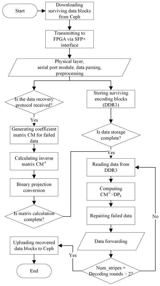
Figure 9.
AMDER−Ceph scheme decoding workflow.
Figure 9.
AMDER−Ceph scheme decoding workflow.

4.1.1. Experimental Hardware and Software Environment
The hardware platform used in the experiments was the Xilinx VC709 FPGA development board [33]. The Xilinx VC709 board offers high parallelism, flexibility, low latency, high-bandwidth interfaces, and powerful development tools, facilitating the development of efficient, customizable, and low-power data recovery solutions. Table 4, Table 5 and Table 6 present the main parameters of the hardware environment used in our experiments, while Table 7 details the main parameters of the software environment, and Table 8 outlines the main parameters for decoding performance tests.
Table 4.
FPGA development board experimental hardware environment.
Table 5.
Ordinary Ceph node experimental hardware environment.
Table 6.
AMDER-Ceph host experimental hardware environment.
Table 7.
Experimental software environment.
Table 8.
Decoding performance test main parameters.
4.1.2. Experimental Methodology
The experiments were divided into two parts: testing with native Ceph plugins and testing with AMDER-Ceph.
Testing with Native Ceph Plugins: For the performance testing of the Ceph storage system, especially using the Jerasure, Clay, ISA, and Shec decoding plugins, we developed a series of Bash scripts to evaluate throughput with different data volumes and erasure coding configurations. These scripts were designed to test a range of file sizes, specifically 10 KB, 100 KB, 1 MB, and 4 MB, and to explore multiple erasure coding configurations, including Cauchy RS(8,2), RS(8,3), and RS(8,4). The initial steps of the experiment involved creating a file named results.csv to collect and store all test data. Then, using the ceph osd erasure-code-profile set and ceph osd pool create commands, we meticulously configured the required erasure coding parameters and established the corresponding storage pools. Through the rados bench command, we conducted benchmark tests for different file sizes and erasure coding configurations. To obtain reliable data, each configuration combination was tested 1000 times to calculate the average throughput. Upon completing data recovery and verifying data consistency, all test data were precisely recorded in the results.csv file, providing a rich data resource for subsequent analysis. Figure 10 shows the specific flowchart of the Ceph decoding plugin test script.
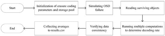
Figure 10.
Ceph plugin test script flowchart.
Testing with AMDER-Ceph: To thoroughly evaluate the performance of AMDER-Ceph in practical applications, we formulated a comprehensive test plan focused on measuring its interaction efficiency with the Ceph cluster and its decoding performance. Initially, it was essential to ensure that AMDER-Ceph could smoothly connect and interact with the Ceph cluster. Subsequently, we used the same file sizes as in the tests with the native Ceph plugins—including files of 10 KB, 100 KB, 1 MB, and 4 MB—and the same erasure coding configurations, such as Cauchy RS(8,2), RS(8,3), and RS(8,4). Throughput was the core metric for assessing the performance of AMDER-Ceph. For this purpose, we meticulously analyzed the time taken to download files from the Ceph cluster to AMDER-Ceph (), the time to transfer files from the host to the FPGA platform (), the file decoding time on the FPGA platform (), and the time to upload files from AMDER-Ceph back to the Ceph cluster (), considering the sum of these time periods as the total processing time ().
By comparing the throughput of AMDER-Ceph with that of the native Ceph plugins, we could precisely evaluate its performance and efficiency. Additionally, by analyzing the time consumption at each stage, we were able to identify potential performance bottlenecks and suggest directions for improvement. This series of tests not only comprehensively examined the performance of AMDER-Ceph but also provided a solid data foundation for its future research development and practical deployment.
4.2. Experimental Results and Analysis
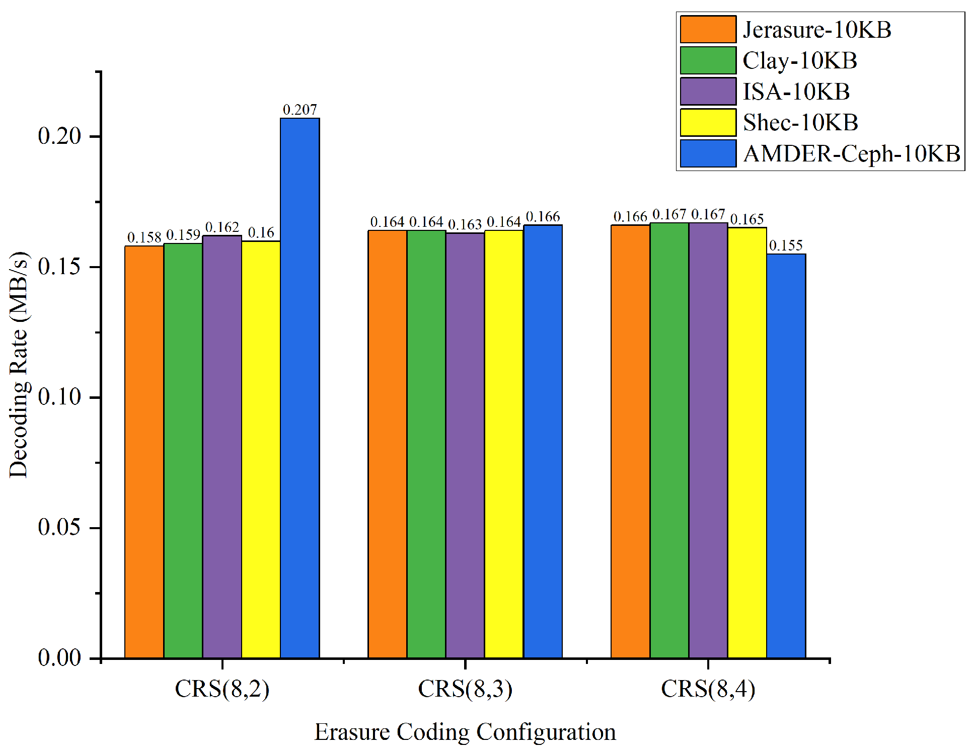
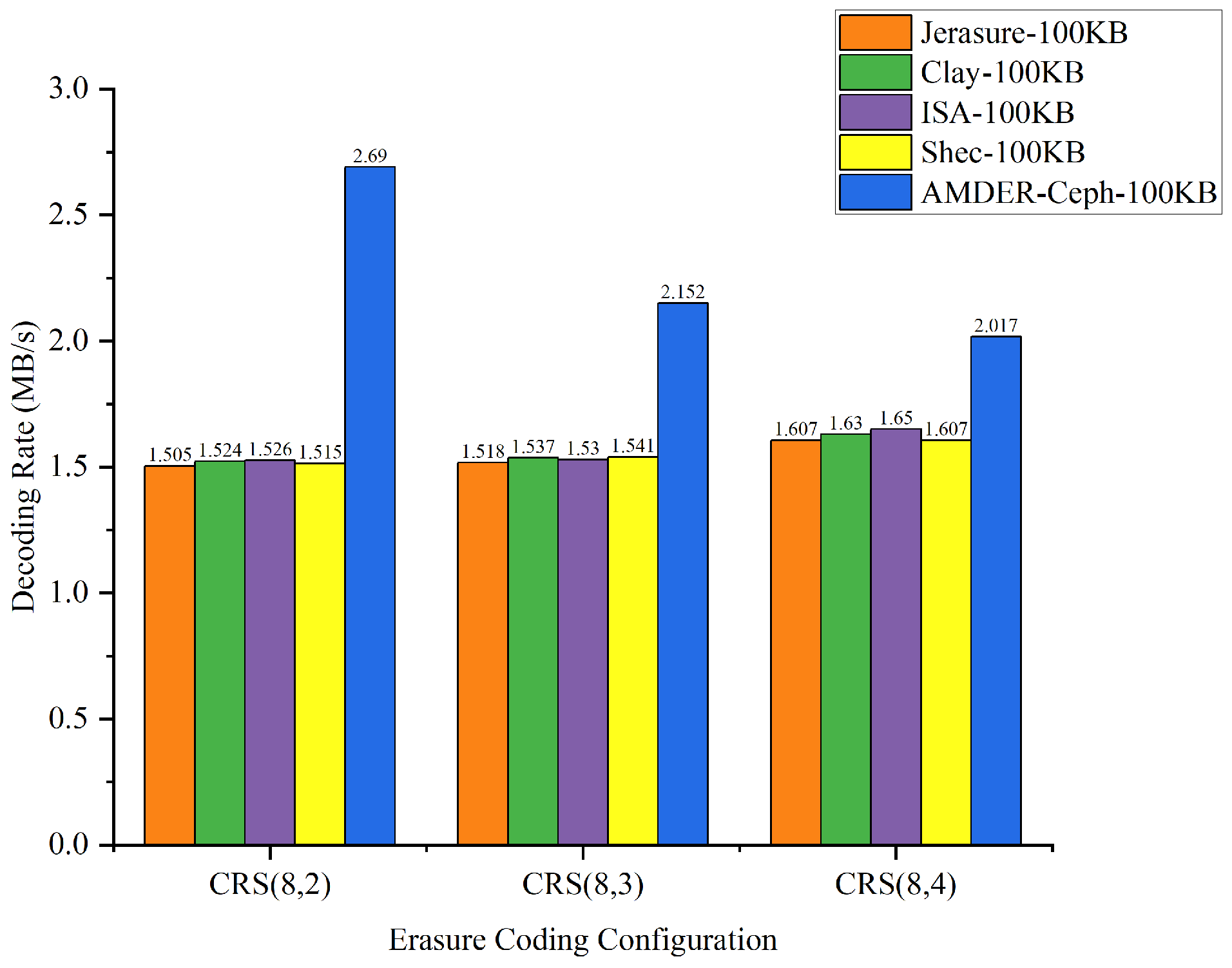
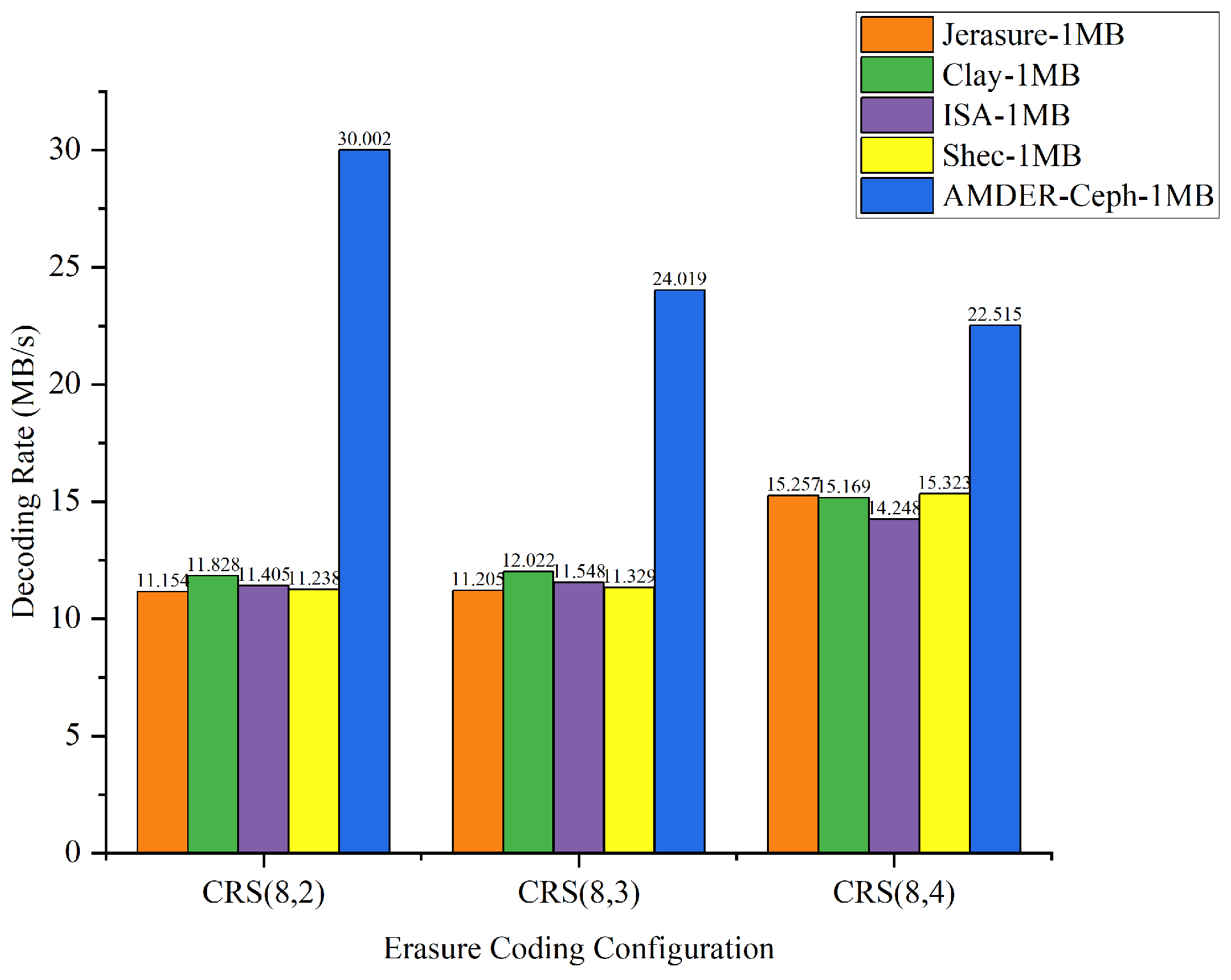
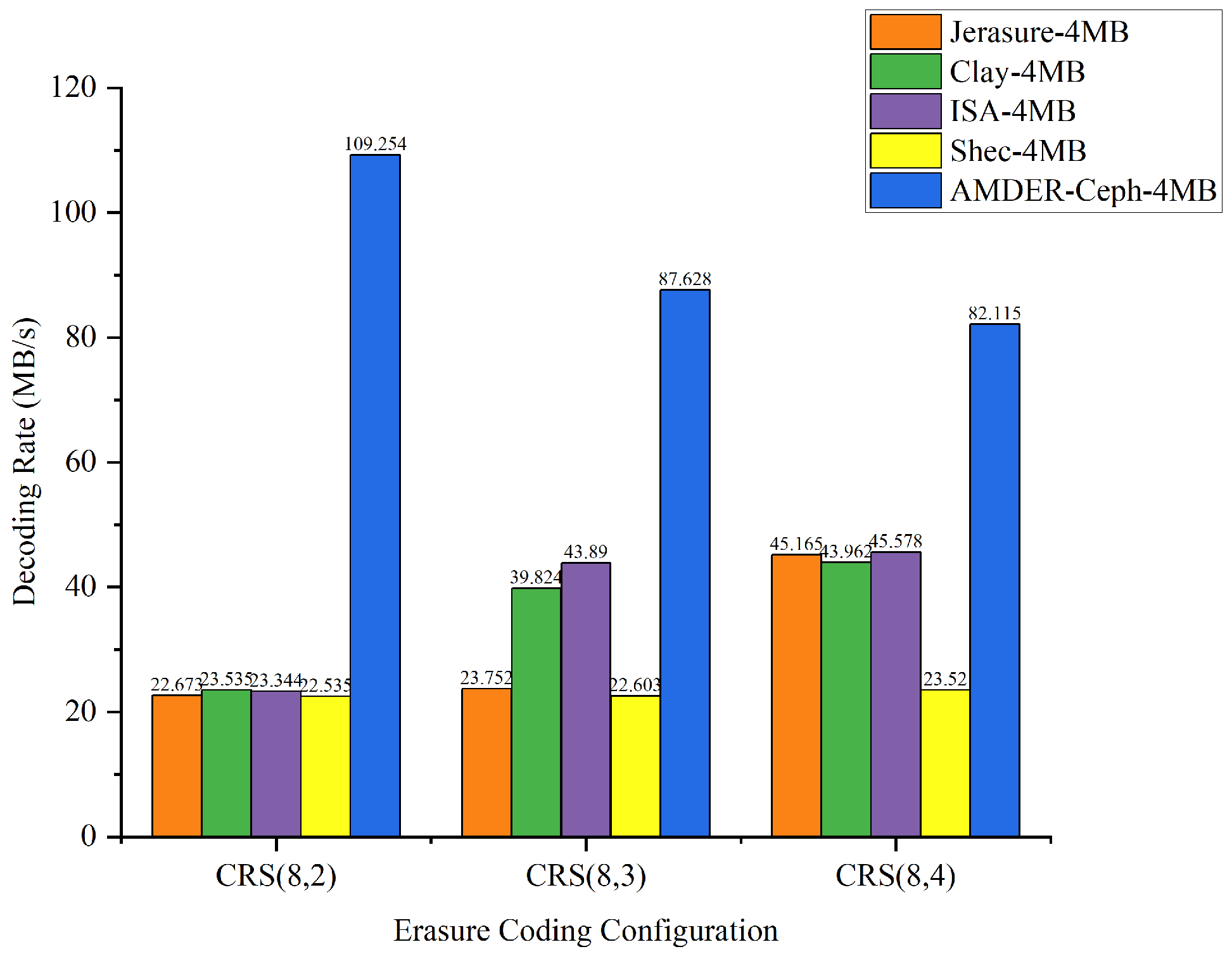
The goal of this experiment was to delve into how erasure coding configurations, file sizes, and plugins collectively influence throughput. Through a series of comprehensive tests, we obtained a set of detailed data, presented in Table 9. To further explore how these factors interact and affect throughput, we converted Table 9 into Figure 11, Figure 12, Figure 13 and Figure 14, illustrating the data throughput for different erasure coding configurations at file sizes of 10 KB, 100 KB, 1 MB, and 4 MB, respectively.
Table 9.
Throughput under different erasure coding configurations and file sizes.

Figure 11.
Data throughput for different erasure coding configurations with 10 KB file size.

Figure 12.
Data throughput for different erasure coding configurations with 100 KB file size.
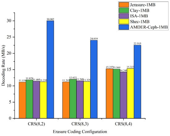
Figure 13.
Data throughput for different erasure coding configurations with 1 MB file size.

Figure 14.
Data throughput for different erasure coding configurations with 4 MB file size.
From the perspective of file sizes, AMDER-Ceph exhibited excellent performance across various file dimensions. For smaller 10 KB files, although the inherent startup latency and data transmission overhead of the FPGA might result in a slightly lower throughput for AMDER-Ceph compared with native Ceph plugins, its performance advantage becomes significant as file size increases to 100 KB, 1 MB, and especially 4 MB. This indicates that, with increasing file size, AMDER-Ceph effectively overcomes the initial latency, leveraging the powerful parallel processing capabilities of the FPGA. In the tests with 4 MB files, AMDER-Ceph, utilizing its optimized data flow processing and the FPGA’s parallel computation capabilities, achieved a throughput of 109.254 MB/s under the Cauchy RS(8,2) configuration, significantly surpassing other plugins.
Furthermore, from the perspective of erasure coding configurations, AMDER-Ceph outperformed traditional Ceph plugins such as Jerasure and ISA in all tested configurations, including Cauchy RS(8,2), RS(8,3), and RS(8,4). This performance difference is attributed to AMDER-Ceph’s hardware-specific optimizations on the FPGA, including dedicated hardware acceleration and low-latency optimization, as well as more efficient memory bandwidth utilization. Additionally, the AMDER-Ceph scheme’s software stack is more streamlined, reducing additional protocol and operating system overheads, allowing it to process large files more quickly.
In summary, AMDER-Ceph demonstrated a clear performance advantage in decoding tasks for medium to large files. Particularly with the Ceph system’s default block size of 4 MB, its performance enhancement was most pronounced, reaching up to 4.84 times. This significant performance improvement highlights the FPGA’s powerful potential in handling intensive, large-scale data workloads and AMDER-Ceph’s advanced design in hardware acceleration and algorithm optimization. These findings not only provide valuable data support for enhancing and optimizing the performance of Ceph storage systems but also point out further directions for development in hardware and software co-design.
5. Conclusions and Future Outlook
The significance of this study lies in its potential to substantially improve data recovery processes in distributed storage systems, particularly in handling multiple block failures. By integrating FPGA hardware acceleration with advanced erasure coding techniques, this research offers a viable solution for enhancing the robustness and efficiency of Ceph-based storage infrastructures. The implications of these findings extend beyond Ceph systems, suggesting potential applications in other distributed storage environments where data integrity and recovery speed are critical.
This paper has delved into an FPGA-based multi-dimensional elastic recovery acceleration method in multiple block failures within the Ceph system. By proposing the AMDER-Ceph scheme, this study combined multi-dimensional elastic recovery strategies with FPGA hardware acceleration, enhancing the efficiency and performance of the Ceph storage system during data recovery. The AMDER-Ceph scheme, through optimizing encoding and decoding matrices and implementing efficient decoders, fully leveraged the FPGA’s parallel computing capability, significantly boosting the throughput of erasure code decoding. Experimental results showed that AMDER-Ceph exhibited significant performance improvements over native Ceph erasure code libraries in various erasure coding configurations and file sizes, especially with Ceph’s default data block size of 4 MB, where performance was notably enhanced, reaching up to 4.84 times.
Exploration of future development directions will make the AMDER-Ceph scheme more broadly and deeply applicable in distributed storage systems. First, the integration of artificial intelligence and machine learning technologies into intelligent data recovery algorithms can predict potential data corruption patterns through historical data analysis, allowing for a dynamic adjustment of erasure coding parameters and recovery strategy optimization. Second, research on cross-platform compatibility will enable the AMDER-Ceph scheme to run efficiently in various computing environments, including cloud data centers, edge nodes, and IoT devices, ensuring the consistency and reliability of data recovery mechanisms. Lastly, strengthening data security and privacy protection, through erasure coding schemes based on encryption and anonymization technologies, will ensure information security during the data recovery process, preventing data leaks and unauthorized access. These development directions not only expand the application scope of the AMDER-Ceph scheme but also provide more comprehensive and advanced data recovery solutions for distributed storage systems.
Author Contributions
F.L. was responsible for algorithm design, experimental analysis, and manuscript writing and revision. Y.W. provided comprehensive guidance for the research and revised the manuscript. J.C. was responsible for algorithm implementation, experimental analysis, and manuscript writing and revision. S.Y. contributed to algorithm implementation and experimental analysis. All authors have read and agreed to the published version of the manuscript.
Funding
This research was supported in part by the National Natural Science Foundation of China (Grant No. 61861018), in part by the Guangxi Innovation-Driven Development Project under Grant No. AA18118031, and in part by the Innovation Project of GUET Graduate Education (Grant Nos. 2023YCXB06, 2024YCXS054).
Data Availability Statement
Data are contained within the article.
Conflicts of Interest
The authors declare no conflicts of interest.
References
- Edwin Cheng, T.C.; Kamble, S.S.; Belhadi, A.; Ndubisi, N.O.; Lai, K.H.; Kharat, M.G. Linkages between big data analytics, circular economy, sustainable supply chain flexibility, and sustainable performance in manufacturing firms. Int. J. Prod. Res. 2022, 60, 6908–6922. [Google Scholar] [CrossRef]
- Liu, K.; Peng, J.; Wang, J.; Huang, Z.; Pan, J. Adaptive and scalable caching with erasure codes in distributed cloud-edge storage systems. IEEE Trans. Cloud Comput. 2022, 11, 1840–1853. [Google Scholar] [CrossRef]
- Adee, R.; Mouratidis, H. A dynamic four-step data security model for data in cloud computing based on cryptography and steganogra-phy. Sensors 2022, 22, 1109. [Google Scholar] [CrossRef] [PubMed]
- Qiao, Y.; Zhang, M.; Zhou, Y.; Kong, X.; Zhang, H.; Xu, M.; Bi, J.; Wang, J. NetEC: Accelerating erasure coding reconstruction with in-network aggregation. IEEE Trans. Parallel Distrib. Syst. 2022, 33, 2571–2583. [Google Scholar] [CrossRef]
- Beelen, P.; Puchinger, S.; Rosenkilde, J. Twisted Reed–Solomon Codes. IEEE Trans. Inf. Theory 2022, 68, 3047–3061. [Google Scholar] [CrossRef]
- MacArthur, P.; Liu, Q.; Russell, R.D.; Mizero, F.; Veeraraghavan, M.; Dennis, J.M. An integrated tutorial on InfiniBand, verbs, and MPI. IEEE Commun. Surv. Tutor. 2017, 19, 2894–2926. [Google Scholar] [CrossRef]
- Zhu, Y.; Eran, H.; Firestone, D.; Guo, C.; Lipshteyn, M.; Liron, Y.; Padhye, J.; Raindel, S.; Yahia, M.H.; Zhang, M. Congestion control for large-scale RDMA deployments. ACM SIGCOMM Comput. Commun. Rev. 2015, 45, 523–536. [Google Scholar] [CrossRef]
- Dimakis, A.G.; Godfrey, P.B.; Wu, Y.; Wainwright, M.J.; Ramchandran, K. Network coding for distributed storage systems. IEEE Trans. Inf. Theory 2010, 56, 4539–4551. [Google Scholar] [CrossRef]
- Huang, C.; Simitci, H.; Xu, Y.; Ogus, A.; Calder, B.; Gopalan, P.; Li, J.; Yekhanin, S. Erasure coding in windows azure storage. In Proceedings of the 2012 USENIX Annual Technical Conference (USENIX ATC 12), Boston, MA, USA, 13–15 June 2012; pp. 15–26. [Google Scholar]
- Tamo, I.; Papailiopoulos, D.S.; Dimakis, A.G. Optimal local-ly repairable codes and connections to matroid theory. IEEE Trans. Inf. Theory 2016, 62, 6661–6671. [Google Scholar] [CrossRef]
- Li, X.; Ma, L.; Xing, C. Optimal locally repairable codes via elliptic curves. IEEE Trans. Inf. Theory 2018, 65, 108–117. [Google Scholar] [CrossRef]
- Kong, X.; Wang, X.; Ge, G. New constructions of optimal locally repairable codes with super-linear length. IEEE Trans. Inf. Theory 2021, 67, 6491–6506. [Google Scholar] [CrossRef]
- Shen, Z.; Lin, S.; Shu, J.; Xie, C.; Huang, Z.; Fu, Y. Cluster-aware scattered repair in erasure-coded storage: Design and analysis. IEEE Trans. Comput. 2020, 70, 1861–1874. [Google Scholar] [CrossRef]
- Zhou, H.; Feng, D.; Hu, Y. Bandwidth-aware scheduling repair techniques in erasure-coded clusters: Design and analysis. IEEE Trans. Parallel Distrib. Syst. 2022, 33, 3333–3348. [Google Scholar] [CrossRef]
- Hou, H.; Lee, P.P.; Shum, K.W.; Hu, Y. Rack-aware regenerating codes for data centers. IEEE Trans. Inf. Theory 2019, 65, 4730–4745. [Google Scholar] [CrossRef]
- Mitra, S.; Panta, R.; Ra, M.R.; Bagchi, S. Partial-parallel-repair (PPR) a distributed technique for repairing erasure coded storage. In Proceedings of the Eleventh European Conference on Computer Systems, London, UK, 18–21 April 2016; pp. 1–16. [Google Scholar]
- Li, X.; Yang, Z.; Li, J.; Li, R.; Lee, P.P.; Huang, Q.; Hu, Y. Repair pipelining for erasure-coded storage: Algorithms and evaluation. ACM Trans. Storage (TOS) 2021, 17, 1–29. [Google Scholar] [CrossRef]
- Zhou, T.; Tian, C. Fast erasure coding for data storage: A comprehensive study of the acceleration techniques. ACM Trans. Storage (TOS) 2020, 16, 1–24. [Google Scholar] [CrossRef]
- Liu, C.; Wang, Q.; Chu, X.; Leung, Y.W. G-crs: Gpu accelerated cauchy reed-solomon coding. IEEE Trans. Parallel Distrib. Syst. 2018, 29, 1484–1498. [Google Scholar] [CrossRef]
- Chen, J.; Daverveldt, M.; Al-Ars, Z. Fpga acceleration of zstd compression algorithm. In Proceedings of the 2021 IEEE International Parallel and Distributed Processing Symposium Workshops (IPDPSW), Portland, OR, USA, 17–21 June 2021; IEEE: Piscataway, NJ, USA, 2021; pp. 188–191. [Google Scholar]
- Hoozemans, J.; Peltenburg, J.; Nonnemacher, F.; Hadnagy, A.; Al-Ars, Z.; Hofstee, H.P. Fpga acceleration for big data analytics: Challenges and opportunities. IEEE Circuits Syst. Mag. 2021, 21, 30–47. [Google Scholar] [CrossRef]
- Marelli, A.; Chiozzi, T.; Battistini, N.; Zuolo, L.; Micheloni, R.; Zambelli, C. Integrating FPGA acceleration in the DNAssim framework for faster DNA-based data storage simulations. Electronics 2023, 12, 2621. [Google Scholar] [CrossRef]
- Chiniah, A.; Mungur, A. On the adoption of erasure code for cloud storage by major distributed storage systems. EAI Endorsed Trans. Cloud Syst. 2022, 7, e1. [Google Scholar] [CrossRef]
- Chen, W.; Wang, T.; Han, C.; Yang, J. Erasure-correction-enhanced iterative decoding for LDPC-RS product codes. China Commun. 2021, 18, 49–60. [Google Scholar] [CrossRef]
- Xu, L.; Lyu, M.; Li, Z.; Li, Y.; Xu, Y. Deterministic data distribution for efficient recovery in erasure-coded storage systems. IEEE Trans. Parallel Distrib. Syst. 2020, 31, 2248–2262. [Google Scholar] [CrossRef]
- Balaji, S.B.; Krishnan, M.N.; Vajha, M.; Ramkumar, V.; Sasidharan, B.; Kumar, P.V. Erasure coding for distributed storage: An overview. Sci. China Inf. Sci. 2018, 61, 100301. [Google Scholar] [CrossRef]
- Alladi, K.; Alladi, K. Evariste Galois: Founder of Group Theory. In Ramanujan’s Place in the World of Mathematics: Essays Providing a Comparative Study; Springer: Berlin/Heidelberg, Germany, 2021; pp. 51–57. [Google Scholar]
- Stewart, I. Galois Theory; Chapman and Hall/CRC: Boca Raton, FL, USA, 2022. [Google Scholar]
- Venugopal, T.; Radhika, S. A survey on channel coding in wireless networks. In Proceedings of the 2020 International Conference on Communication and Signal Processing (ICCSP), Melmaruvathur, India, 28–30 July 2020; IEEE: Piscataway, NJ, USA, 2020; pp. 784–789. [Google Scholar]
- Uezato, Y. Accelerating XOR-based erasure coding using program optimization techniques. In Proceedings of the International Conference for High Performance Computing, Networking, Storage and Analysis, St. Louis, MO, USA, 14–19 November 2021; pp. 1–14. [Google Scholar]
- Gao, Z.; Shi, J.; Liu, Q.; Ullah, A.; Reviriego, P. Reliability Evaluation and Fault Tolerance Design for FPGA Implemented Reed Solo-mon (RS) Erasure Decoders. IEEE Trans. Very Large Scale Integr. (VLSI) Syst. 2022, 31, 142–146. [Google Scholar] [CrossRef]
- Niu, T.; Lyu, M.; Wang, W.; Li, Q.; Xu, Y. Cerasure: Fast Acceleration Strategies For XOR-Based Erasure Codes. In Proceedings of the 2023 IEEE 41st International Conference on Computer Design (ICCD), Washington, DC, USA, 6–8 November 2023; IEEE: Piscataway, NJ, USA, 2023; pp. 535–542. [Google Scholar]
- Yi, C.; Zhou, J.; Li, Y.; An, Z.; Li, Y.; Lau, F.C. Correcting Non-Binary Burst Deletions/Insertions with De Bruijn Symbol-Maximum Distance Separable Codes. IEEE Commun. Lett. 2023, 27, 1939–1943. [Google Scholar] [CrossRef]
- Lin, S.J.; Chung, W.H.; Han, Y.S.; Al-Naffouri, T.Y. A unified form of exact-MSR codes via product-matrix frameworks. IEEE Trans. Inf. Theory 2014, 61, 873–886. [Google Scholar]
- Lin, S.J.; Chung, W.H. Novel repair-by-transfer codes and systematic exact-MBR codes with lower complexities and smaller field sizes. IEEE Trans. Parallel Distrib. Syst. 2014, 25, 3232–3241. [Google Scholar] [CrossRef]
- Zhang, G.; Wang, Z.; Ma, X.; Yang, S.; Huang, Z.; Zheng, W. Determining data distribution for large disk enclosures with 3-d data templates. ACM Trans. Storage (TOS) 2019, 15, 1–38. [Google Scholar] [CrossRef]
- Yang, S.; Chen, J.; Wang, Y.; Li, S. FPGA-based Software and Hardware Cooperative Erasure Coding Acceleration Scheme. Comput. Eng. 2024, 50, 224–231. [Google Scholar] [CrossRef]
- Wang, X. Adaptive Fault-Tolerant Scheme and Performance Optimization of SSD Based on Erasure Coding. Master’s Thesis, Huazhong University of Science and Technology, Wuhan, China, 2020. (In Chinese). [Google Scholar]
- Chen, J.; Yang, S.; Wang, Y.; Ye, M.; Lei, F. Data repair accelerating scheme for erasure-coded storage system based on FPGA and hierarchical parallel decoding structure. Clust. Comput. 2024, 1–21. [Google Scholar] [CrossRef]
- Gao, Z.; Zhang, L.; Cheng, Y.; Guo, K.; Ullah, A.; Reviriego, P. Design of FPGA-implemented Reed–Solomon erasure code (RS-EC) decoders with fault detection and location on user memory. IEEE Trans. Very Large Scale Integr. (VLSI) Syst. 2021, 29, 1073–1082. [Google Scholar] [CrossRef]
- Plank, J.S.; Simmerman, S.; Schuman, C.D. Jerasure: A Library in C/C++ Facilitating Erasure Coding for Storage Applications Version 1.2; University of Tennessee: Knoxville, TN, USA, 2008. [Google Scholar]
- Nachiappan, R.; Javadi, B.; Calheiros, R.N.; Matawie, K.M. Cloud storage reliability for big data applications: A state of the art survey. J. Netw. Comput. Appl. 2017, 97, 35–47. [Google Scholar] [CrossRef]
- Lei, F.; Chen, J.; Wang, Y.; Yang, S. FPGA-Accelerated Erasure Coding Encoding in Ceph Based on an Efficient Layered Strategy. Electronics 2024, 13, 593. [Google Scholar] [CrossRef]

Disclaimer/Publisher’s Note: The statements, opinions and data contained in all publications are solely those of the individual author(s) and contributor(s) and not of MDPI and/or the editor(s). MDPI and/or the editor(s) disclaim responsibility for any injury to people or property resulting from any ideas, methods, instructions or products referred to in the content. |
© 2024 by the authors. Licensee MDPI, Basel, Switzerland. This article is an open access article distributed under the terms and conditions of the Creative Commons Attribution (CC BY) license (https://creativecommons.org/licenses/by/4.0/).