

Symmetry Implications of a 60 GHz Inverted Microstrip Line Phase Shifter with Nematic Liquid Crystals in Diverse Packaging Boundary Conditions


Abstract
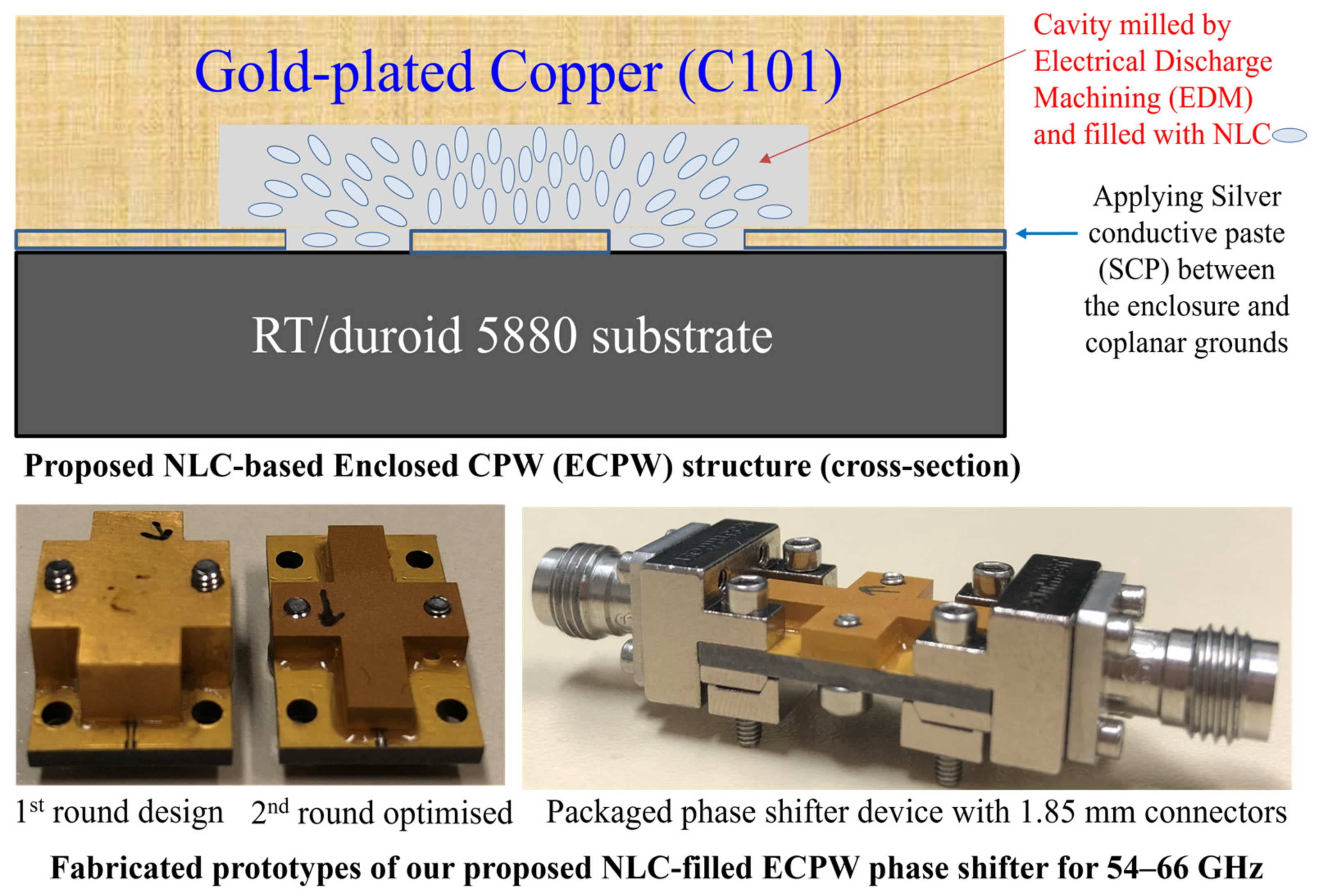
:1. Introduction
2. Materials and Methods
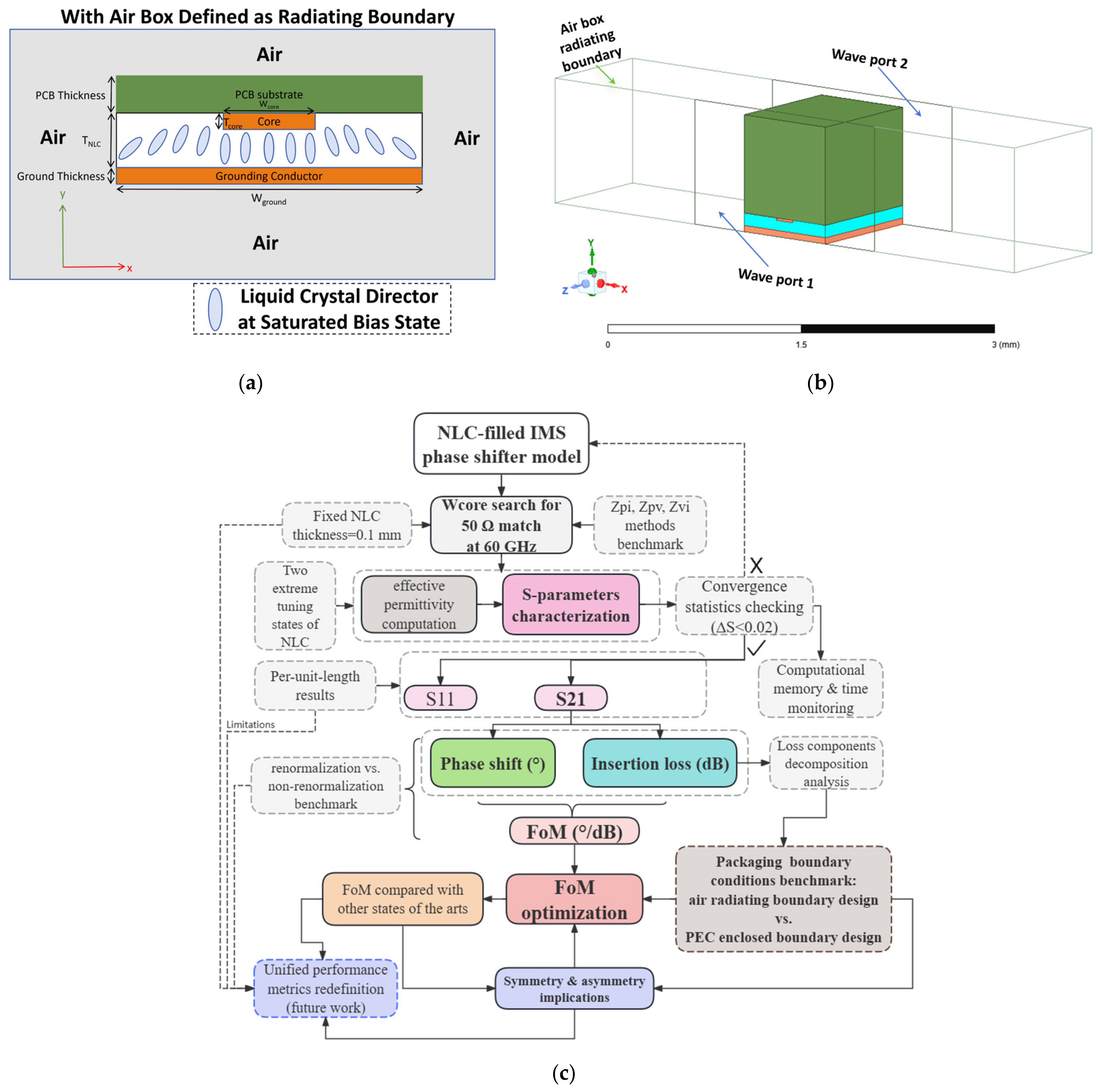
2.1. NLC-IMS Line Model with an Air Box as a Radiating Boundary
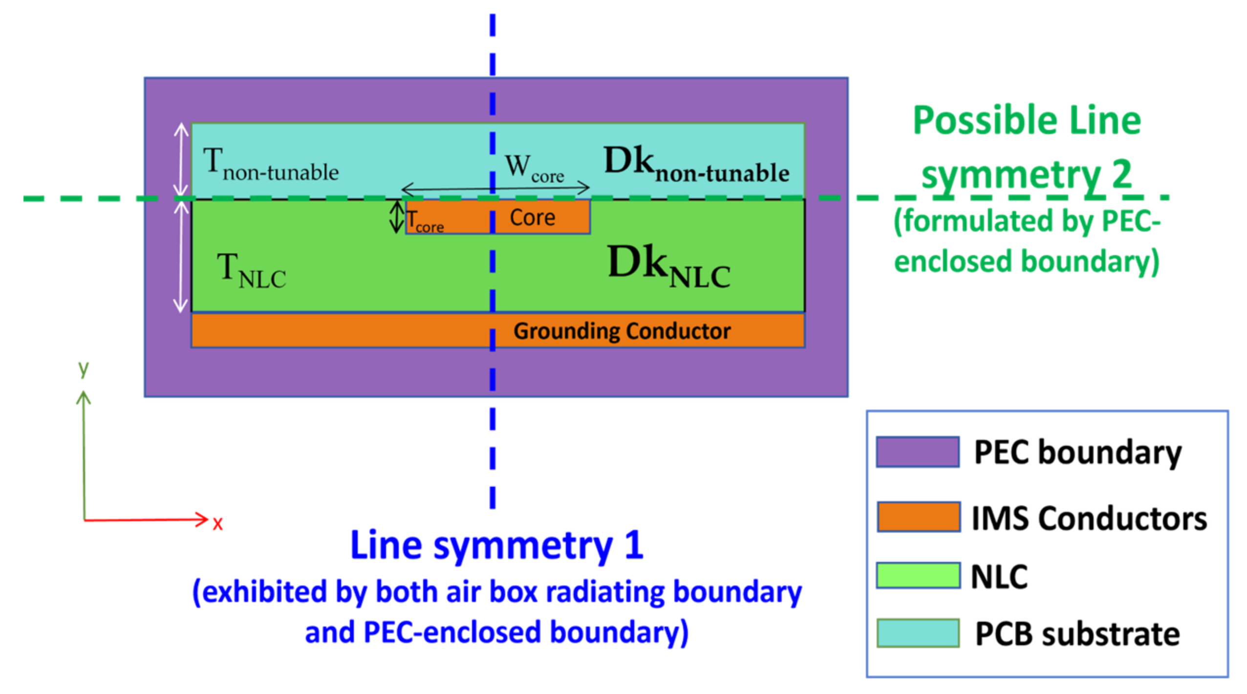
2.2. Air Box Radiating Boundary vs. PEC Enclosed Boundary
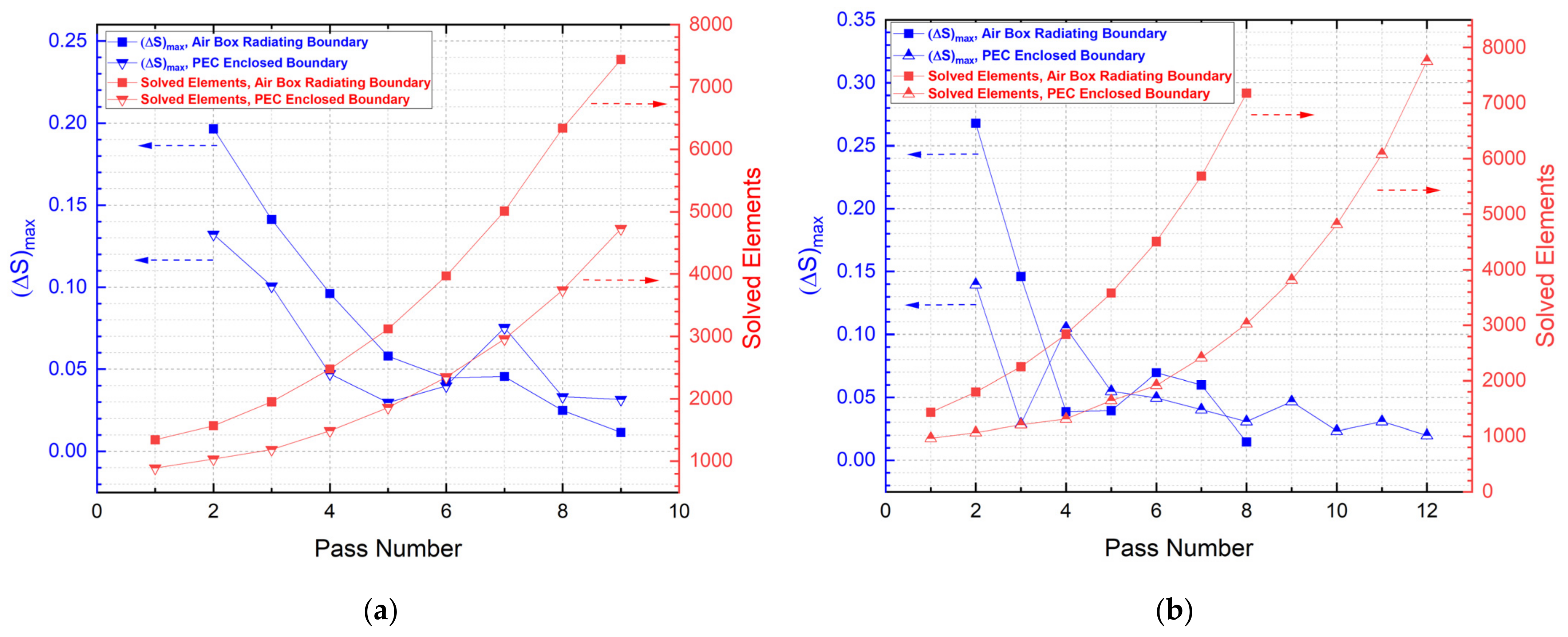
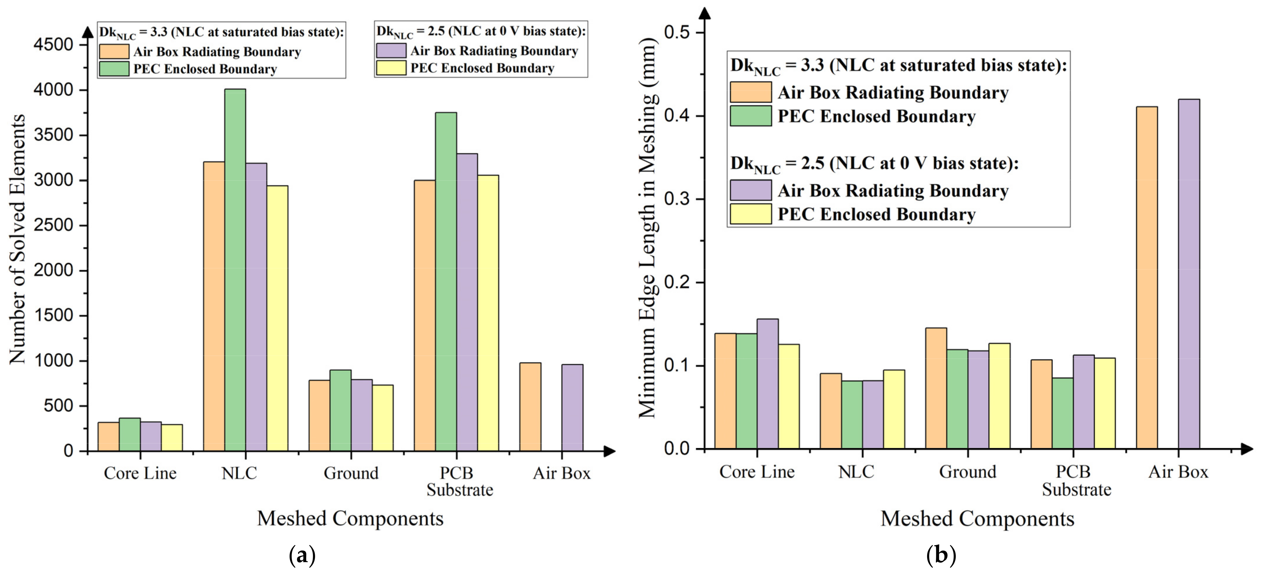
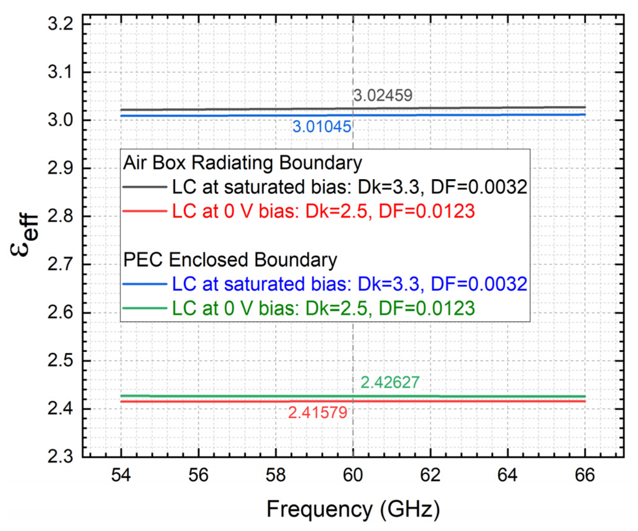
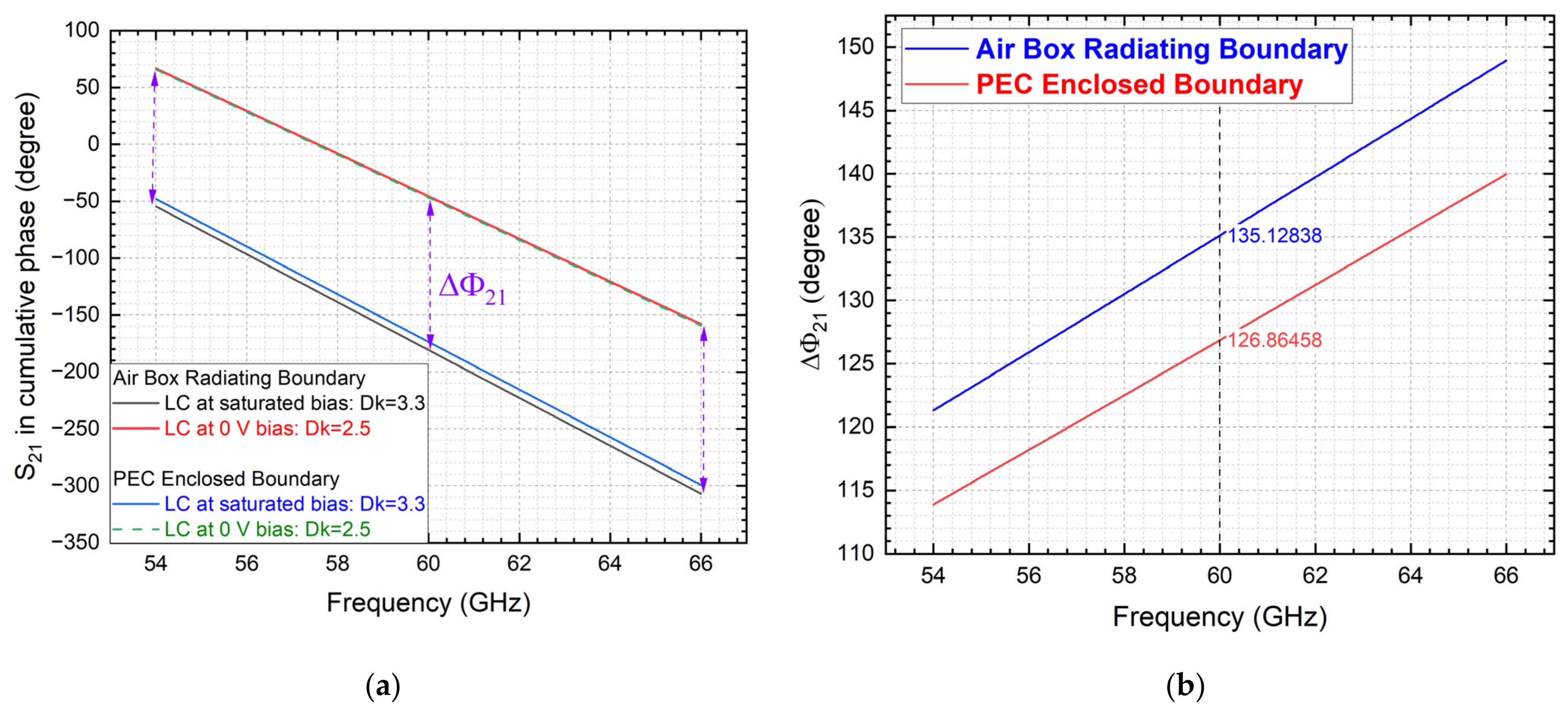
3. Full-wave Numerical Results Benchmark and Verification
3.1. Simulated Phase Shifting Performance
3.2. Loss Element Decomposed Analysis and Benchmark
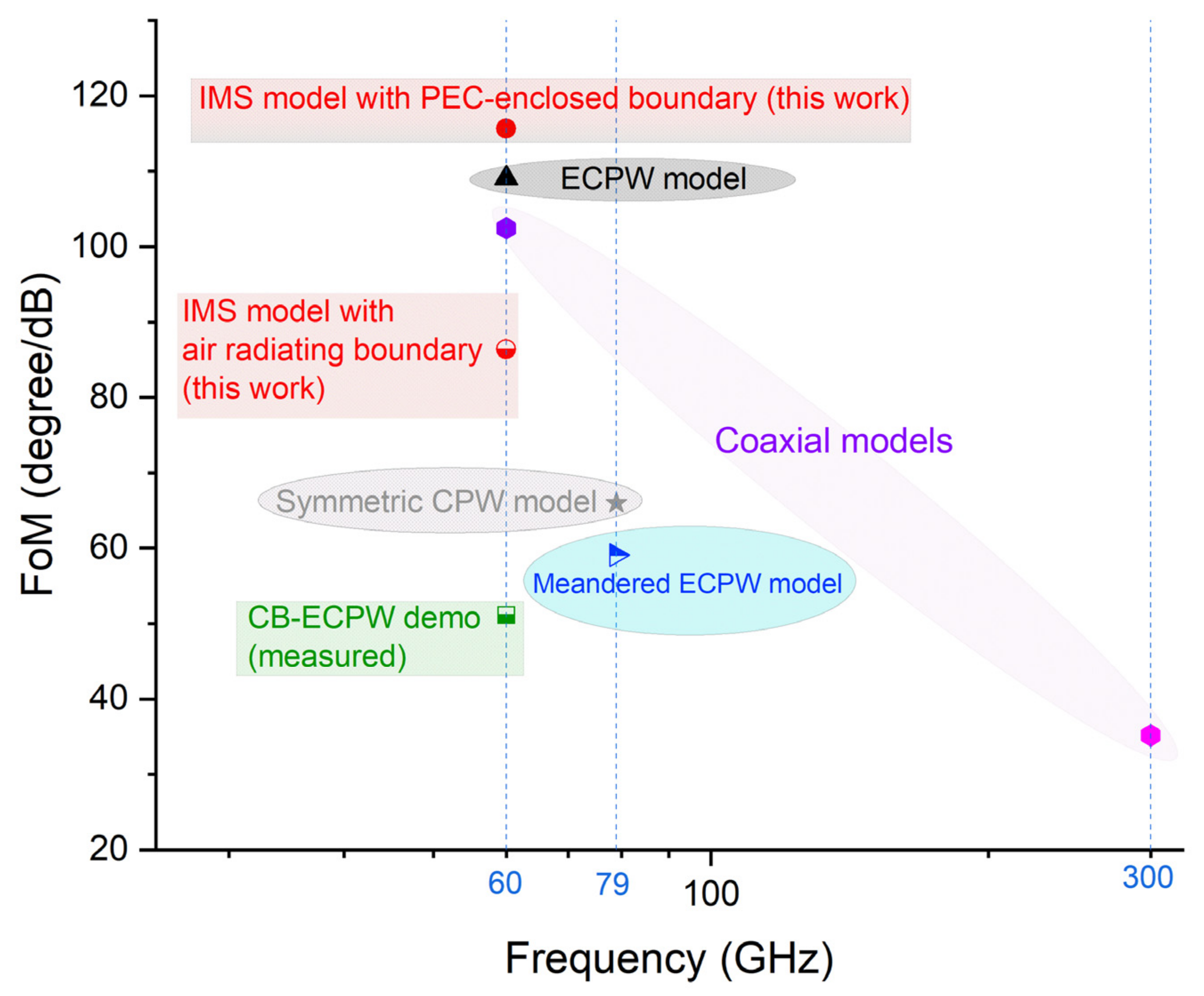
4. Discussions on Advantages and Limitations
4.1. FoM Comparison Numerically with Other Planar and Non-Planar Phase Shifters with NLC
4.2. Rethinking the Optimization Opportunity via Symmetry and Asymmetry
5. Conclusions and Future Research Outlook
Author Contributions
Funding
Data Availability Statement
Conflicts of Interest
Abbreviations
| Nomenclatures | Abbreviations |
| Inverted microstrip line | IMS |
| Figure-of-merit | FoM |
| Liquid crystal | LC |
| Nematic liquid crystal | NLC |
| Liquid crystal display | LCD |
| Coplanar waveguide | CPW |
| Enclosed coplanar waveguide | ECPW |
| Conductor-backed enclosed coplanar waveguide | CB-ECPW |
| Perfect electric conductor | PEC |
| Printed circuit board | PCB |
| Microwave-wave | MW |
| Millimeter-wave | mmW |
| Gigahertz | GHz |
| Terahertz | THz |
| Scattering parameters | S parameters |
| Forward transmission coefficient | S21 |
| Forward reflection coefficient | S11 |
| Dielectric constant | Dk |
| Dissipation factor | DF |
| Three dimensional | 3D |
| Fifth-generation wireless | 5G |
| Sixth-generation wireless | 6G |
| Finite-element method | FEM |
| High-frequency structure simulator | HFSS |
| Polyimide | PI |
References
- Kawamoto, H. The history of liquid-crystal display and its industry. In Proceedings of the 2012 Third IEEE HISTory of ELectro-technology CONference (HISTELCON), Pavia, Italy, 5–7 September 2012; pp. 1–6. [Google Scholar]
- Maune, H.; Jost, M.; Reese, R.; Polat, E.; Nickel, M.; Jakoby, R. Microwave Liquid Crystal Technology. Crystals 2018, 8, 355. [Google Scholar] [CrossRef]
- Zografopoulos, D.C.; Ferraro, A.; Beccherelli, R. Liquid-crystal high-frequency microwave technology: Materials and Characterization. Adv. Mater. Technol. 2018, 4, 1800447. [Google Scholar] [CrossRef]
- Nose, T.; Ito, R.; Honma, M. Potential of Liquid-Crystal Materials for Millimeter-Wave Application. Appl. Sci. 2018, 8, 2544. [Google Scholar] [CrossRef]
- Kowerdziej, R.; Garbat, K.; Walczakowski, M. Nematic liquid crystal mixtures dedicated to thermally tunable terahertz devices. Liq. Cryst. 2018, 45, 1040–1046. [Google Scholar] [CrossRef]
- Dolfi, D.; Labeyrie, M.; Joffre, P.; Huignard, J.P. Liquid crystal microwave phase shifter. Electron. Lett. 1993, 29, 926–928. [Google Scholar] [CrossRef]
- Lim, K.C.; Margerum, J.D.; Lackner, A.M. Liquid crystal millimeter wave electronic phase shifter. Appl. Phys. Lett. 1993, 62, 1065–1067. [Google Scholar] [CrossRef]
- Li, J.; Chu, D. Liquid Crystal-Based Enclosed Coplanar Waveguide Phase Shifter for 54–66 GHz Applications. Crystals 2019, 9, 650. [Google Scholar] [CrossRef]
- Kuki, T.; Fujikake, H.; Nomoto, T.; Utsumi, Y. Design of a microwave variable delay line using liquid crystal, and a study of its insertion loss. Electron. Commun. Jpn. 2002, 85, 36–42. [Google Scholar] [CrossRef]
- Neuder, R.; Späth, M.; Schüßler, M.; Sáez, A.J. Architecture for sub-100 ms liquid crystal reconfigurable intelligent surface based on defected delay lines. Commun. Eng. 2024, 3, 70. [Google Scholar] [CrossRef]
- Kuki, T.; Fujikake, H.; Nomoto, T. Microwave variable delay line using dual-frequency switching-mode liquid crystal. IEEE Trans. Microw. Theory Tech. 2002, 50, 2604–2609. [Google Scholar] [CrossRef]
- De Gennes, P.G.; Prost, J. The Physics of Liquid Crystals; Oxford University Press: Oxford, UK, 1995. [Google Scholar]
- Longzhu, C.; Huan, X.; Jinfeng, L.; Daping, C. High Figure-of-merit compact phase shifters based on liquid crystal material for 1–10 GHz applications. Jpn. J. Appl. Phys. 2017, 56, 011701. [Google Scholar]
- Li, J.; Xu, H.; Chu, D. Design of liquid crystal based coplanar waveguide tunable phase shifter with no floating electrodes for 60–90 GHz applications. In Proceedings of the 2016 46th European Microwave Conference (EuMC), London, UK, 4–6 October 2016; pp. 1047–1050. [Google Scholar]
- Li, J.; Li, H. Liquid Crystal-Filled 60 GHz Coaxially Structured Phase Shifter Design and Simulation with Enhanced Figure of Merit by Novel Permittivity-Dependent Impedance Matching. Electronics 2024, 13, 626. [Google Scholar] [CrossRef]
- Li, J.; Li, H. Modeling 0.3 THz Coaxial Single-Mode Phase Shifter Designs in Liquid Crystals with Constitutive Loss Quantifications. Crystals 2024, 14, 364. [Google Scholar] [CrossRef]
- Ennajih, A.; Sardi, A.; Sadik, M.; Zbitou, J. Design and Analysis of Intelligent Reflecting Surface for 5G Applications. In Proceedings of the 2023 10th International Conference on Wireless Networks and Mobile Communications (WINCOM), Istanbul, Turkiye, 26–28 October 2023; pp. 1–5. [Google Scholar]
- Abdalmalak, K.A.; Santamaría Botello, G.; Llorente-Romano, S.; Rivera-Lavado, A.; Flygare, J.; López Fernándezs, J.A.; Serna Puente, J.M.; García-Castillo, L.E.; Segovia-Vargas, D.; Pantaleev, M.; et al. Ultrawideband Conical Log-Spiral Circularly Polarized Feed for Radio Astronomy. IEEE Trans. Antennas Propag. 2020, 68, 1995–2007. [Google Scholar] [CrossRef]
- Jakoby, R.; Gaebler, A.; Weickhmann, C. Microwave Liquid Crystal Enabling Technology for Electronically Steerable Antennas in SATCOM and 5G Millimeter-Wave Systems. Crystals 2020, 10, 514. [Google Scholar] [CrossRef]
- Li, J. Rethinking Liquid Crystal Tunable Phase Shifter Design with Inverted Microstrip Lines at 1–67 GHz by Dissipative Loss Analysis. Electronics 2023, 12, 421. [Google Scholar] [CrossRef]
- Li, X.; Jiao, Y.C.; Zhang, L. Wideband low-profile CPW-fed slot-loop antenna using an artificial magnetic conductor. Electron. Lett. 2018, 54, 673–674. [Google Scholar] [CrossRef]
- Abdulkarim, Y.I.; Deng, L.; Karaaslan, M.; Altıntaş, O.; Awl, H.N.; Muhammadsharif, F.F.; Liao, C.; Unal, E.; Luo, H. Novel Metamaterials-Based Hypersensitized Liquid Sensor Integrating Omega-Shaped Resonator with Microstrip Transmission Line. Sensors 2020, 20, 943. [Google Scholar] [CrossRef]
- Marini, S.E.; Zbitou, J.; Mandry, R.; Errkik, A.; Tajmouati, A.; Latrach, M. Design of 45 degree microstrip phase shifter for beam forming network application using parallel coupled lines. In Proceedings of the 2017 International Conference on Wireless Technologies, Embedded and Intelligent Systems (WITS), Fez, Morocco, 19–20 April 2017; pp. 1–3. [Google Scholar]
- Massoni, E.; Bozzi, M.; Perregrini, L.; Tamburini, U.A.; Tomassoni, C. A novel class of high dielectric resonator filters in microstrip line technology. In Proceedings of the 2017 IEEE MTT-S International Microwave Workshop Series on Advanced Materials and Processes for RF and THz Applications (IMWS-AMP), Pavia, Italy, 20–22 September 2017; pp. 1–3. [Google Scholar]
- Oukaira, A.; Said, D.; Zbitou, J.; Lakhssassi, A. Advanced Thermal Control Using Chip Cooling Laminate Chip (CCLC) with Finite Element Method for System-in-Package (SiP) Technology. Electronics 2023, 12, 3154. [Google Scholar] [CrossRef]
- Alam, B.; Cornaggia, F.; Alessandro, A.; Asquini, R. Design and analysis of high performance phase shifters on polymeric slot waveguides within liquid crystal cladding. Opt. Quant. Electron. 2022, 54, 800. [Google Scholar] [CrossRef]
- Cornaggia, F.; Alam, B.; Alessandro, A.; Asquini, R. Analysis of a phase shifter based on a slot polymeric waveguide with liquid crystal cladding. In Proceedings of the 2021 International Conference on Numerical Simulation of Optoelectronic Devices (NUSOD), Turin, Italy, 13–17 September 2021; pp. 107–108. [Google Scholar]
- Li, J. Towards 76–81 GHz Scalable Phase Shifting by Folded Dual-strip Shielded Coplanar Waveguide with Liquid Crystals. Ann. Emerg. Technol. Comput. 2021, 5, 14–22. [Google Scholar] [CrossRef]
- Tesmer, H.; Razzouk, R.; Polat, E.; Wang, D.; Jakoby, R.; Maune, H. Temperature Characterization of Liquid Crystal Dielectric Image Line Phase Shifter for Millimeter-Wave Applications. Crystals 2021, 11, 63. [Google Scholar] [CrossRef]
- Nose, T.; Ito, T.; Ito, R.; Honma, M. Basic Performance of Rectangular Waveguide Type Liquid Crystal Phase Shifter Driven by Magnetic Field. In Proceedings of the 2018 43rd International Conference on Infrared, Millimeter, and Terahertz Waves (IRMMW-THz), Nagoya, Japan, 9–14 September 2018; pp. 1–2. [Google Scholar]
- Chen, C.Y.; Hsieh, C.F.; Lin, Y.F.; Pan, R.P.; Pan, C.L. Magnetically tunable room-temperature 2π liquid crystal terahertz phase shifter. Opt. Express 2004, 12, 2625–2630. [Google Scholar] [CrossRef]
- Ishihara, S.; Uto, S. Symmetry and Liquid Crystals. Symmetry 2023, 15, 691. [Google Scholar] [CrossRef]
- Zid, M.; Pal, K.; Harkai, S.; Abina, A.; Kralj, S.; Zidanšek, A. Qualitatively and Quantitatively Different Configurations of Nematic–Nanoparticle Mixtures. Nanomaterials 2024, 14, 436. [Google Scholar] [CrossRef]
- Repnik, R.; Ranjkesh, A.; Simonka, V.; Ambrozic, M.; Bradac, Z.; Kralj, S.J. Symmetry breaking in nematic liquid crystals: Analogy with cosmology and magnetism. J. Phys. Condens. Matter 2013, 25, 404201. [Google Scholar] [CrossRef]
- Yamaguchi, R. Analysis of Electro-Optical Behavior in Liquid Crystal Cells with Asymmetric Anchoring Strength. Symmetry 2022, 14, 85. [Google Scholar] [CrossRef]
- Bryan-Brown, G.P.; Wood, E.L.; Sage, I.C. Weak surface anchoring of liquid crystals. Nature 1999, 399, 338–340. [Google Scholar] [CrossRef]
- Li, X.; Yanagimachi, T.; Bishop, C.; Smith, C.; Dolejsi, M.; Xie, H.; Kurihara, K.; Nealey, P.F. Engineering the anchoring behavior of nematic liquid crystals on a solid surface by varying the density of liquid crystalline polymer brushes. Soft Matter 2018, 14, 7569–7577. [Google Scholar] [CrossRef]
- Choi, Y.; Oh, S.-W.; Choi, T.-H.; Sohn, H.-J.; Do, S.-M.; Yoon, T.-H. Liquid crystal cell asymmetrically anchored for high transmittance and triggered with a vertical field for fast switching. Opt. Express 2020, 28, 20553–20562. [Google Scholar] [CrossRef]
- Zhang, R.; Roberts, T.; Aranson, I.S.; Pablo, J.J. Lattice Boltzmann simulation of asymmetric flow in nematic liquid crystals with finite anchoring. J. Chem. Phys. 2016, 144, 084905. [Google Scholar] [CrossRef] [PubMed]
- Bezrukov, A.; Galyametdinov, Y. Orientation Behavior of Nematic Liquid Crystals at Flow-Wall Interfaces in Microfluidic Channels. Coatings 2023, 13, 169. [Google Scholar] [CrossRef]
- Sengupta, A.; Tkalec, U.; Ravnik, M.; Yeomans, J.M.; Bahr, C.; Herminghaus, S. Liquid crystal microfluidics for tunable flow shaping. Phys. Rev. Lett. 2013, 110, 048303. [Google Scholar] [CrossRef] [PubMed]


| Geometry Items (Materials) | Width (x-Axis) | Thickness (y-Axis) | Length (z-Axis) |
|---|---|---|---|
| Grounding Conductor (Cu) | Wground = 5 Wcore | Tground = 0.05 mm | 1 mm |
| Filled NLC Dielectric (GT3-24002) | 5 Wcore | TLC = 0.1 mm | 1 mm |
| Core Conductor (Cu) | Wcore | Tcore = 0.018 mm | 1 mm |
| PCB Substrate (RT 5880) | WPCB = 5 Wcore | TPCB = 0.787 mm | 1 mm |
| Boundary Designs and Tuning States | Maximum Memory/Process | Average Memory/Process | Elapsed Time |
|---|---|---|---|
| Air box radiating boundary, NLC Dk = 3.3 | 260 MB | 259 MB | 00:04:54 |
| Air box radiating boundary, NLC Dk = 2.5 | 271 MB | 271 MB | 00:04:49 |
| PEC enclosed boundary, NLC Dk = 3.3 | 243 MB | 243 MB | 00:06:04 |
| PEC enclosed boundary, NLC Dk = 2.5 | 187 MB | 186 MB | 00:06:05 |
Disclaimer/Publisher’s Note: The statements, opinions and data contained in all publications are solely those of the individual author(s) and contributor(s) and not of MDPI and/or the editor(s). MDPI and/or the editor(s) disclaim responsibility for any injury to people or property resulting from any ideas, methods, instructions or products referred to in the content. |
© 2024 by the authors. Licensee MDPI, Basel, Switzerland. This article is an open access article distributed under the terms and conditions of the Creative Commons Attribution (CC BY) license (https://creativecommons.org/licenses/by/4.0/).
Share and Cite
Li, J.; Li, H. Symmetry Implications of a 60 GHz Inverted Microstrip Line Phase Shifter with Nematic Liquid Crystals in Diverse Packaging Boundary Conditions. Symmetry 2024, 16, 798. https://doi.org/10.3390/sym16070798
Li J, Li H. Symmetry Implications of a 60 GHz Inverted Microstrip Line Phase Shifter with Nematic Liquid Crystals in Diverse Packaging Boundary Conditions. Symmetry. 2024; 16(7):798. https://doi.org/10.3390/sym16070798
Chicago/Turabian StyleLi, Jinfeng, and Haorong Li. 2024. "Symmetry Implications of a 60 GHz Inverted Microstrip Line Phase Shifter with Nematic Liquid Crystals in Diverse Packaging Boundary Conditions" Symmetry 16, no. 7: 798. https://doi.org/10.3390/sym16070798
APA StyleLi, J., & Li, H. (2024). Symmetry Implications of a 60 GHz Inverted Microstrip Line Phase Shifter with Nematic Liquid Crystals in Diverse Packaging Boundary Conditions. Symmetry, 16(7), 798. https://doi.org/10.3390/sym16070798