Article

A Design Approach for Asymmetric Coupled Line In-Phase Power Dividers with Arbitrary Terminal Real Impedances and Arbitrary Power Division Ratio

State Key Laboratory of Radio Frequency Heterogeneous Integration, Shanghai Jiao Tong University, Shanghai 200240, China
*
Author to whom correspondence should be addressed.
Symmetry 2025, 17(4), 562; https://doi.org/10.3390/sym17040562
Submission received: 9 March 2025 / Revised: 1 April 2025 / Accepted: 7 April 2025 / Published: 8 April 2025

Abstract

:
In this paper, we first introduced asymmetric coupled lines (ACLs) into both the transmission path and isolation path in traditional in-phase Gysel power dividers and proposed the single-resistor asymmetric coupled line in-phase Gysel power dividers (ACPDs). Utilizing the decoupled branch-line model of ACLs, a generalized design approach for ACPDs with arbitrary terminal real impedances and arbitrary power division ratio was innovatively proposed. Design formulas relating terminal real impedances, power division ratio, and image impedances of ACLs, for simultaneously satisfying the perfect port isolation and match conditions, are presented. ACPDs achieved a large in-phase power division ratio of 100:1 (20 dB) and offered significant advantages, including impedance transformation, high design freedom, and miniaturization. To automatically determine accurate initial values of geometric parameters for ACLs, a solution software based on MATLAB-HFSS co-simulation and multi-layer perception neural networks was developed, significantly reducing subsequent optimization iterations. To verify the proposed analysis theory and design approach, three ACPDs with different power division ratios of 1:1 (3 dB), 10:1 (10 dB), and 100:1 (20 dB) were implemented. Comparisons of the measured and simulated results showed great accordance, and the three ACPDs achieved good frequency bandwidth, high isolation, excellent port match, and compact size.

1. Introduction

With the development of wireless technology, improving design freedom and reducing optimization iterations have become critical issues for engineers. In practical design, increasing the number of adjustable geometric parameters of components is an effective method to achieve higher design freedom. Consequently, compared to symmetric structures, the importance of asymmetric structures, such as asymmetric coupled lines, is gradually emerging.
As a fundamental unit in the field of RF and microwave engineering, coupled lines possess a compact structure and broad bandwidth, making them widely utilized in couplers [1], power dividers [2], filters [3], antennas [4], power amplifiers [5], etc. Compared to the extensively adopted symmetric coupled lines (SCLs), the asymmetric coupled line (ACL) structure [6] offers two significant advantages.
  • Firstly, ACL provides an additional line width variable, allowing for more design freedom.
  • Secondly, the terminal real impedances of ACL devices can simultaneously take on different values, endowing them with the capability of impedance transformation and expanding the application space of devices.
Although the analysis and design of ACLs are relatively complex due to the difficulty of decoupling and the lack of empirical formulas, we have successfully established an effective branch-line decoupled model of ACLs using the method of N-port network equivalence in [7].
As a classic type of power divider, Gysel power dividers boast higher power capability than Wilkinson power dividers by introducing two short-ended resistors to transfer heat to the ground plane. In modern RF circuits, key concerns for a Gysel power divider include achieving arbitrary and large power division ratios (PDRs) [8,9], impedance transformation, compact size, multi-band [10], and broad bandwidth. Various methods, such as phase inverters [11], electromagnetic bandgap (EBG) structures [12], coupled lines [10,13,14], and open or short stubs [15,16], have been employed to meet some of these requirements. In [13], the proposed in-phase Gysel power divider with one isolation resistor saves circuit space by eliminating the 180° electrical length transmission line and incorporating a quarter-wavelength SCL section. However, this design cannot accommodate impedance transformation, achieves a relatively small PDR, and still requires two isolation resistors in the equal power division case. Generally, achieving a large in-phase PDR is challenging, and an in-phase PDR of more than 10 dB is rarely reported in the literature.
In this paper, to explore the advantages of ACLs for impedance transformation, large PDR, and miniaturization of power dividers, we innovatively proposed the asymmetric coupled line in-phase Gysel power dividers (ACPDs). The ACPDs require only one isolation resistor for both equal and unequal power division cases. Through detailed analysis of the isolation path and power dividing path in an N-port network, combined with the decoupled branch-line model of ACLs at the central frequency, the relationships between terminal real impedances, image impedances (defined by the decoupled model of ACLs), and PDR to meet the conditions for perfect port match and isolation are established. To reduce the design difficulty, an automatic solution software developed using MATLAB (R2020b)-HFSS (2021R1) co-simulation and multi-layer perception neural networks to determine accurate values of geometric parameters for ACLs was developed. For verification, three single-resistor ACPDs with PDRs (dB) of 3 dB, 10 dB, and 20 dB were implemented. For the first time, our proposed ACPD achieved a large PDR of 20 dB. The remarkable consistency between simulated and measured data strongly supports the validity of the proposed design approach and highlights the flexibility and performance advantages of ACLs.
This paper is organized as follows: Section 2 introduces the theoretical analysis and design methodology for ACPDs. The principle and processing procedures of the automatic solution software are presented in Section 3. The performance of the three fabricated ACPDs is shown in Section 4. Section 5 discusses the application of devices with arbitrary terminal real impedances and arbitrary power division ratios. Section 6 concludes the whole paper.

2. Theoretical Analysis and Design Methodology

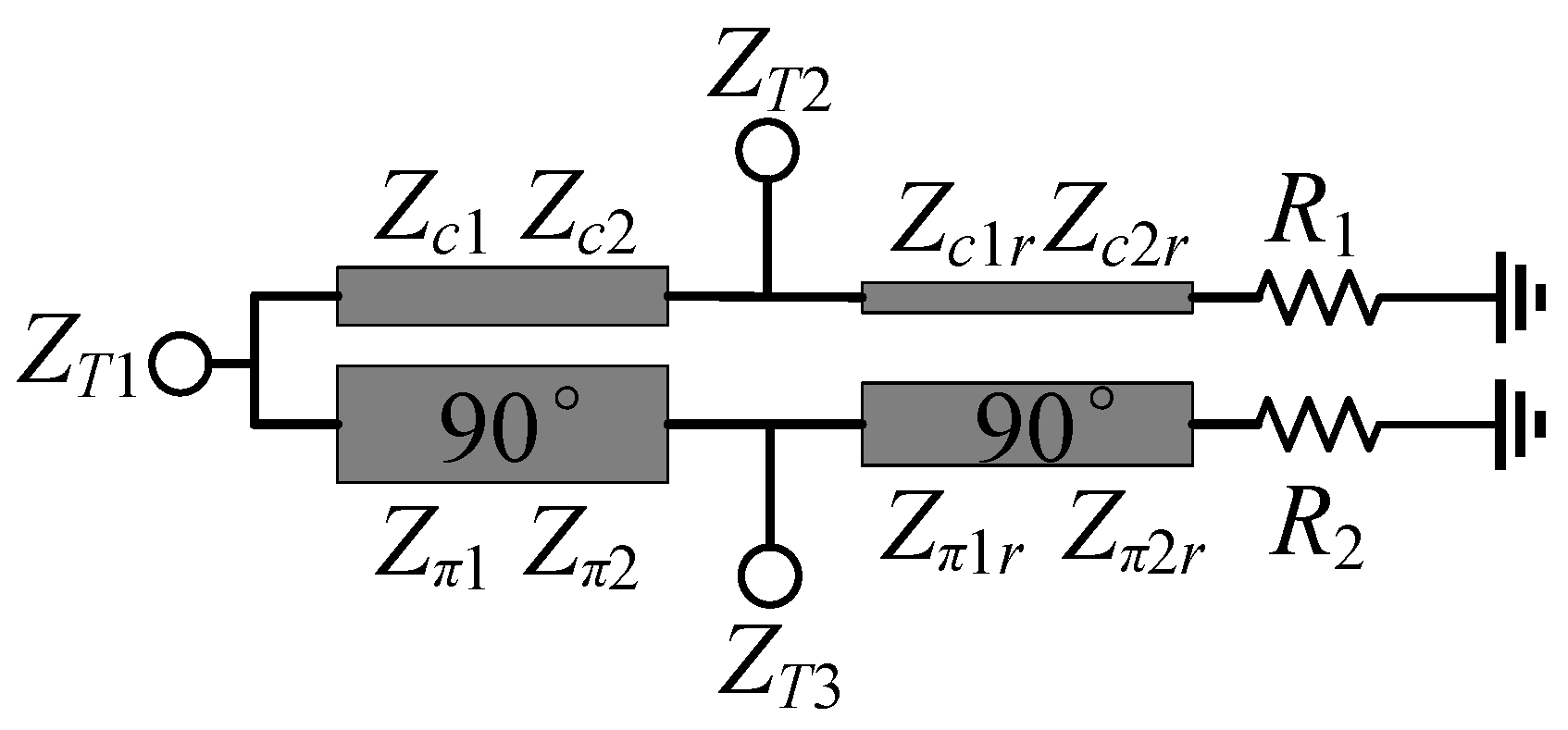
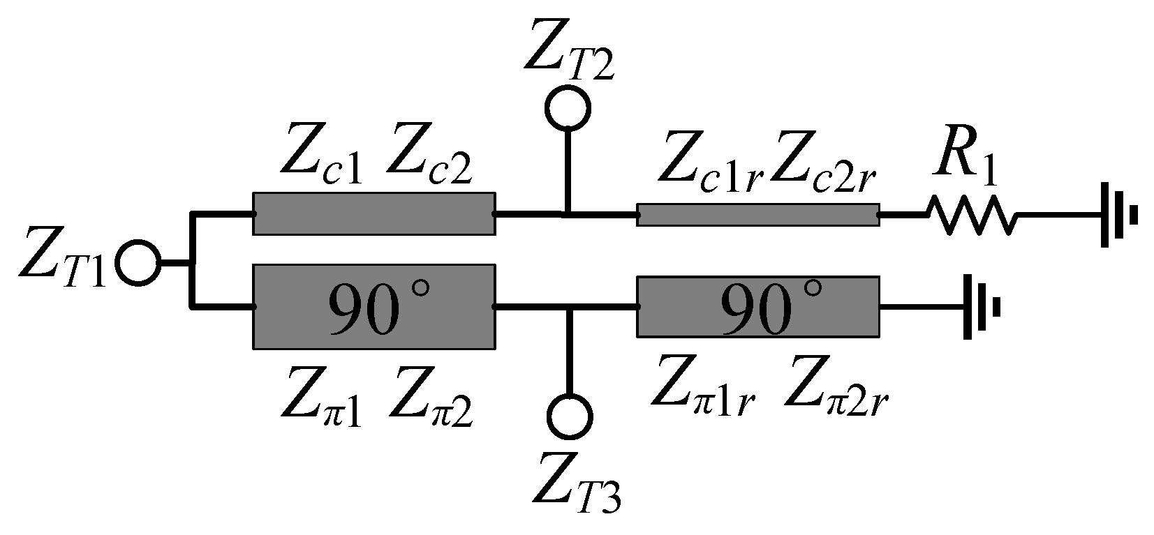
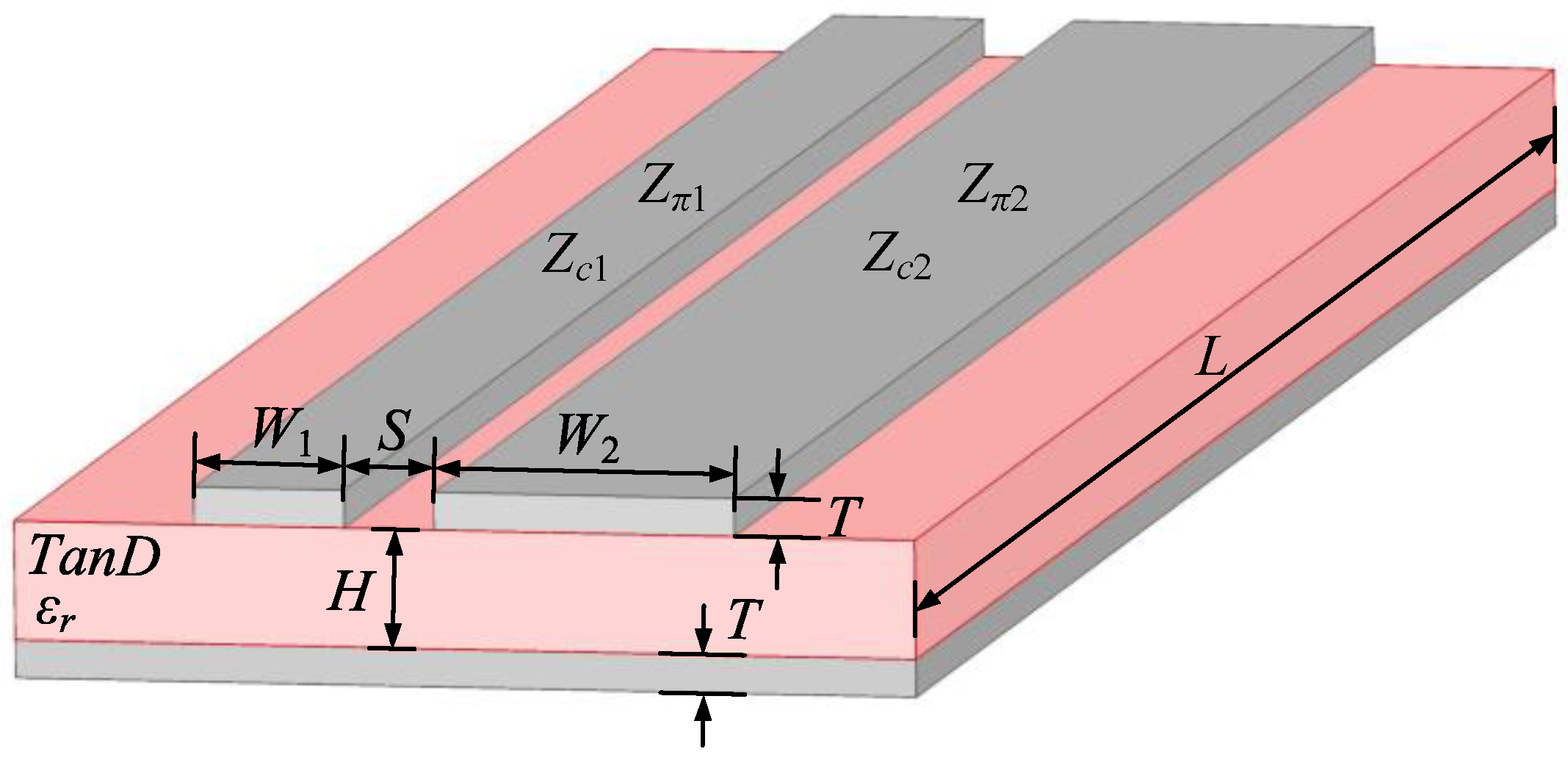
2.1. Two-Resistor APCD Structure

The prototype of the proposed ACPD is shown in Figure 1. This design features two sections of quarter-wavelength ACLs, each with different geometric parameter values and, respectively, constituting the transmission path and part of the isolation path of ACPD. To enhance the universality of the following analysis, it is initially assumed that the ACPD includes two isolation resistors R1 and R2. The terminal real impedances of ACPD are denoted as ZT1, ZT2, and ZT3. Utilizing the decoupled branch-line model of ACLs at the central frequency proposed in [7], the decoupled circuit of the ACPD is presented in Figure 2. Here, ZI1 to ZI4 represents the image impedances of the left ACL section, while ZI1r to ZI4r are the image impedances of the right one.
For the ACPD shown in Figure 2, there is one ideal isolation condition between ports T2 and T3. Consider the 2-port subnetwork constituted by ports T2 and T3 as shown in Figure 3, which consists of three subcircuits A, B, and C in parallel. Their corresponding admittance matrices, YA, YB, and YC, are as follows:
Y A = 1 G 1 Z I 1 r 2 1 G 1 Z I 1 r Z I 4 r 1 G 1 Z I 1 r Z I 4 r 1 G 1 Z I 4 r 2 ,
Y B = 1 G 2 Z I 2 r 2 1 G 2 Z I 2 r Z I 3 r 1 G 2 Z I 2 r Z I 3 r 1 G 2 Z I 3 r 2 ,
Y C = ( Y I 4 Y I 1 ) 2 Y T 1 ( Y I 1 Y I 4 ) ( Y I 3 Y I 2 ) Y T 1 ( Y I 1 Y I 4 ) ( Y I 3 Y I 2 ) Y T 1 ( Y I 2 Y I 3 ) 2 Y T 1 ,
where G1 = R1−1, and G2 = R2−1. Then, the overall admittance matrix YT2T3 is obtained as follows:
Y T 2 T 3 = Y A + Y B + Y C = Y 11 Y 12 Y 21 Y 22 ,
where
Y 11 = 1 G 1 Z I 1 r 2 + 1 G 2 Z I 2 r 2 + ( Y I 4 Y I 1 ) 2 Y T 1 Y 12 = 1 G 1 Z I 1 r Z I 4 r 1 G 2 Z I 2 r Z I 3 r + ( Y I 1 Y I 4 ) ( Y I 3 Y I 2 ) Y T 1 = Y 21 Y 22 = 1 G 1 Z I 4 r 2 + 1 G 2 Z I 3 r 2 + ( Y I 2 Y I 3 ) 2 Y T 1 .
If the perfect isolation between ports T2 and T3 is realized, the matrix YT2T3 should satisfy that [7],
Y T 2 T 3 = Y 11 Y 12 Y 21 Y 22 = Y T 2 0 0 Y T 3 .
Then, one set of equations is obtained from (4) to (6) as follows:
R 1 Z I 1 r 2 + R 2 Z I 2 r 2 + ( Y I 4 Y I 1 ) 2 Y T 1 = Y T 2 R 1 Z I 4 r 2 + R 2 Z I 3 r 2 + ( Y I 2 Y I 3 ) 2 Y T 1 = Y T 3 R 1 Z I 1 r Z I 4 r + R 2 Z I 2 r Z I 3 r = ( Y I 1 Y I 4 ) ( Y I 3 Y I 2 ) Y T 1 .
Now, consider the power transmission between ports T1, T2, and T3. When the input port T1 is excited, in an ideal case, the input power is transmitted entirely to output ports T2 and T3, with no current flowing into resistors R1 and R2. Figure 4 shows the simplified circuit of ACPD for the power analysis, with the definition of node voltages and currents. Based on voltage–current relation, there are
V 1 = j Y I 1 Y I 4 I 2 = j Y I 1 Y I 4 V 2 Z T 2 I a = j ( Y I 1 Y I 4 ) V 2 ,
V 1 = j Y I 3 Y I 2 I 3 = j Y I 3 Y I 2 V 3 Z T 3 I b = j ( Y I 3 Y I 2 ) V 3 .
By the definition of the power division ratio Rp = PT2/PT3, as well as the law of power conservation, the following set of equations is obtained:
Z T 2 ( Y I 1 Y I 4 ) 2 + Z T 3 ( Y I 3 Y I 2 ) 2 = 1 Z T 1 1 Z T 3 Z T 1 ( Y I 3 Y I 2 ) 2 1 = r p .
Set ZT2 = xZT1, ZT3 = yZT1, ZI1 = K1ZT1, ZI2 = ZI4 = K2ZT1, ZI3 = K3ZT1, ZI1r = K4ZT1, ZI2r = ZI4r = K5ZT1, ZI3r = K6ZT1, R1 = t1ZT1, and R2 = t2ZT1, where x, y, t1, and t2 are the arbitrary real coefficients can be realized, and substitute these equations into (7) and (10), there are,
1 K 3 1 K 2 = 1 y ( R p + 1 ) ,   1 K 1 1 K 2 = R p x ( R p + 1 ) ,   t 1 K 4 2 + t 2 K 5 2 = 1 x ( R p + 1 ) t 1 K 5 2 + t 2 K 6 2 = R p y ( R p + 1 ) ,   t 1 K 4 K 5 + t 2 K 2 K 3 = 1 R p + 1 R p x y .
To solve the equations in Equation (11), and relations are obtained as follows:
K 1 = 1 R p x ( R p + 1 ) + 1 K 2 ,   K 3 = 1 1 y ( R p + 1 ) + 1 K 2 ,   K 4 = t 1 1 x ( R p + 1 ) t 2 K 5 2 K 5 = t 2 x ( R p + 1 ) + t 1 y ( R p + 1 ) R p ,   K 6 = t 2 R p y ( R p + 1 ) t 1 K 5 2 .
So far, the relationships between ZIi (i = 1, 2, 3, 4), ZIjr (j = 1, 2, 3, 4), ZT1, ZT2, ZT3, R1, R2, and Rp, for achieving perfect isolation, perfect port match, and power division requirement of the two-resistor ACPDs have been completely deduced and established. It is important to note that, in addition to the values of ZT1, x, y, t1, t2, and Rp, the value of K2 also needs to be specified according to the application requirements, introducing an additional degree of design freedom.
In particular, consider cases of equal power division and equal terminal real impedances. Substitute Rp = 1 and x = y into (12), there are,
K 1 = K 3 = 1 2 x + 1 K 2 1 K 4 = K 5 = K 6 = 2 x ( t 1 + t 2 ) ,
then we have ZI1 = ZI3 and ZI1r = ZI2r = ZI3r. It is noted that, for a physically achievable SCL or ACL section, the value of ZI2 (ZI2r) is always greater than the values of ZI1 (ZI1r) and ZI3 (ZI3r) [7], meaning K2 > K1, K2 > K3, K5 > K4, and K5 > K6. The calculation formulas of ZI1 (ZI1r), ZI2 (ZI2r), and ZI3 (ZI3r) are listed in Section 3 as (20). Therefore, under conditions of perfect isolation and match, it is not possible to simultaneously achieve both equal power division and equal terminal real impedances of the two output ports. However, within a reasonable range, some impedance match and isolation performance can be sacrificed to achieve equal power division and equal terminal impedance at the same time.

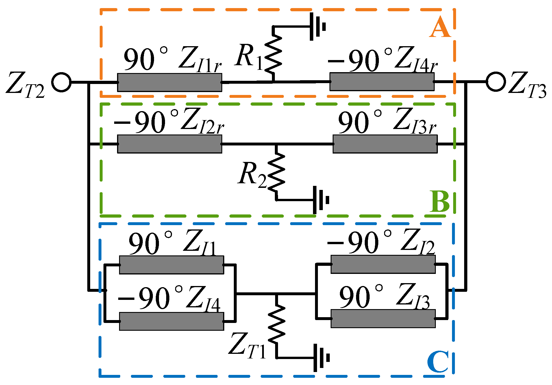
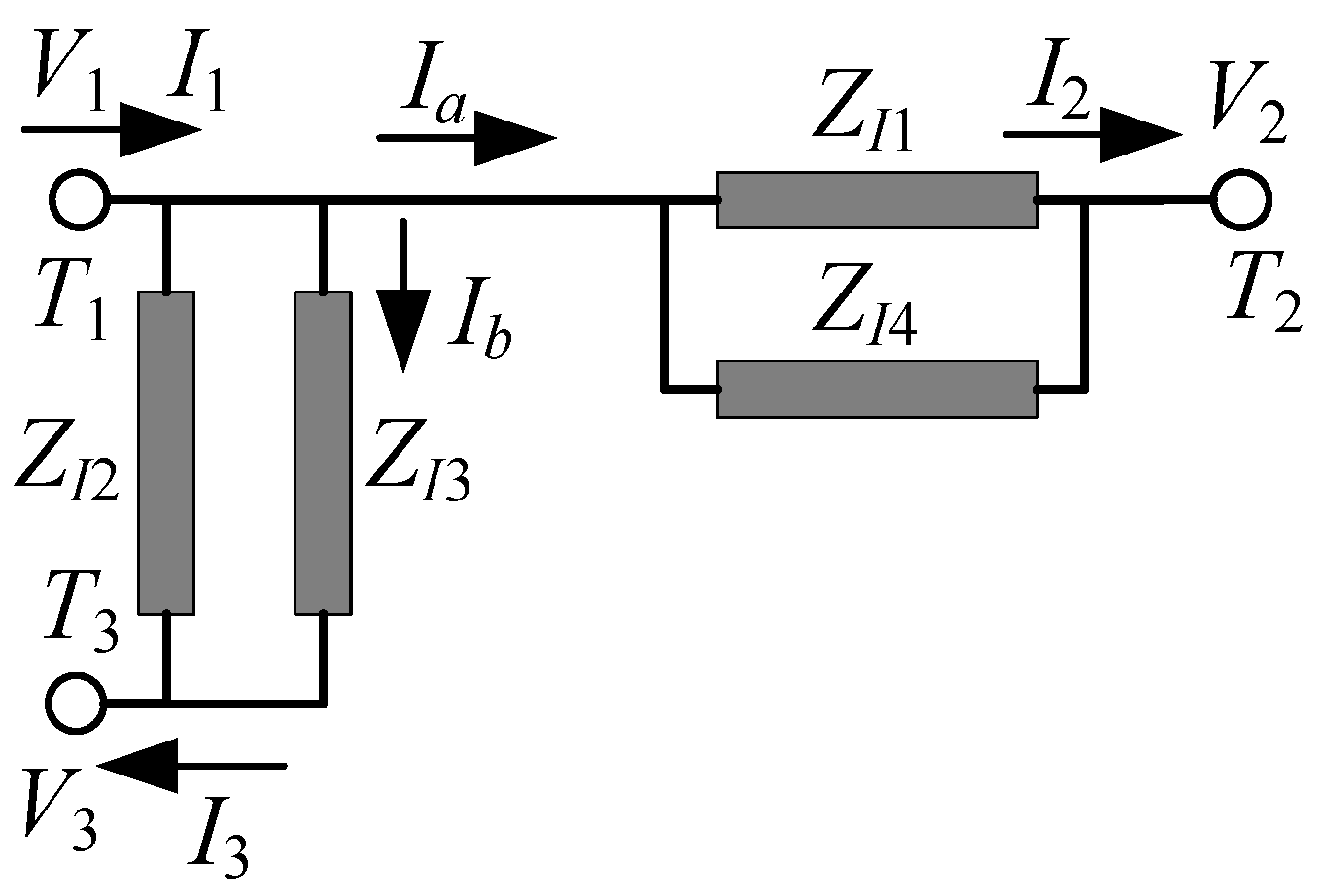
2.2. Single-Resistor APCD Structure

Next, consider the structure of ACPD with only one isolation resistor R1, as shown in Figure 5. Compared with the two-resistor ACPD structure in Figure 1, this ACPD structure reduces design complicity and saves circuit space. Substitute t2 = 0 into (12), there is,
1 K 3 1 K 2 = 1 y ( R p + 1 ) ,   1 K 1 1 K 2 = R p x ( R p + 1 ) t 1 K 4 2 = 1 x ( R p + 1 ) ,   t 1 K 5 2 = R p y ( R p + 1 ) .
By solving Equation (14), relationships are obtained as follows:
K 1 = 1 R p x ( R p + 1 ) + 1 K 2 ,   K 3 = 1 1 y ( R p + 1 ) + 1 K 2 K 4 = t 1 x ( R p + 1 ) ,   K 5 = t 1 y ( R p + 1 ) R p .
So far, the relationships between ZIi (i = 1, 2, 3, 4), ZIjr (j = 1, 2, 3, 4), ZT1, ZT2, ZT3, R1, and Rp, for achieving perfect isolation and port match, and the power division requirement of the single-resistor ACPD have been fully deduced and established. It is noted that, in addition to the values of ZT1, x, y, t1, and Rp, the values of K2 and K6 also need to be specified, providing two additional degrees of design freedom.
For the cases of equal power division and equal terminal real impedances, substituting Rp = 1 and x = y into (15), there are,
K 1 = K 3 = 1 2 x + 1 K 2 1
K 4 = K 5 = 2 x t 1
Clearly, it is physically impossible for both ACLs and SCLs to satisfy Equation (17). Therefore, similar to the two-resistor ACPD analyzed in Section 2.1, under conditions of perfect isolation and match, simultaneously achieving equal power division and equal terminal real impedances cannot be realized by the single-resistor ACPD.
In addition, for the cases of unequal power division, the values of Rp can either be greater than or less than 1. If Rp > 1, since the difference between the values of x and y is generally small, Equation (15) suggests that K5 < K4, which is also physically impossible. Conversely, if Rp < 1, it is straightforward to achieve K5 > K4. Therefore, practically speaking, for the single-resistor ACPD in Figure 4, under conditions of unequal power division, Rp must be less than 1, indicating that the power transmitted to port T2 is smaller than that transmitted to port T3.
Then, consider the cases of a large power division ratio. Substitute Rp ≈ 0 into (15), there are,
K 1 K 2 ,   K 3 = 1 y + 1 K 2 1 K 4 = x t ,   K 5 + . ,
It is known that the larger the line spacing, the greater ZI2 (ZI2r) [7], and the larger K2 (K5). Thus, to satisfy conditions of K1 = K2 and K5 ≈ +∞, the line spacing of the left ACL section is required to be as small as possible, and the line spacing of the right one is required to be as large as possible. The above analysis can be verified by the fabricated 20 dB ACPD in Section 4.
Next, the specific design procedures for the proposed ACPDs are summarized as follows:
  • Determine the targeted power division ratio Rp, terminal real impedance values ZT1, ZT2, and ZT3, self-specified values of K2, K6, R1 (for the single-resistor structure), and self-specified values K2, R1, and R2 (for the two-resistor structure).
  • Calculate values of the eight image impedances ZIi (i = 1, 2, 3, 4) and ZIjr (j = 1, 2, 3, 4) by the formula (12) or (15).
  • Obtain the initial geometric parameter values of the two ACL sections by the solving software introduced in Section 3, from ZIi (i = 1, 2, 3, 4) and ZIjr (j = 1, 2, 3, 4).
  • Fine-turn the ACPD model to realize better performance.

3. Automatic Solution Software for ACLs

At present, the design of ACLs faces challenges due to the lack of robust commercial tools and software, which restricts their widespread application and development. To address these challenges and streamline the design process for coupled line devices, we developed an automatic solution software called CLS. This software tool leverages MATLAB (R2020b)-HFSS (2021R1) application programming interfaces (APIs) and multi-layer perception (MLP) neural networks to accurately determine the initial geometric parameters of coupled microstrip lines, thereby minimizing design complexities and reducing the number of optimization iterations.
The operational workflow of CLS is detailed in Figure 6 and can be summarized into three main components.
Firstly, it utilizes APIs between MATLAB and HFSS to automate tasks such as model creation, adjustment of geometric parameters, and export of S-parameters. Figure 7 illustrates the asymmetric coupled microstrip line model created in HFSS, highlighting parameters such as linewidths W1, W2, line spacing S, and line length L. The initial value of length L at the central frequency is estimated from the resonant peak of the simulated S-parameter curve of coupled lines.
Subsequently, CLS extracts distribute parameters Rij, Gij, Lij, and Cij (i, j = 1, 2) from S-parameters [17], and calculates four mode characteristic impedances of ACLs as follows [6]:
Z c 1 = ( R 11 + j ω L 11 ) ( R 22 + j ω L 22 ) ( R 12 + j ω L 12 ) 2 γ c [ ( R 22 + j ω L 22 ) ( R 12 + j ω L 12 ) T c ] Z c 2 = T c [ ( R 11 + j ω L 11 ) ( R 22 + j ω L 22 ) ( R 12 + j ω L 12 ) 2 ] γ c [ ( R 11 + j ω L 11 ) T c ( R 12 + j ω L 12 ) ] Z π 1 = ( R 11 + j ω L 11 ) ( R 22 + j ω L 22 ) ( R 12 + j ω L 12 ) 2 γ π [ ( R 22 + j ω L 22 ) ( R 12 + j ω L 12 ) T π ] Z π 2 = T π [ ( R 11 + j ω L 11 ) ( R 22 + j ω L 22 ) ( R 12 + j ω L 12 ) 2 ] γ π [ ( R 11 + j ω L 11 ) T π ( R 12 + j ω L 12 ) ] .
where γc and γπ are mode propagation constants, and Tc and Tπ are mode voltage ratios. Then, the four image impedances ZIi (i = 1, 2, 3, 4) are calculated as follows:
Z I 1 = Z c 2 Z π 2 ( R c R π ) R c Z c 2 R π Z π 2 Z I 2 = Z I 4 = Z c 1 Z π 1 ( R c R π ) Z c 1 Z π 1 Z I 3 = Z c 1 Z π 1 ( R c R π ) R c Z c 1 R π Z π 1
Clearly, each set of W1, W2, and S corresponds to a set of ZIi (i = 1, 2, 3, 4). Thus, the sample data pairs between ZI1, ZI2, ZI3, ZI4 and W1, W2, S can be formed.
Finally, CLS incorporates an MLP neural network model trained with prepared sample data pairs. During its operation, CLS takes the calculated targeted image impedances ZI1t, ZI2t, ZI3t, and ZI4t as input and automatically generates predicted accurate values for the geometric parameters W1p, W2p, and Sp.
The accuracy of CLS is ensured through two key aspects.
  • Firstly, the theoretical foundation of CLS lies in the analytical solution of telegraph equations, which provides an accurate description of coupled line behavior without relying on approximate simplifications. This ensures that the physical characteristics of coupled lines are faithfully represented in CLS.
  • Secondly, CLS employs a stable and accurate mapping relationship constructed by an MLP neural network. This network effectively correlates the desired characteristic impedances with the geometric parameters of coupled microstrip lines. By training on ample sample data, the MLP neural network learns to predict these parameters reliably, thereby enhancing the overall precision and reliability of CLS in determining the geometric parameters of coupled lines.

4. Experimental Implementation of ACPDs

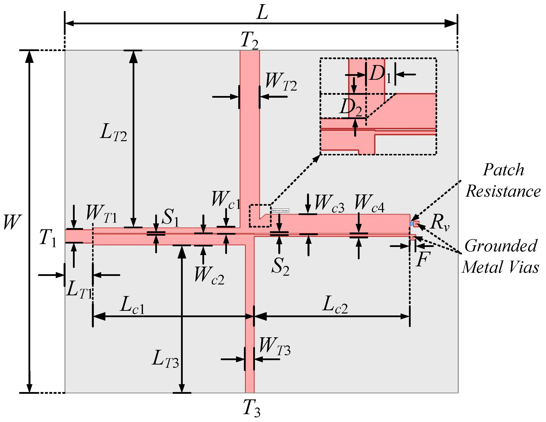
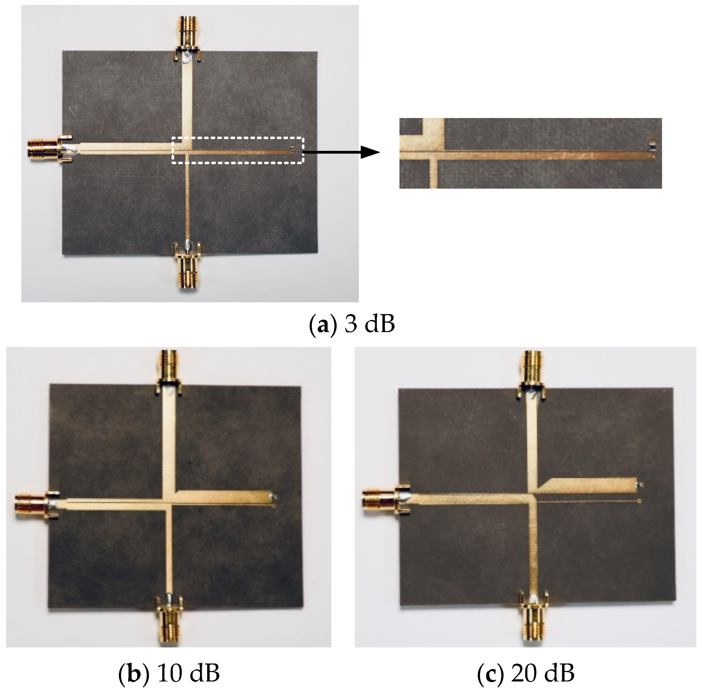
4.1. Design Processes and Circuit Fabrication

To verify the validity and accuracy of the proposed analysis and design approach for single-resistor ACPDs in Section 2.2, we fabricated three single-resistor ACPDs with different terminal real impedances and different PDRs (dB) of 3 dB, 10 dB, and 20 dB.
The targeted design parameter values of the three ACPDs are calculated and listed in Table 1, all of which are finally well satisfied. In the following, we use t to represent the coefficient t1. It should be noted that the values of x, y, t, K2, and K6 are arbitrarily selected for all ACPDs. Consequently, the value of the patch resistor is also specified artificially. The parameters of the substrate material are listed in Table 2. For the convenience of the test, two quarter-wavelength impedance transformers were introduced to the output ports T2 and T3 of ACPD to transform both terminal impedances ZT2 and ZT3 to 50 Ω. A 50 Ω transmission line with a fixed length of 5 mm was connected to the input port T1 to facilitate test connector connections.
The initial geometric parameter values of the three ACPDs, obtained by CLS, are listed in Table 3 (see Figure 8 for geometric parameter definitions). Subsequently, the parameters were fine-turned to further optimize the S-parameters. The fabricated geometric parameter values are listed in Table 4. It is evident that the initial values are highly accurate, as the difference between the initial values and the fabricated values is minimal. Pictures of the three fabricated ACPDs are shown in Figure 9a–c. It is noted that in Figure 9c, due to the large difference in the value of line spacing between the two ACL sections, the bottom line in the left ACL section is chamfered to facilitate connection.
Figure 8 shows geometric parameter definitions of the whole fabricated ACPD circuit. For the left ACL section, Wc1 and Wc2 are line widths, S1 is the line spacing, and Lc1 is the line length. For the right ACL section, Wc3 and Wc4 are line widths, S2 is the line spacing, and Lc2 is the line length. For the 50 Ω transmission line connected to T1, in the 3 dB, 10 dB, and 20 dB ACPDs, the width WT1 is equal to 2.4 mm, and the length LT1 is equal to 5 mm. For the quarter-wavelength impedance transformer connected to port T2, its width and length are defined as WT2 and LT2. For the one connected to port T3, its width and length are defined as WT3 and LT3. The small blue square on the right of Figure 7 represents the place for the patch resistor, whose package is 0402. The side length F of the ground square pad is equal to 1 mm. Two metal vias, with the radius Rv equal to 0.15 mm, are adopted to realize grounding.
It is noted that for the 10 dB and 20 dB ACPDs, we chamfered the upper line of the right ACL section. The chamfered part has been marked with the dashed box and its amplifying circuit is shown in the upper right corner of Figure 8, with two cutting distances, respectively, defined as D1 and D2. To visualize the effect of chamfering on device performance, Figure 10 shows comparison curves of the simulated S-parameters before and after chamfering, of the 20 dB ACPD. It is observed that chamfering mainly affects the resonant frequency of S22. Figure 11 gives the S22 curves under different values of D1 and D2. Clearly, with the increase of D1 and D2, the resonant frequency moves to the higher frequency. It can be inferred that when the value of Wc3 is large, the impedance transformer at T2 will produce a large coincidence area with the upper line of the ACL section on the right side, thereby increasing the electrical length of this ACL section, making the resonant frequency deviate from the central frequency to the lower frequency. Chamfering can reduce the electrical length to a certain extent, making the resonant frequency close to the central frequency.

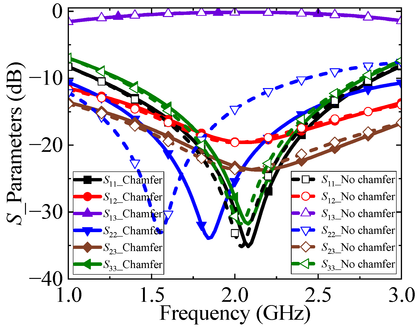
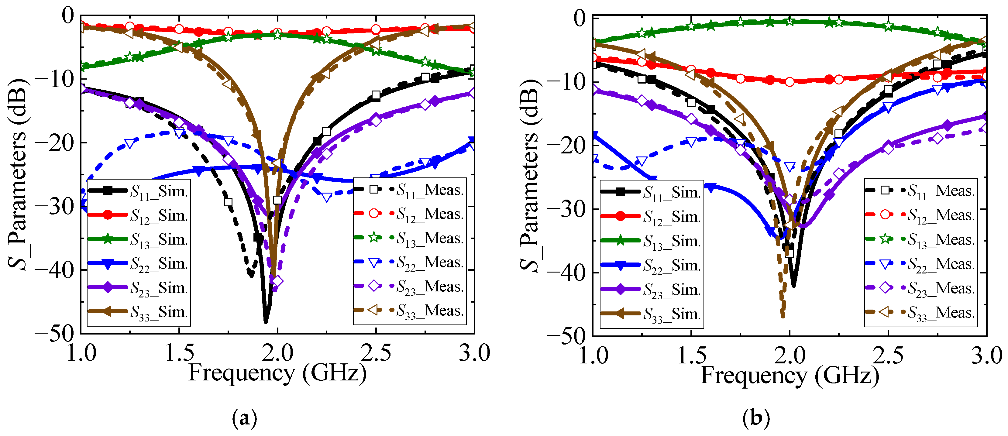
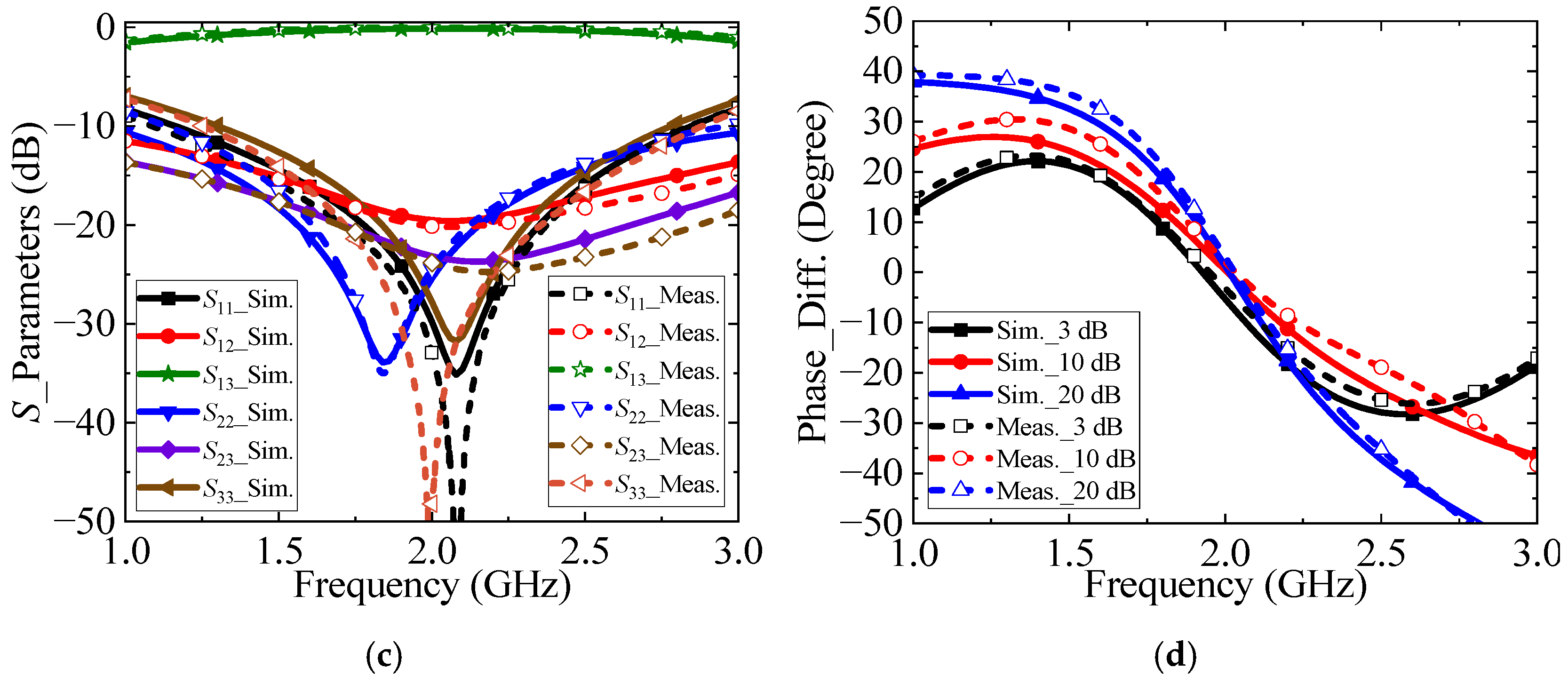
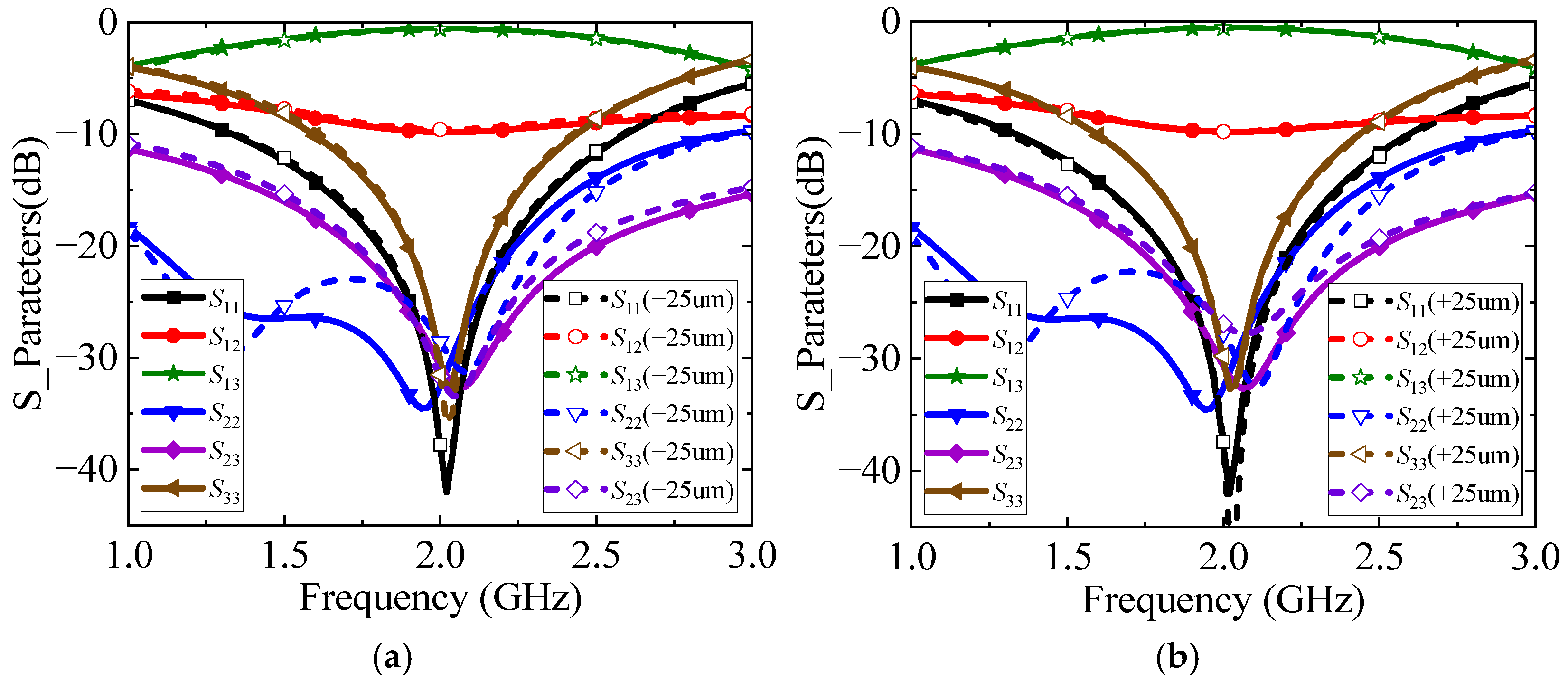
4.2. S-Parameter Performance Analysis

The observation frequency band is from 1 GHz to 3 GHz, with a central frequency of 2 GHz. Figure 12a–c present magnitude curves of the simulated and measured S-parameters of the above three ACPDs. Great consistency between the simulated and measured results is achieved. The 3 dB ACPD has a fractional bandwidth of 13% (1.84 GHz to 2.10 GHz). The 10 dB ACPD has a fractional bandwidth of 25% (1.74 GHz to 2.24 GHz). The 20 dB ACPD has a fractional bandwidth of 23% (1.84 GHz to 2.3 GHz). The definitions of S-parameter values for the fractional bandwidth calculation of the three ACPDs are listed in Table 5.
The frequency deviation of curves and differences between the simulated and measured results are related to objective errors such as fabrication inaccuracy, the effects of SMA connectors, substrate and conductor loss, layout discontinuity, board deformation, as well as the welding of patch resistors, to some extent. The line width and line spacing of PCB can be controlled in the order of 25 um. Figure 13 shows the simulated S-parameter curves of the 10 dB ACPD before and after changing the line spacing with the maximum fabrication error of 25 um. It is observed that the fabrication inaccuracy mainly influences S22 and nearly has no impact on the other S-parameters. It could be inferred that the inconsistency of S22 in Figure 12 is mainly caused by machining errors. In the operation frequency band, the insertion loss and reflection loss of SMA connectors can be controlled at a relatively low level (−0.1 dB, −20 dB). The values of the dielectric constant and dissipation factor of the material show little change.
Figure 12d shows the simulated and measured phase difference (PD) between the two output ports of three power dividers. The measured PDs at the central frequency (defined as PDC) are, respectively, equal to −3° (3 dB), 1.9° (10 dB), and 2.4° (20 dB), verifying the good in-phase characteristic. When the fractional bandwidth (FB) is defined as |PD − PDC| ≤ 10°, then the FBs of the three ACPDs are, respectively, equal to 17.5% (1.82 GHz to 2.17 GHz, 3 dB), 17.5% (1.84 GHz to 2.19 GHz, 10 dB), and 10.5% (1.9 GHz to 2.11 GHz, 20 dB). As the frequency deviates from the central frequency point, the PD increases gradually, which means the in-phase characteristics deteriorate. The reason for this phenomenon may be attributed to the increased difference between the c-mode and π-mode phase velocities, as the frequency deviates from the central frequency.

4.3. Performance Comparison

Table 6 presents the comparison results of the measured three ACPDs with other in-phase and out-of-phase power dividers. The comparison criteria include terminal real impedances, maximum achievable power division ratio, number of required isolation resistors, phase relationship of output ports, fractional bandwidth when isolation performance is better than −20 dB, type of circuit elements, and occupied area of main circuits.
Clearly, compared to other in-phase power dividers, our proposed ACPD features a simpler structure and smaller size. It also offers impedance transformation capability and achieves an exceptionally large power division ratio of 100:1, surpassing other power dividers in this aspect. Moreover, utilizing ACLs for the transmission path allows flexible placement of the two output ports, accommodating various application scenarios. It is worth noting that out-of-phase power dividers, commonly used in scenarios requiring out-of-phase outputs, typically achieve a large PDR easily. Therefore, their performance cannot be directly compared with that of in-phase power dividers.

5. Application of Devices with Arbitrary Terminal Real Impedances and Arbitrary Power Division Ratio

The design approach for arbitrary terminal real impedances and arbitrary power division ratio has wide application scenarios and significance importance. Although 50 Ω is a standard value for the characteristic impedance of coaxial transmission lines, the optimal input impedance for packaged antennas, amplifiers, and filters in RF integrated circuits is not necessarily 50 Ω. For conventional power dividers, all three terminals are typically matched to 50 Ω, requiring additional impedance transformers to achieve port match when connecting non-50 Ω devices. Additionally, different circuit systems have diverse input power requirements for terminal components connected to power dividers. The ACPDs we propose can simultaneously achieve impedance transformation, port match, and power dividing functions. This is beneficial to reduce circuit size and enhance the overall performance of the system.

6. Conclusions

For the first time, ACLs are introduced into the design of in-phase Gysel power dividers. By the simplified analysis of N-port networks and the decoupled branch-line model of ACLs, the design formulas are derived and provided in detail, for satisfying the perfect match and isolation simultaneously. From theoretical analysis, the limitations of the proposed ACPDs are pointed out. Moreover, to reduce the subsequent optimization iterations of devices, an automatic solution software is developed to obtain accurate initial values of ACL geometric parameters. For verification, three ACPDs with different PDRs of 1:1 (3 dB), 10:1 (10 dB), and 100:1 (20 dB) were implemented.
The proposed ACPD has several key advantages:
  • ACPD possesses the capability of flexible impedance transformation.
  • ACPD requires only one isolation resistor for both equal and unequal power division cases, and resistor values can be flexibly determined.
  • ACPD can easily achieve a large in-phase PDR. ACPD realized the large in-phase PDR of 100:1 (20 dB) and offers a broad in-phase PDR range from 1:1 (3 dB) to 100:1 (10 dB).
  • ACPD is compact and the positions of the two output ports can be arranged as needed.
The proposed approach in this paper for designing ACPDs offers enhanced design flexibility to RF engineers. It allows for specifying terminal real impedances, achieving any desired power division ratio, and placing the positions of the two output ports. These advancements significantly contribute to automating device design processes, thereby advancing the level of design intelligence in RF engineering.

Author Contributions

Methodology, validation, original draft preparation, Y.Z.; review and editing, B.X. and J.M. All authors have read and agreed to the published version of the manuscript.

Funding

This work was supported by the National Natural Science Foundation of China under Grant 62188102, Grant 92373112, Grant 62090015, Grant 92373201.

Data Availability Statement

Data is contained within the article.

Conflicts of Interest

The authors declare no conflicts of interest.

References

  1. Wincza, K.; Gruszczynski, S. Reduced-length tandem directional couplers composed of coupled-line sections with fixed coupling coefficient. IEEE Trans. Microw. Theory Tech. 2021, 69, 1625–1634. [Google Scholar] [CrossRef]
  2. Luo, Z.H.; Zhang, G.; Wang, H.W.; Li, N.; Tam, K.W.; Tang, L.M. Dual-band and triple-band filtering power dividers using coupled lines. IEEE Trans. Circuits Syst. II Express Briefs. 2023, 70, 1440–1444. [Google Scholar] [CrossRef]
  3. Li, D.; Xu, K.D. Multifunctional switchable filter using coupled-line structure. IEEE Microw. Compon. Lett. 2021, 31, 457–460. [Google Scholar] [CrossRef]
  4. Zhou, Z.; Ge, Y.; Yuan, J.; Xu, Z.; Chen, Z.D. Wideband MIMO antennas with enhanced isolation using coupled CPW transmission lines. IEEE Trans. Antennas Propag. 2023, 71, 1414–1423. [Google Scholar] [CrossRef]
  5. Zhou, R.; Chen, J.; Li, Z.; Yu, J.; Tang, D.; Hong, W. A 260-GHz power amplifier with 12.5-dBm Psat and 21.4-dB peak gain utilizing a modified coupled-line-balun network. IEEE Trans. Microw. Theory Tech. 2024, 72, 3031–3045. [Google Scholar]
  6. Tripathi, V.K. Asymmetric coupled transmission lines in an inhomogeneous medium. IEEE Trans. Microwave Theory Tech. 1975, 23, 734–739. [Google Scholar] [CrossRef]
  7. Zhang, Y.; Xia, B.; Mao, J.F. A design approach for asymmetric coupled line tandem couplers with arbitrary terminal real impedances and arbitrary power dividing ratio. IEEE Trans. Microw. Theory Tech. 2024, 72, 3542–3553. [Google Scholar] [CrossRef]
  8. Chen, H.; Zhou, Y.; Zhang, T.; Che, W.; Xue, Q. N-way Gysel power divider with arbitrary power-dividing ratio. IEEE Trans. Microw. Theory Tech. 2019, 67, 659–669. [Google Scholar] [CrossRef]
  9. Nemati, R.; Karimian, S.; Shahi, H.; Masoumi, N.; Safavi-Naeini, S. Multisection combined Gysel–Wilkinson power divider with arbitrary power division ratios. IEEE Trans. Microw. Theory Tech. 2021, 69, 1567–1578. [Google Scholar] [CrossRef]
  10. Chen, S.; Yu, Y.; Tang, M. Dual-band Gysel power divider with different power dividing ratios. IEEE Microw. Compon. Lett. 2019, 29, 462–464. [Google Scholar] [CrossRef]
  11. Lin, F.; Chu, Q.X.; Gong, Z.; Lin, Z. Compact broadband Gysel power divider with arbitrary power-dividing ratio using microstrip/ slotline phase inverter. IEEE Trans. Microwave Theory Tech. 2012, 60, 1226–1234. [Google Scholar]
  12. Ooi, B.L. Compact EBG in-phase hybrid-ring equal power divider. IEEE Trans. Microw. Theory Tech. 2005, 53, 2329–2334. [Google Scholar]
  13. Wang, X.; Wu, K.L.; Yin, W.Y. A compact Gysel power divider with unequal power-dividing ratio using one resistor. IEEE Trans. Microw. Theory Tech. 2014, 62, 1480–1486. [Google Scholar] [CrossRef]
  14. Wang, K.X.; Zhang, X.Y.; Hu, B.J. Gysel power divider with arbitrary power ratios and filtering responses using coupling structure. IEEE Trans. Microw. Theory Tech. 2014, 62, 431–440. [Google Scholar]
  15. Luo, M.; Xu, X.; Tang, X.H.; Zhang, Y.H. A compact balanced-to-balanced filtering Gysel power divider using λg/2 resonators and short-stub-loaded resonator. IEEE Microw. Compon. Lett. 2017, 27, 645–647. [Google Scholar]
  16. Gharehaghaji, H.S.; Shamsi, H. Design of unequal dual band Gysel power divider with isolation bandwidth improvement. IEEE Microw. Compon. Lett. 2017, 27, 138–140. [Google Scholar] [CrossRef]
  17. Zhang, Y.; Liu, P.C.; Xia, B.; Wei, G.R.; Xiong, C.; Mao, J.F. A new wideband RLGC extraction method for multiconductor transmission lines using improved mode tracking algorithm. IEEE Trans. Electromagn. Compat. 2024, 66, 293–301. [Google Scholar]
  18. Zhang, N.; Wang, X.; Zhu, L.; Lu, G. A novel unequal power divider with general isolation topology: Design and verification. IEEE Microw. Compon. Lett. 2023, 33, 19–22. [Google Scholar]
  19. Wu, Y.; Liu, Y.; Li, S. A modified Gysel power divider of arbitrary power ratio and real terminated impedances. IEEE Microw. Compon. Lett. 2011, 21, 601–603. [Google Scholar]
  20. Xia, B.; Cheng, J.D.; Xiong, C.; Xiao, H.; Wu, L.S.; Mao, J.F. A new Gysel out-of-phase power divider with arbitrary power dividing ratio based on analysis method of equivalence of N-port networks. IEEE Trans. Microw. Theory Tech. 2021, 69, 1343–1355. [Google Scholar] [CrossRef]
  21. Chiu, L.; Xue, Q. A parallel-strip ring power divider with high isolation and arbitrary power-dividing ratio. IEEE Trans. Microw. Theory Techn. 2007, 55, 2419–2426. [Google Scholar] [CrossRef]
Figure 1. Structure of the proposed ACPD with two isolation resistors, where Zci, Zπi, Zcir, and Zπir (i = 1, 2) are characteristic mode impedances of ACLs.
Symmetry 17 00562 g001
Figure 2. Decoupled circuit of the proposed ACPD at the central frequency.
Symmetry 17 00562 g002
Figure 3. Schematic of the 2-port subnetwork constituted by ports T2 and T3, where subcircuit A and B are isolation paths of resistors R1 and R2,respectively, and subcircuit C is the main transmission path.
Symmetry 17 00562 g003
Figure 4. Simplified circuit of the proposed ACPD at the central frequency for the power analysis.
Symmetry 17 00562 g004
Figure 5. Structure of the proposed ACPD with one isolation resistor, where Zci, Zπi, Zcir, and Zπir (i = 1, 2) are characteristic mode impedances of ACLs.
Symmetry 17 00562 g005
Figure 6. Flowchart of the processing steps of CLS.
Symmetry 17 00562 g006
Figure 7. The ACL model established by CLS in HFSS, with parameter definitions.
Symmetry 17 00562 g007
Figure 8. Geometric parameter definitions of the fabricated ACPD.
Symmetry 17 00562 g008
Figure 9. Pictures of the three fabricated ACPDs. (a) 3 dB. (b) 10 dB. (c) 20 dB.
Symmetry 17 00562 g009
Figure 10. Comparison curves of the simulated S-parameter magnitude before and after chamfering of the 20 dB ACPD.
Symmetry 17 00562 g010
Figure 11. Magnitude curves of S22 parameter under different values of (a) D1 and (b) D2.
Symmetry 17 00562 g011
Figure 12. Magnitudes of the simulated and measured S-parameters of (a) 3 dB ACPD, (b) 10 dB ACPD, and (c) 20 dB ACPD. (d) Simulated and measured phase difference between two output ports of the three ACPDs.
Symmetry 17 00562 g012aSymmetry 17 00562 g012b
Figure 13. Magnitudes of the simulated S-parameters of the 10 dB ACPD before and after changing the value of line spacing by (a) subtracting 25 um and (b) adding 25 um.
Symmetry 17 00562 g013
Table 1. Targeted parameter values of the three ACPDs.
ParametersxyRptK2K6K1K3K4K5
3 dB0.82.813310.88981.32292.19094.0988
10 dB0.61.70.10.723.61.51.49920.99100.68933.6693
20 dB0.861.260.010.633.4452.26950.81980.72198.7382
ParametersZT1 (Ω)ZT2 (Ω)ZT3 (Ω)R (Ω)ZI1 (Ω)ZI2 (Ω)ZI3 (Ω)ZI1r (Ω)ZI2r (Ω)ZI3r (Ω)
3 dB504014015044.4915066.145109.545204.9450
10 dB5030853674.9618049.5534.465183.46575
20 dB50436330113.47515040.9936.095436.91172.25
Table 2. Parameter values of the substrate material adopted.
ParametersL (mm)H (mm)T (mm)TanDεr
Values280.7870.0170.00092.2
Table 3. Initial geometric parameter values of the three ACPDs determined by CLS.
Parameters (mm)Wc1Wc2S1Wc3Wc4S2
3 dB2.140.890.150.160.870.15
10 dB1.041.880.153.350.370.21
20 dB0.162.410.143.790.241.98
Table 4. Geometric parameter values for fabrication of the three ACPDs.
Parameters (mm)Wc1Wc2Wc3Wc4S1S2Lc1Lc2WT1LT1
3 dB2.10.930.150.940.150.1529.4928.512.45
10 dB0.971.953.40.360.150.2128.6927.772.45
20 dB0.152.383.80.240.15229.6225.592.45
Parameters (mm)WT2LT2WT3LT3WLD1D2FRv
3 dB2.8325.12.427.0755.35700010.15
10 dB3.4631.732.426.4561.25702.82.4310.15
20 dB2.5226.752.425.2854.71704.723.6510.15
Table 5. Definitions of S-parameter values for the fractional bandwidth calculation of the three fabricated ACPDs.
S-ParametersS11/S22/S23/S33 (dB)S12 (dB)S13 (dB)
3 dB<−15−3 ± 0.2−3 ± 0.2
10 dB<−15−10 ± 0.5−0.4 ± 0.2
20 dB<−20−20 ± 1.5−0.03 ± 0.1
Table 6. Performance comparison of the fabricated three ACPDs with other power dividers.
Refs.TRIMPDRRNPhase
Relationship
FBW (%)Circuit Element TypeOccupied
Area (λg2)
[11]Fixed2:12In-phase137.5Branch lines with one slotline phase inverter as the isolation path0.072
[13]Fixed4:12/1 *In-phase57.69Branch lines with one SCL section as the isolation path0.114 1
[18]Fixed8:12In-phase66.67Branch lines with one coupled line section as the isolation path0.045
[19]Arbitrary2:12In-phase20.96Five sections of branch lines-
This
work
Arbitrary100:11In-phase34/42/60 2Two sections of ACLs0.033
[20]Arbitrary1000:11Out-of-phase100Branch lines with one SCL section as the transition path0.046
[21]Arbitrary12:12Out-of-phase120Parallel-strip ring with one swap as the isolation path-
ContributionImpedance transformation, miniaturization, high in-phase power division ratio
TRI, terminal real impedance; MPDR, the maximum achievable power division ratio; RN, number of the required isolation resistors; FBW, fractional bandwidth when isolation performance is better than −20 dB; *, only for unequal power dividing cases, one resistor is needed. For the equal power dividing case, two resistors are still required: 1, not directly provided in the paper. -, not presented in the paper; 2, 34, 42, and 60, respectively, correspond to the FBW of fabricated 3 dB, 10 dB, and 20 dB ACPDs proposed in this paper.
Disclaimer/Publisher’s Note: The statements, opinions and data contained in all publications are solely those of the individual author(s) and contributor(s) and not of MDPI and/or the editor(s). MDPI and/or the editor(s) disclaim responsibility for any injury to people or property resulting from any ideas, methods, instructions or products referred to in the content.

