Article

Assessment of the Technical Condition of High-Voltage Insulators during Operation

by
Dmitry Ivanov
*,
Aleksandr Golenishchev-Kutuzov
,
Marat Sadykov
,
Danil Yaroslavsky
and
Tatyana Galieva
Institute of Electricity and Electronics, Kazan State Power Engineering University, Kazan 420066, Russia
*
Author to whom correspondence should be addressed.
Machines 2022, 10(11), 1063; https://doi.org/10.3390/machines10111063
Submission received: 15 September 2022 / Revised: 31 October 2022 / Accepted: 9 November 2022 / Published: 11 November 2022
(This article belongs to the Special Issue Advances in Automation, Industrial and Power Engineering)

Abstract

:
During the operation process of high-voltage insulators, the characteristics of assessing their technical state are evaluated by using remote contactless monitoring and by subsequent forecasting of their residual life based on the developed set of diagnostic parameters of critical defects. Special attention is paid to the challenges of the practical application for remote contactless monitoring of high-voltage insulators’ current operating state. Measurements of characteristics for partial discharges on high-voltage insulators with various types of critical defects taken by electromagnetic and acoustic sensors are described. Based on the measurements, it was found that the unusual properties of the PD begin to manifest themselves starting from the intensities q ≥ 1.5–2 nC, and their maximum intensity can reach 5–7 nC. Up to PD intensities q ≤ 3 nC, most parameters of PD characteristics measured by electromagnetic and acoustic sensors correspond with an accuracy of 70–90%. It was found that for small defects with sizes d ≤ 300 μm in HVI, the PD intensity does not exceed 100 pC and depends little on the size of the defect. However, with an increase in the size of defects above 0.4–0.6 mm, a sharp rise in the intensity of the emerging VLPD begins.

1. Introduction

For more than 40 years, partial discharges (PDs) have been one of the main methods for monitoring the technical condition of high-voltage insulators (HVIs) during operation [1,2]. The main reason for the breakage of an HVI is the occurrence and further development of defects—mainly because of strong electric fields around the wires of high-voltage power lines. Therefore, the conditions for measuring a set of PD characteristics, to assess the HVI defects, are periodically improved, which is reflected in Russian and International standards. Moreover, at the beginning of the XXI century, it was theoretically predicted [3,4,5,6], and then experimentally established [7,8,9,10,11,12,13,14,15,16], that powerful PDs can also cause degradation of the HVI dielectric materials. However, the processes of PD generation under the action of high voltage are still poorly understood.
The study of physical processes accompanying PDs, which began at the end of the 20th century [1,2], received a new development after the discovery of very large partial discharges (VLPDs) at the beginning of the 21st century [3,4,5]. A VLPD is a PD in air insulators with an apparent charge value q ≥ 2.5 nC. Presently, there have been studies about several physical models of the formation of VLPDs and their influence on the degradation of dielectric elements of high-voltage power equipment. The main attention was paid to the new generation of polymer dielectrics, which have found wide application in capacitors, transformers, cables, and other high-voltage devices [6,7,8]. Less attention was paid to the experimental study of the appearance of VLPDs and their influence on the development of defects in actual high-voltage dielectric elements. In experimental studies, based on the results found in the available publications, the main attention was paid to defects in the forms of flat cavities or those filled with gas [9,10,11]. There are very limited studies of VLPDs in modern high-voltage insulators.
In the second decade of this century, this became the main reason to conduct a series of experimental studies on actual HVIs of electrical substations during their operation [17,18,19]. The main objectives were to study the dependencies of VLPD parameters on the characteristics of defects that cause them, as well as to develop methods for simultaneous noncontact detection of VLPDs by electromagnetic and acoustic methods [20,21,22,23]. The difficulty of this development of physical models of VLPD healing processes was that in actual HVI defects, unlike in model samples, there are more complex structural forms. Therefore, the main attention was paid to the most critical defects in the process of operation, such as ones in the forms of extended paths or cavities in the dielectric core rod and flat cavities at the interface “rod-end fitting”. These defects, as it was established during our experiments [12,13], are the main reasons for the appearance of VLPDs. Since many porcelain insulators are still currently being used in electrical substations, we conducted a comparative examination of the features of VLPDs in both types of HVI.

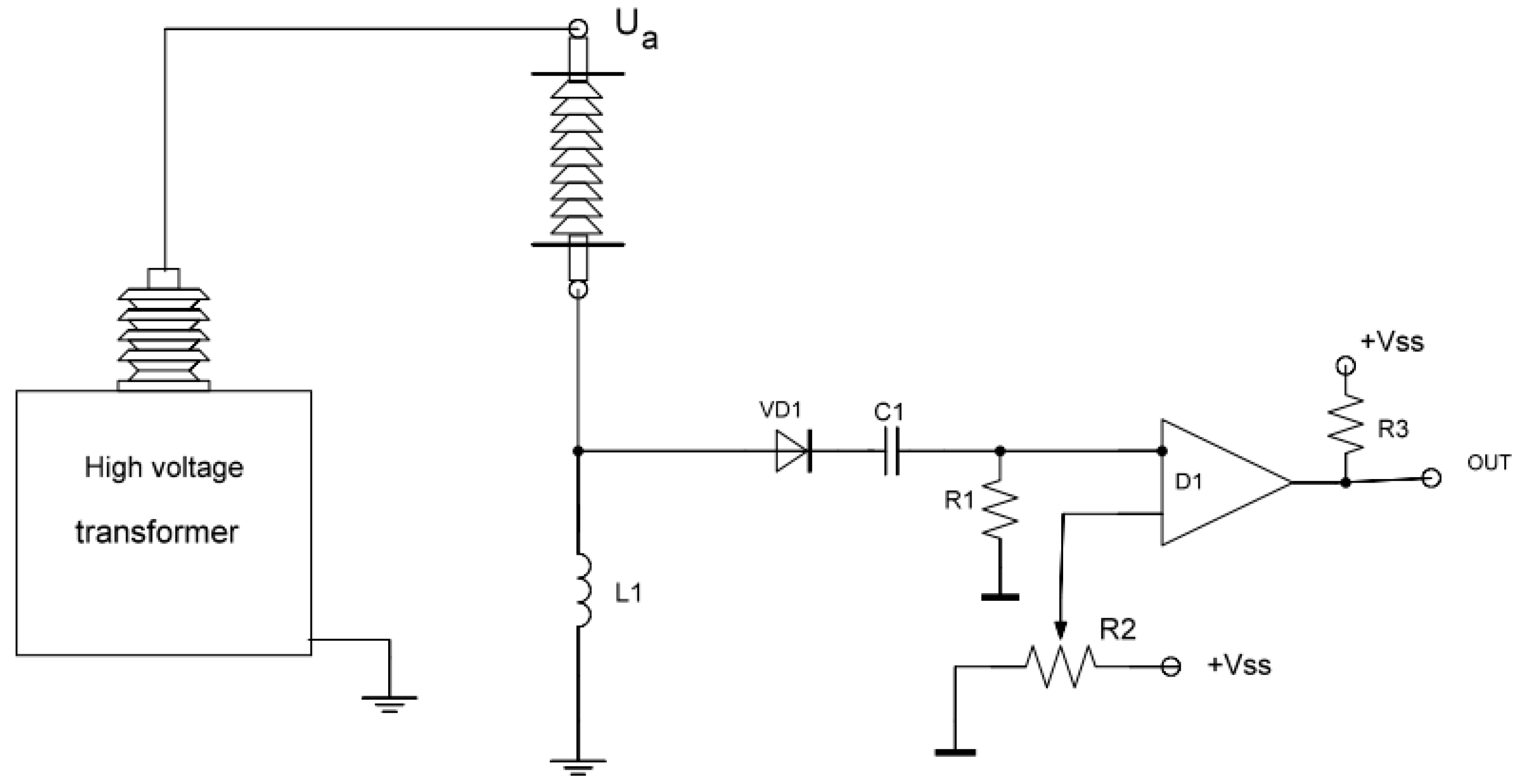
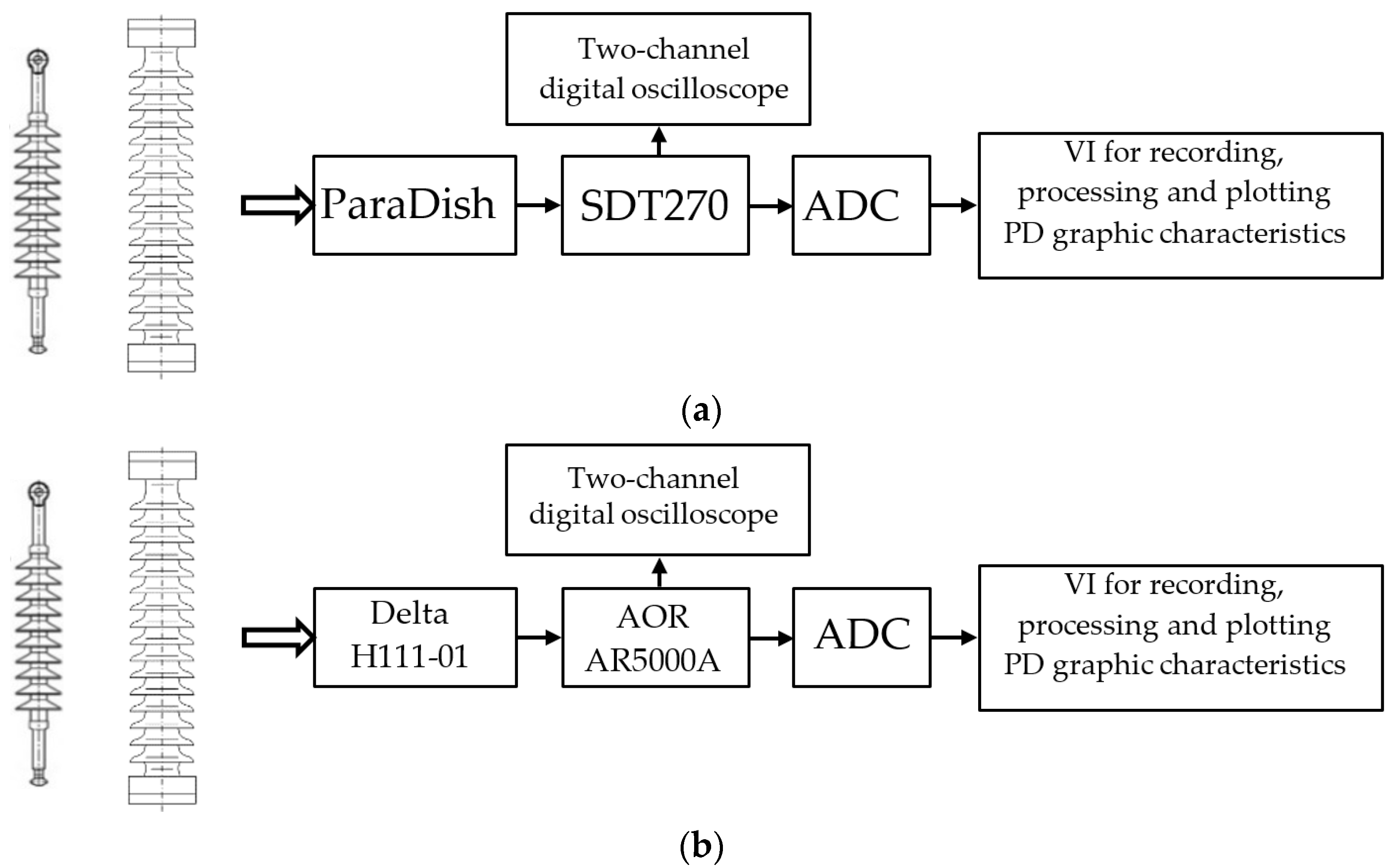
2. Materials and Methods

We started the first comprehensive research on the development of HVI technical condition monitoring on polymer (LK70/35) and porcelain (IOS 110/400) insulators. Laboratory tests were carried out on a test bench [24] by an electric (contact) method according to GOST R 55191-2012 (IEC 60270:2000) in combination with several contactless sensors for measuring PD parameters.
LK 70/35 linear suspension solid-cast polymer (organosilicon) insulators are designed for fastening and insulation of uninsulated and protected wires of 35 kV AC overhead lines with a frequency of up to 100 Hz at an ambient temperature of −60 to +50°C. IOS 110/400 insulators are designed for insulation and fastening of current-carrying parts in electrical apparatuses, complete switchgear, current ducts, switchgear of power stations and substations of alternating voltage over 1000 V, frequency up to 100 Hz.
At the first stage of the study by an electrical contact method based on GOST R 55191-2012 (IEC 60270:2000), the values of the apparent charge q of partial discharges were measured, and then the limit values q and the quantity of PD were set, characterizing the degree of defect for each type of polymer high-voltage insulators, simultaneously determined by visual inspection.
At the second stage, several methods of remote contactless monitoring of HVI technical condition parameters were developed, including various physical sensors [25], and a gradual transition from single sensors to the joint use of several sensors was assumed. Initially, a method was developed for the sequential study of HVIs on a test bench using electrical contact and contactless methods, and then two contactless methods to form the most effective complex method.
In accordance with GOST R 55191-2012 (IEC 60270:2000), an electric contact sensor was manufactured to register high-frequency current pulses induced in the grounding wire by PDs (Figure 1). A high-frequency filter is included in the grounding wire circuit to isolate the high-frequency component of the voltage, and it also acts as a measuring shunt. The peak detector is designed to isolate high-frequency PD pulses and generate a digital pulse recorded by the ADC board.
The calibration of the developed electrical contact sensor and the entire measuring system is performed using the CAL1B calibrator. With its help, short-term current pulses with a known charge value are introduced into the system, and thus a scale factor can be calculated for subsequent measurements of partial discharges.
In places of local defects, an electric charge arises, which can be discharged and emit pulses of alternating electric and magnetic fields into the surrounding space. The partial discharges occurring in the insulation cause current pulses in the grounding wire, which induce EMF induction in the inductor coil of the sensor. As a result, an electrical signal is removed from the sensor, which is directly proportional to the magnitude of the apparent charge of PD. This signal contains PD pulses and a sinusoidal component of the mains voltage [26,27].
The inductance of the filter reactor with an air core is used to isolate the high-frequency component of the voltage. At the same time, it acts as a measuring shunt; the peak detector is designed to isolate high-frequency PD pulses and generate a digital pulse recorded by the ADC board.
The inductance of the L1 filter is 20 mH. The capacitance of the capacitor C1 is 680 pF. The capacitance C1 generates a pulse with a duration of 100 microseconds, which is recorded using a peak detector. The peak detector is assembled according to the comparator circuit on the K554SA3 chip (IL311ANM analog).
PD is accompanied by the emission of short duration (from 10−11 to 10−7 sec.) electromagnetic pulses in a wide frequency range from 102 to 1010 Hz and acoustic pulses in the range of 20 Hz–500 kHz. For remote registration of such radiations, appropriate methods have been developed, each of which has both certain advantages and significant disadvantages. The electromagnetic method with high sensitivity is strongly influenced by radio frequency interference and electrical discharges from operating equipment on the accuracy of PD measurements; the acoustic method has high noise immunity from electromagnetic fields and good resolution to detect a defective insulator and in some cases even a defect site, which is combined with low sensitivity; optical and thermographic methods are effective only in the absence of solar illumination and work in a certain temperature range of the environment [28].
Taking into account the consideration of the peculiarities of the propagation of electromagnetic and acoustic waves, at present, even with the use of perfect directional antennas and amplifiers, it is impossible by these methods, as well as by using thermal imagers, to determine the locations and, moreover, the dimensions of defects remotely. There is only the possibility of locating single defective insulators within up to 100 m by an electromagnetic sensor, and the isolation of defective insulators within groups is possible only with the simultaneous use of electromagnetic and acoustic methods at shorter distances up to 10–15 m.
It follows from this that successful monitoring of the condition of insulating elements of high-voltage equipment is possible only with the simultaneous use of several methods discussed above. However, at present, almost all diagnostic devices manufactured by the industry are designed mainly for the use of one method, mainly either acoustic or thermographic, and have so far found application for monitoring the insulation of high-voltage power transformers and cables.
Since electromagnetic radiation of PD is a video pulse, various devices operating in the field of high or ultrahigh frequencies with a bandwidth of at least 15 kHz are used to measure the PD pulse signal, according to GOST R55191-2012 [29]. Registration of electromagnetic pulses PD (Figure 2) is carried out by an all-wave television antenna, “Delta N111-01”, with a gain of 28 dB, connected to a broadband tunable receiver, “AOR AR5000A”, which allows detecting signals in the frequency range of 0.5–800 MHz (Table 1). ADC is connected to the line output of the receiver. Registration of acoustic pulses is carried out by an active parabolic antenna, “ParaDish–2”, connected to a receiver, “SDT–270”, at a frequency of 40 kHz. The choice of measurement frequency was justified by such factors as the frequency dependence of wave attenuation, industrial noise and electromagnetic interference of the surrounding electrical equipment. Since acoustic noise dominates in the low-frequency region (20 Hz–20 kHz), the upper frequency limit is limited by the frequency dependence of attenuation (f ≥ 100 kHz). In the range of 35–45 kHz, as experiments have shown, with a signal-to-noise ratio of ≈2, acoustic pulses from PD are recorded at a distance of 10–20 m. Taking into account low-frequency industrial electromagnetic interference in the range of 50–200 MHz and above 600 MHz, the bands 20–50 MHz and 400–650 MHz are the most preferred for electromagnetic PD registration using our measuring complex, and the intensity of PD signals is significantly higher in the second band than in the first. Calibration was performed based on the results of the contact method (this method was used to calculate the intensity of PD (apparent charge)) and then by electromagnetic and acoustic methods.
Furthermore, the amplified signals from the receivers are displayed by a two-channel digital oscilloscope (DSO3062A) in the form of amplitude–time characteristics of PD pulses. Then the PD signals synchronized with the AC voltage phase of the network are sent to the ADC NI USB6341 (specifications are shown in Table 2) data acquisition board [30]. The digitized signals from the electromagnetic and acoustic receivers are fed into a computer in which, with the help of the developed program, information about the amplitude, repetition rate and phase of the signals is collected, recorded and processed (Figure 3). The accumulation of signals over narrow phase intervals (about 20°) occurs within 18 s, which fully satisfies the stochastic occurrence of PDs. The PD signal-processing process finishes with the construction of the following characteristics: the amplitude and number of pulses in each phase interval and the distribution of the number of pulses over the PD amplitudes.
The obtained phase distribution of pulse parameters is compared with the previously recorded distribution of pulse signal parameters for (defect-free) HVIs of the same type.
The determination of the real value of the intensity of a separate partial discharge is performed after calibration of the receivers of electromagnetic and acoustic signals using a contact sensor according to the method given in GOST R 55191-2012, taking into account the distance between the antenna and the PD source measured by a laser rangefinder.
The process of recording the initial array of PD characteristics is performed in the internal memory of the device, and then the initial data array is formed. After processing the initial array, the PD characteristics are displayed by a virtual data processing device (Figure 3). The structural diagram of the system is shown in Figure 2.
To receive signals from sensors and process and present the result in the form of graphical diagrams, as well as record measurement results as a file in computer memory, the LabVIEW 14.0 virtual instrument development environment is used as the most convenient tool for programming the three main components of the experiment: collection, analysis and presentation of the result.
In the diagram block, the number of PDs is determined for every twenty phase degrees of the mains voltage period. In the phase diagrams, after software processing, each PD corresponds to a point corresponding to the phase of occurrence of the PD and the amplitude depending on the power of the PD.
On the PD distribution graph, all single points form clusters of points with a close amplitude and phase of occurrence. In the same way, the dependence of the amount of PD on the amplitude is constructed and the average amount of PD is found in each phase interval.
For comparative analysis, normalized PD distribution graphs are constructed using the developed program, where the height of the columns depends on the number of PDs for a certain phase interval of the mains voltage. The phase interval with the largest number of recorded PD pulses is taken as the maximum, and relative to it, as a percentage of the maximum value, the height of the columns characterizing the relative number of PDs in other phase intervals is determined. At the end of plotting, the measurement results are saved in a file.

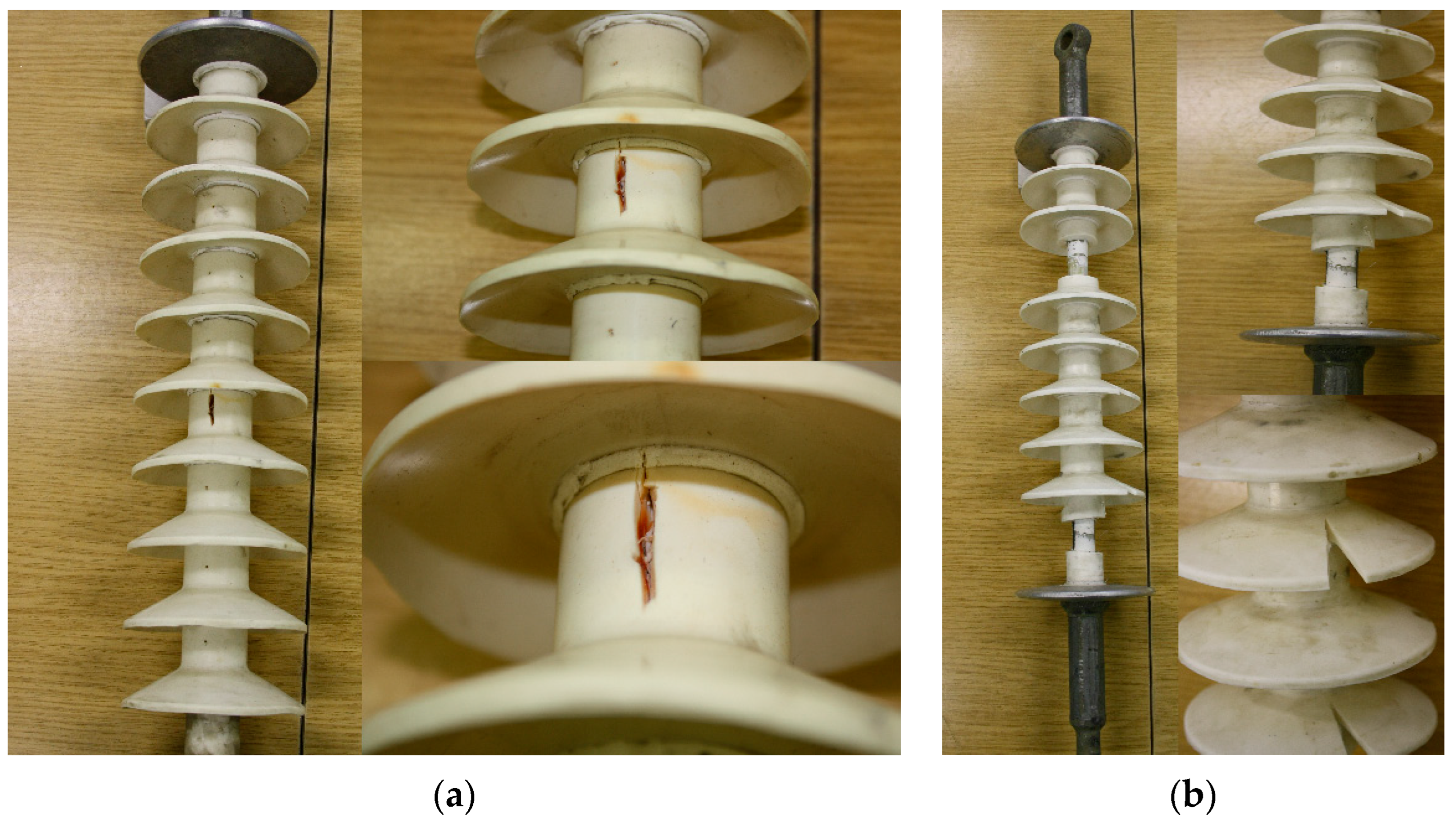
3. Results and Discussion

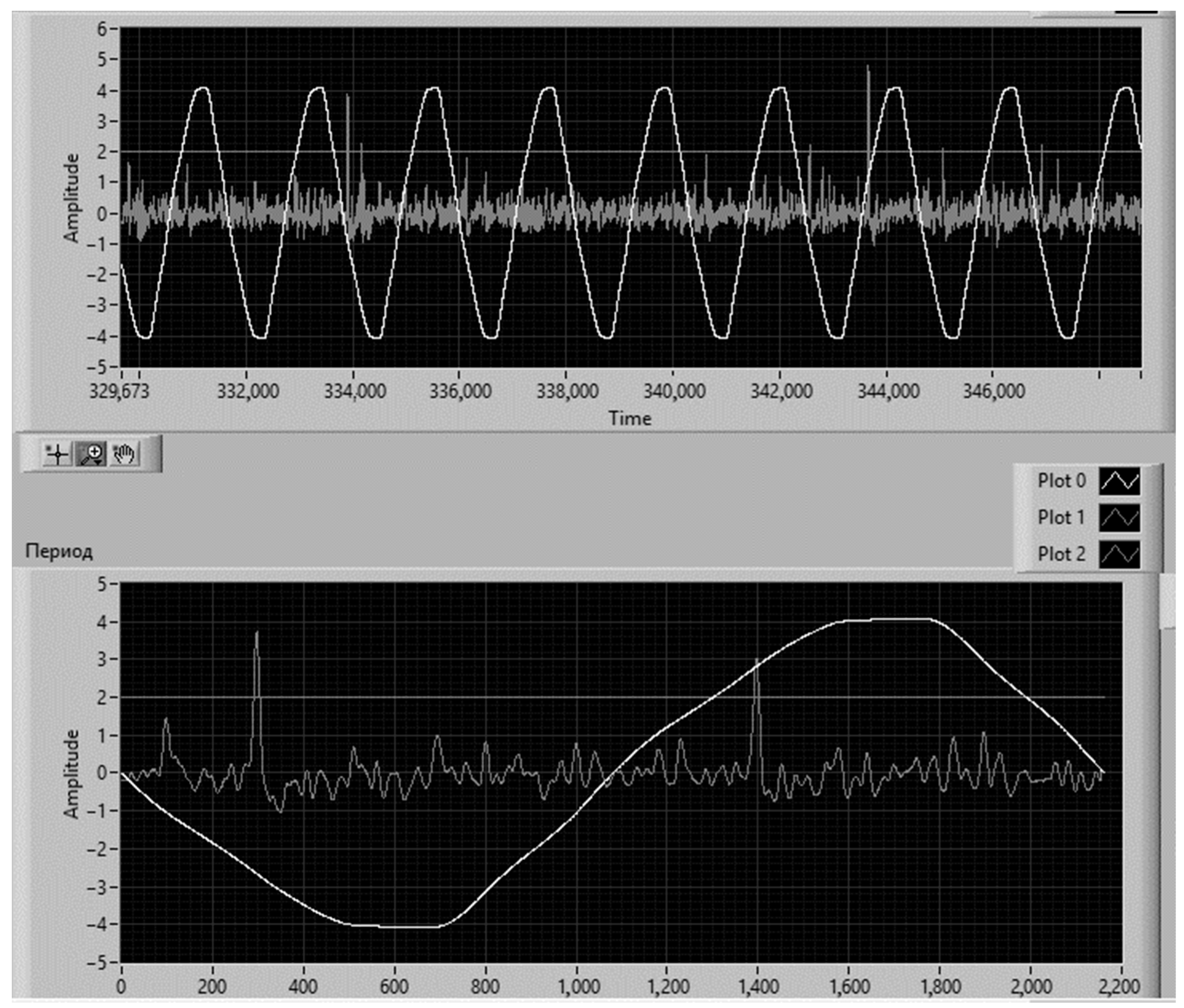
3.1. Measurement of Parameters of Very Large Partial Discharges

By using noncontact electromagnetic and acoustic sensors, the PD and VLPD characteristics were obtained at the stand of the PES department of the KSPEU and at several substations of JSC “Grid Company” in polymer (LK70/35, Figure 4) and porcelain (IOS 110/400) insulators.
Based on the measurements, it was found that the unusual properties of PD begin to manifest themselves as early as at intensities q ≥ 1.5–2 nC, and their maximum intensity can reach 5–7 nC. Moreover, up to PD intensities q ≤ 3 nC, most of the parameters of PD characteristics measured by electromagnetic and acoustic sensors coincide with an accuracy of 70–90%, except for the absolute values of the intensity q and the amount N.
Considering the above findings, we divided the sets of PD parameters in the study samples into three groups (Table 3): with intensity of 1.5 nC (1), 1.5–2.5 nC (2) and above 3 nC (3). We divided the sets of PD parameters in the studied samples into three groups: (1) fully serviceable HVIs, (2) operable HVIs with defects and (3) emergency HVIs with the need to be replaced during scheduled repairs.
This division is clear, since the influence of the induced charges of the previous PDs on the formation of VLPDs arises starting with just the second group, and development of differences in the detected PD signals by electromagnetic and acoustic sensors begins. The most significant differences between the sets of parameters PD and VLPD, given in Table 1, which, in our opinion, could serve as the basis for the development of a system of diagnostic parameters for assessing the technical condition of HVIs during operation, include the following:
-
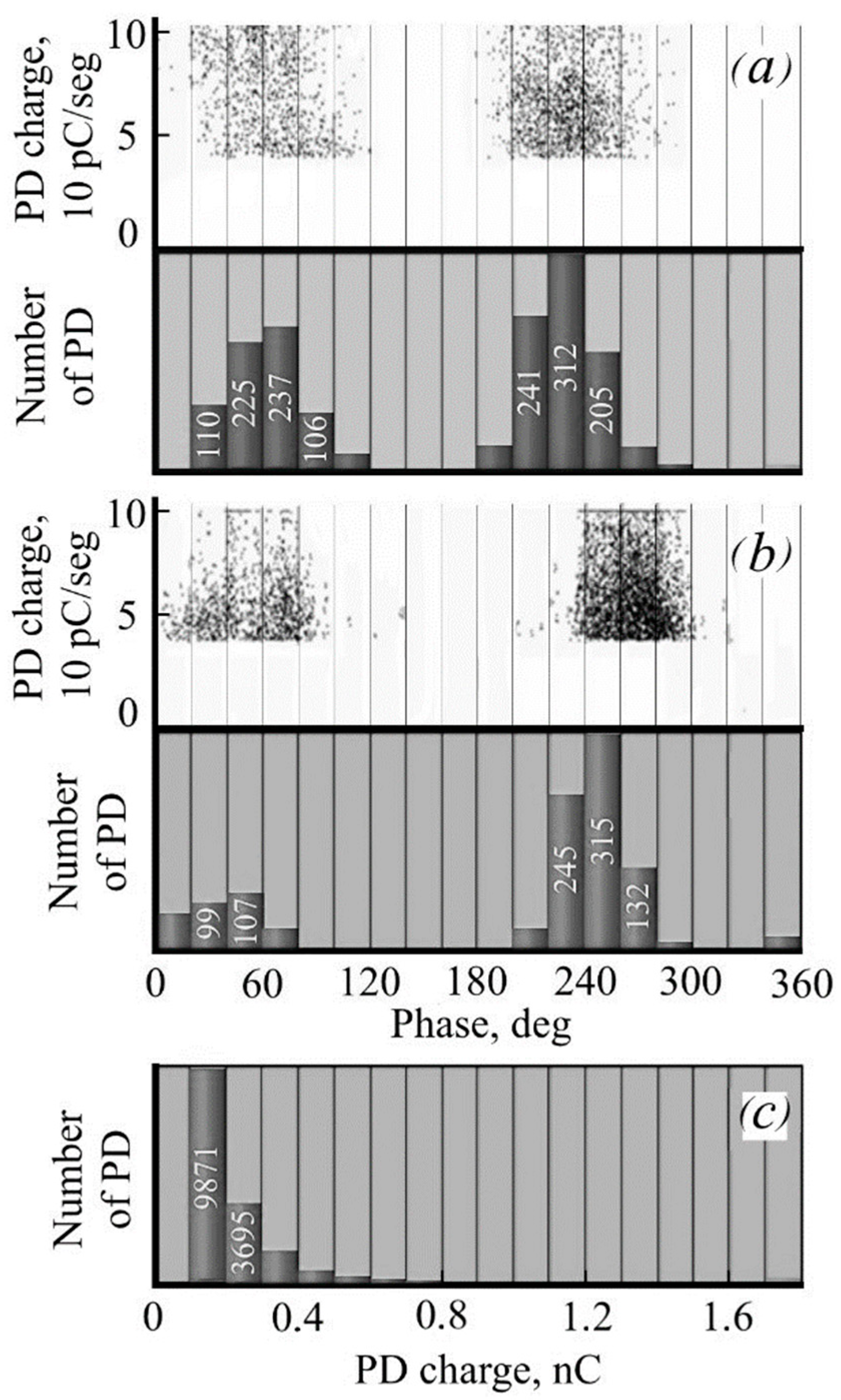
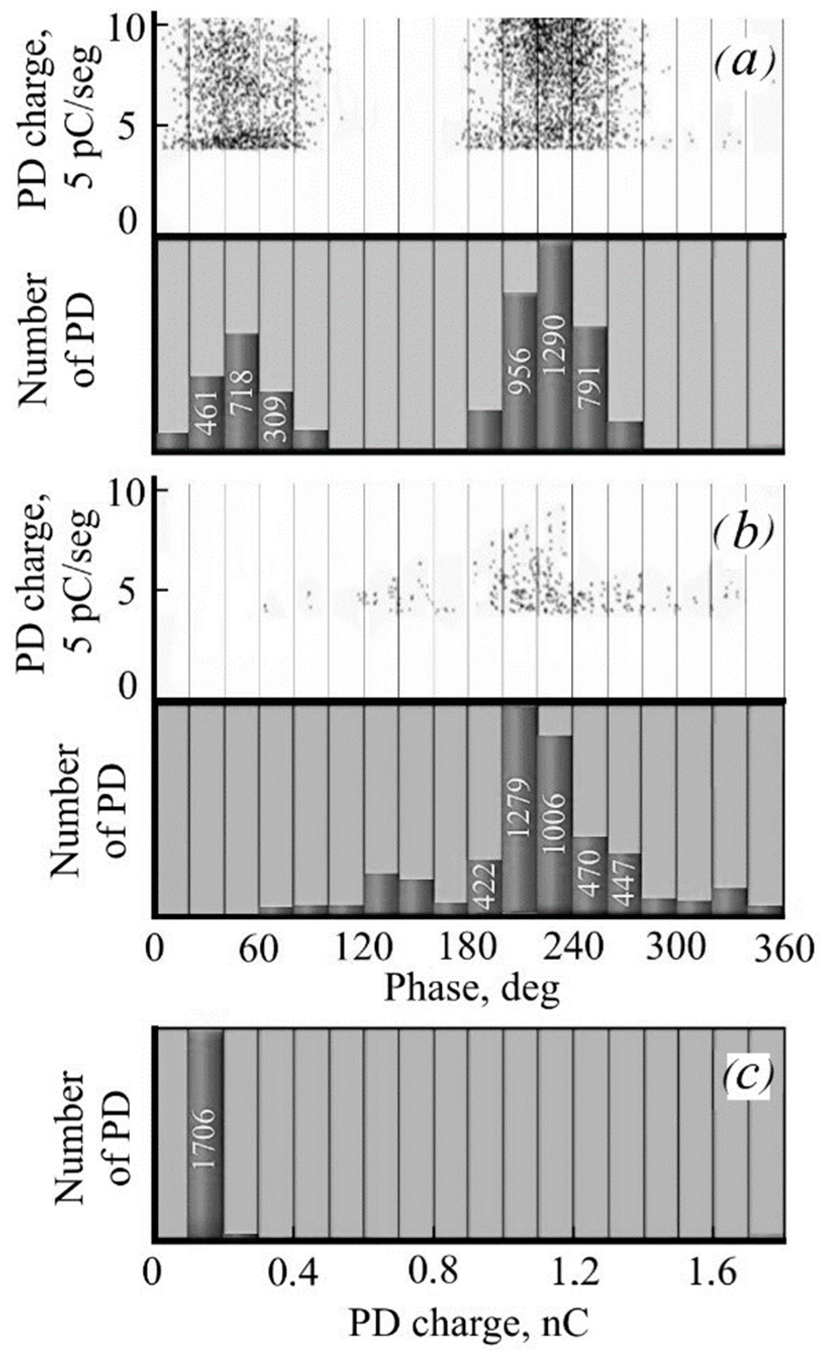
Occurrence of a VLPD near zero values of the applied high voltage Ua (that is, at phases 0°-180°-360°), Figure 5;
-
Increase in the number of VLPDs in negative Ua half-periods in relation to positive half-periods. If for the first two groups of samples this ratio N+/N− is close to unity, then for the third group N−/N+ ˃ 1, and it increases with increasing defectiveness;
-
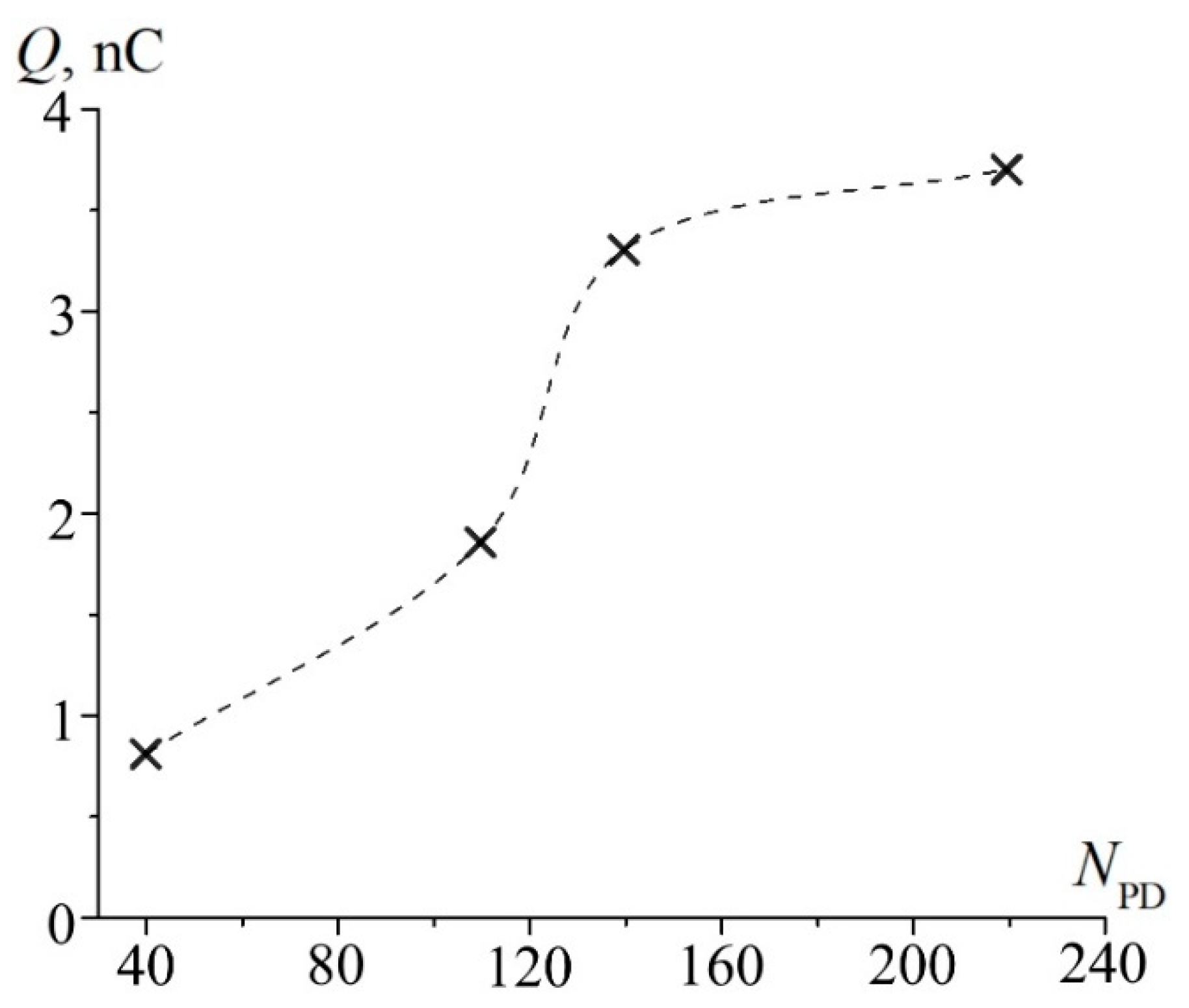
An increase in the number of VLPDs and a simultaneous decrease in the total number of PDs with an increase in the size of defects (Figure 6);
-
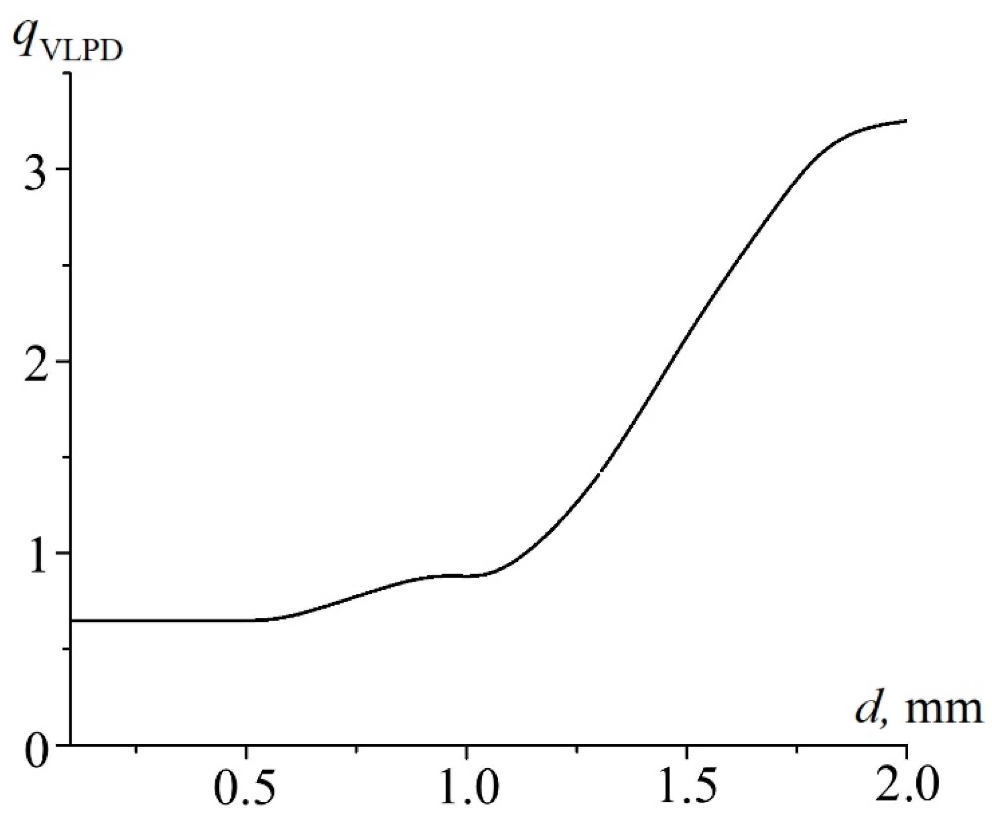
An increase in the VLPD intensity with an increase in the size of defects (Figure 7).
It should be noted that the above features of the characteristics of PDs and VLPDs were also discovered and discussed during the studies of defects in the forms of spheres or elongated three-dimensional ellipsoids in samples of polymer materials in Great Britain [10], China [11], and the USA [16]. Presented below is a comparison of the results of several VLPD parameters [12] with the parameters of defects in actual HVIs from our research with the results obtained on model samples.
It was found that for small defects (d ≤ 300 μm) in HVIs, the PD intensity does not exceed 100 pC (Table 3) and has low dependency on d. However, with an increase in the size of defects above 0.4–0.6 mm, a sharp rise in the intensity of the emerging VLPD begins.
The amount of VLPDs (q ≥ 2 nC) significantly increases with an increase in the size of the defect (Table 4, Figure 6), and then, at d ≤ 2 mm, the increase in the amount of VLPDs nearly stops (Figure 7). This sharp change in the intensity and amount of VLPDs is most typical for “rod-end fitting” defects. It is quite consistent with the dependence of the VLPD intensity on the radius of a spherical cavity in a dielectric given in [4,16]. However, only some physical processes related to the q (d) dependence for spherical defects are presented there.

3.2. Characteristics of Partial Discharges in High-Voltage Insulators

Since it was not possible to find a consideration of the PD features in actual HVIs in the available publications, and in view of several discovered features and differences in the PDs, and especially VLPDs, parameters measured simultaneously by two methods, an attempt was made to discuss the physical processes of generation of various types of PD in HVIs in more detail.
Partial discharge by definition [2] refers to the pre-breakdown stage of a spark discharge and represents the emergence and rapid development of a thin plasma channel in the gas gap between two electrodes with a high intensity of charged particles—electrons and positive and negative ions. In essence, PD has a streamer character and propagates along the gas cavity at a speed of 106–107 m/s, which exceeds the speed of propagation of electrons in free space under the influence of electric fields. The difference in the velocities of propagation of streamers formed by electrons and ions leads to spreading of the flow and expansion of its area. This circumstance can lead to an increase in its charge, which creates an induced electric field on the dielectric surfaces of the defect. The propagation of a charge streamer is accompanied by the emission of pulses of electromagnetic waves in the frequency range 107–1011 Hz. According to modern concepts [1], a space charge wave arising in the free space of a cavity with an increase in the field strength can be viewed as a transformation of the primary streamer in the defect area into a partial discharge. The latter, by definition, is the result of an increase in the applied field strength in the defect area, which exceeds the electrical strength of HVI at this location.
The streamer theory of electrical breakdown of gases [1] also allows for an explanation of the appearance of pulses of acoustic vibrations accompanying PD. This process occurs due to a sharp increase in the area of the streamer conducting channel in the discharge gap, at which the pressure at the boundaries of the streamer increases with the appearance of shock waves. In turn, the aggregate of shock waves generates pulses of acoustic waves detected by piezoelectric sensors. Experiments have shown [31] that PD pulses detected by acoustic sensors with a resonance frequency of 150 kHz have a rapidly growing leading edge with a duration of ~15–20 ns and a smoothly falling edge (Δt ~ 100 μs). It can be assumed that the duration of the leading edge is determined by the time of the pressure jump in the head of the streamer and does not depend on the conditions for the accumulation of charges on the dielectric surfaces of the defect. As follows from the VLPD characteristics measured by electromagnetic and acoustic sensors (Figure 8), acoustic measurements allow obtaining more accurate data on the parameters of defects than electromagnetic measurements, especially for extra-large defects. The reason for this fact is that acoustic measurements occur mainly during the period when the streamer passes the gas gap in the defect, and electromagnetic measurements include the propagation of the PD pulse along the dielectric surface of the defect. In samples with relatively small defects, the influence of the field’s ES induced by previous PDs on dielectric surfaces on the total field in the defect is insignificant, and the phase distribution of the intensity and amount of PD is determined by the strength of the applied field in the region of the defect fEa. Therefore, the PD characteristics in such samples (Figure 5), measured by electromagnetic and acoustic sensors, are similar in their parameters.
With an increase in the size of the defect (the third group of samples), the influence of the induced field’s ES, induced by the previous PDs on the dielectric surfaces of the defect, increases, and the total field Ed inside the cavity of the defect is represented as a geometric sum of the field strengths.
Ed = f Ea + ES,
where Ea is the strength of the field applied to the electrodes of the voltage, f is the factor of the change in the strength of the applied field, which depends on the geometry of the defect cavity and the ratio of the dielectric constants of the gas and the dielectric core-rod.
This effect is most pronounced in the defect between the core-rod and the end fitting of the insulator. At PD, a discharge first occurs with the propagation of a streamer in the cavity parallel to the applied field, and then it is replaced by a discharge along the dielectric surface perpendicular to Ea. In the latter case, the normal component Ea presses the drifting charges to the dielectric surface, which leads to an increase in the temperature and conductivity of the surface discharge channel. In this case, the intensity of the VLPD, as well as the width and number of VLPD pulses, will increase or decrease at certain phases of the applied voltage.
Thus, it can be assumed that the use of acoustic PD detection in defect control makes it possible to more accurately determine the total number of PDs, including VLPDs, and their phase distribution, while electromagnetic detection can successfully estimate the intensity and number of VLPDs, and, consequently, the type and size of large defects. These circumstances indicate the need to use both methods of PD detection for a more complete examination of the HVI operability during operation.

3.3. Generalized Physical Model of Very Large Partial Discharges

To date, only a few physical models have been developed that can describe the propagation of streamers in gas layers of defects in the forms of spheres or three-dimensional ellipsoids [16]. They are based on the proposed dependence of the intensity q of VLPDs on the total surface of the defect cavity [1]
q = π ε0 ε b2 [1+εr (K (a/b) − 1)] EPD,
where ε0 and εr are the dielectric constants of the gas and the dielectric respectively; a and b—longitudinal and transverse dimensions of the defect cavity; the values of the K-factor of inverse polarization were empirically determined in [10]: K ≈ 1 (a/b ˂˂ 1), K = 3 (a/b ~ 1), K ≈ 4 a/b (1 ˂ a/b ˂ 0).
This demonstration was used in [5,11] when studying the features of PD in model polymer samples. However, in these studies, little attention was paid to such simultaneous processes in the gas gap as an increase in the streamer propagation velocity with an increase in the length of the discharge gap with a corresponding increase in the field strength in the cavity ES and a simultaneous decrease in the field strength fEa applied to the cavity. However, it was previously suggested [1] that this effect can be empirically represented in the form
Ud = B dn,
where coefficient B determines the dependence of the breakdown voltage on the size of the discharge gap d and the gas pressure in the defect cavity. In this approximation, for small d ≤ 1 mm, the coefficient n approaches 1, and for large d ˃ 1 mm, the value of n decreases to 0.5–0.7. The proposed dependence was found for samples of the first and partially of the second group and in model samples [16]. Moreover, in both experiments, a significant change in the q(d) dependence was observed near d ≈ 1 mm.
Earlier, less attention was paid to the characteristics of PD propagation at the second stage along the dielectric surface of the defect. The above-mentioned studies did not consider the distribution of the charge density on the dielectric surface and their change during the period of the applied voltage. Processes of PD propagation through a cavity in a dielectric bounded by one electrode with one side were analyzed in [3,5,12]. In these works, it was shown that an increase in the area of the pulse propagation channel on the surface of the dielectric leads to a delay in its decay and a change in the total power. Apparently, this circumstance is the main reason for the discrepancy between the results on the number, intensity, and phase distribution of VLPDs obtained using electromagnetic and acoustic sensors.
Another discrepancy in the characteristics of VLPD generation for plane-shaped defects, studied in actual HVIs, and spherical-shaped defects, studied in several foreign studies [10,16], is that in spherical defects, PD relaxation occurs through the interaction of electrons and ions from two opposite segments of the surfaces of the defect sphere. The highest VLPD intensity is achieved when the radius of the sphere increases, and the field strength coincides with the intensity of the applied voltage by 8 times, the maximum charge VLPD by 13 times with a simultaneous decrease in the total amount of PD also over a period of 2.6 times with an increase in the radius of the sphere from 0.55 to 1.175 mm [4].
In actual HVIs, the relaxation of VLPD charges is carried out by their scattering on dielectric surfaces of defects. Therefore, an increase or decrease in the VLPD charge will largely depend on the distribution of the induced charge on the surface, which itself is determined by parameters such as surface conductivity and dimensions. These parameters have a contradictory effect on the surface-induced field ES. An increase in conductivity leads to an increase in the rate of movement of charges along the surface and an increase in the area of charges on the surface. This effect, as shown in [3], creates an increase in surface charges and an increase in the VLPD intensity. It is most typical for the propagation of streamers formed by positive ions, as was shown on model samples [3,4] and on actual HVIs. The broadening of the positive PD pulse shape in the falling part is associated with the expansion of the streamer area on the surface. In this case, no such broadening of negative PD pulses was observed.
It is necessary to emphasize the peculiarities of the difference in the phase intervals of VLPD generation for defects on the core and the “rod-end fitting” contact. In the first case, the accumulation of induced PD and VLPD occurs alternately on both boundary surfaces of the defect. In the second case, it occurs only at one dielectric end of the cavity, since the second end is a metal electrode. This feature is reflected in the phase distribution of the VLPD.
In a certain simplification, according to the above demonstration (2) for the dependence of the PD intensity on the shape of the cavity in the form of an ellipsoid, the first type of defect can be attributed to the type a ˃ b, and the “rod-end fitting” defect to the form a ˂ b. This assumption has already found experimental confirmation [13]
Ēn = Ēa + Ēs

4. Conclusions

The performed analysis of the parameters of VLPD characteristics showed that a possible set of diagnostic parameters of the HVI operating state can be based on several phase-dependent characteristics of very large partial discharges, because they are one of the main sources of accelerated development of defects. Specifically, in the primary control of HVI defectiveness, such diagnostic parameters can be the values of the coefficients of the ratio of the number of VLPDs to the total number of PDs for a certain measurement interval and the coefficient of the ratio of the number of PDs in the positive and negative half-periods of the applied high voltage.
The difference in the process of passage of the PD pulse through the gas cavity and then through the dielectric surface of the defect can be explained as follows. At the first stage, PD in the form of a streamer propagates along the applied electric field and consists of free electrons, as well as positive and negative ions. At the second stage, PD can propagate to the entire plane of the dielectric rod of the insulator, whereas at the first stage, the streamer occupies only a part of the cross section of the gas cavity. However, an increase in the defect cavity size, leading to an increase in the streamer propagation velocity and the number of induced electrons, also increases the very large PD intensity.
Since the speed of electrons is an order of magnitude higher than the speed of ions, the streamers consist mainly of electrons. At the second stage, the flow of charged particles in PD passes to the dielectric surface of the defect and can significantly expand within the entire surface of the defect. At this stage, there are residual charges formed by positive and negative ions. By increasing the PD intensity on the surface, additional optical radiation appears in the ultraviolet region until the moment of recombination of positive and negative ions on the dielectric surface.
A significant increase in the PD intensity in the negative part of each period of applied voltage is caused, in our opinion, by several factors: an increase in the area of the PD itself on the dielectric surface, the accumulation of charges from previous PDs and an increase in surface conductivity. It is their combination that creates stochasticity in the parameters of the PD sequence. Especially important in such a process is the occurrence of powerful PDs (q ≥ 5–10 nC) when adding in the phase range (180–240º) the applied and induced field strengths of the previous PDs.
An increase in the intensity and amount of PD detected by an acoustic sensor, with a simultaneous decrease in the same PD parameters detected by an electromagnetic sensor, is caused, in our opinion, by a change in the process of generating acoustic waves under the conditions considered above. In the second case, when such an electromagnetic pulse propagates along the dielectric surface, due to acoustoelectronic interaction, acoustic waves arise with an intensity proportional to the drift velocity of charge carriers υd. In such a process, the electronic amplification factor of ultrasound γe is proportional to the velocity ratio
γe = αeds − 1),
where αe is the electron acoustic absorption coefficient in the absence of charge carrier drift and υs is the speed of sound.
Since in this case the velocity υd significantly exceeds υs, as indicated in [32], significant acoustic wave intensities can be generated.
The gradual increase of these very large PDs seems to be the main reason for the accelerated aging of the insulation in high voltage power systems. Since such powerful PDs occur no more than once per period of applied high voltage, their detection was practically impossible using averaged recording methods due to the stochastic nature of their characteristics.
This circumstance creates a difference in the intensity of PDs detected by electromagnetic (channel PD) and acoustic (planar PD) sensors. This conclusion is confirmed by theoretical calculations performed on model samples of defects [19].

5. Patents

  • Certificate of state registration of the computer program No. 2021668517 Russian Federation. Software package for recording and processing partial discharge signals in the process of monitoring the technical condition of high-voltage insulators: publ. 17 November 2021/D. A. Ivanov, A.V. Golenishchev-Kutuzov, A.V. Semenikov, T. G. Galieva; applicant Federal State Budgetary Educational Institution of Higher Education “Kazan State Energy University”;
  • Utility model patent No. 206382 U1 Russian Federation, IPC H02J 13/00. Device for operational monitoring of the technical condition of high-voltage power transmission lines: No. 2021113356: application 11.05.2021: publ. 8 September 2021/M. F. Sadykov, M. P. Goryachev, D. A. Yaroslavsky [et al.]; applicant Federal State Budgetary Educational Institution of Higher Education “Kazan State Energy University”;
  • Certificate of state registration of the computer program No. 2022662455 Russian Federation. A program for processing signals from acoustic sensors: publ. 17 November 2021/Ivanov D.A., Galieva T.G., Sadykov M.F., Yaroslavsky D.A., Goryachev M.P., Khamidullin I.N., Vagapov A.I.; applicant Federal State Budgetary Educational Institution of Higher Education “Kazan State Energy University”.

Author Contributions

Conceptualization, D.I., A.G.-K. and M.S.; methodology, D.I., D.Y. and A.G.-K.; software, M.S. and D.Y.; validation, T.G. and M.S.; formal analysis, T.G. and D.Y.; investigation, D.I. and A.G.-K.; data curation, A.G.-K. and D.I.; writing—original draft preparation, D.I.; writing—review and editing, A.G.-K. and D.Y.; visualization, D.I.; supervision, A.G.-K.; project administration, M.S.; funding acquisition, D.I. and M.S. All authors have read and agreed to the published version of the manuscript.

Funding

The research work was carried out under the financial support of the Ministry of Science and Higher Education within the scope of the state Research and Development task no. 075-03-2022-151 of 14 January 2022 “Distributed automated systems of monitoring and diagnostics for technical condition of overhead power lines and substations based on broadband data transmission technology through power lines and the industrial Internet of Things”.

Conflicts of Interest

The authors declare no conflict of interest. The funders had no role in the design of the study; in the collection, analyses, or interpretation of data; in the writing of the manuscript or in the decision to publish the results.

References

  1. Niemeyer, L. A generalized approach to partial discharge modeling. IEEE Trans. Dielectr. Electr. Insul. 1995, 2, 510–528. [Google Scholar] [CrossRef] [Green Version]
  2. Vdoviko, V.P. Chastichnye Razryady v Diagnostirovanii Vysokovol’tnogo Oborudovaniya (Partial Discharge in the Diagnosis of High-Voltage Equipment); Science: Novosibirsk, Russia, 2007; p. 150. [Google Scholar]
  3. Pan, C.; Meng, Y.; Wu, K.; Han, Z.; Qin, K.; Cheng, Y. Simulation of partial discharge sequences using fluid equations. J. Phys. D Appl. Phys. 2011, 44, 255201. [Google Scholar] [CrossRef]
  4. Illias, H.A.; Chen, G.; Lewin, P.L. The influence of spherical cavity surface charge distribution on the sequence of partial discharge events. J. Phys. D Appl. Phys. 2011, 44, 245202. [Google Scholar] [CrossRef] [Green Version]
  5. Wu, K.; Pan, C.; Meng, Y.; Cheng, Y. Dynamic behavior of surface charge distribution during partial discharge sequences. IEEE Trans. Dielectr. Electr. Insul. 2013, 20, 612–619; [Google Scholar] [CrossRef]
  6. Kupershtokh, A.L.; Karpov, D.I. Simulation of waves of partial discharges in a chain of gas inclusions located in condensed dielectrics. J. Phys. Conf. Ser. 2016, 754, 102006. [Google Scholar] [CrossRef] [Green Version]
  7. Golenishchev-Kutuzov, A.V.; Golenishchev-Kutuzov, V.A.; Ivanov, D.A.; Khusnutdinov, R.A.; Mardanov, G.D.; Evdokimov, I.A. Complex method for remote control of the state of high-voltage insulators, Power Eng. Res. Equip. Technol. 2016, 5–6, 87–93. [Google Scholar]
  8. Golenishchev-Kutuzov, A.V.; Golenishchev-Kutuzov, V.A.; Ivanov, D.A.; Mardanov, G.D.; Semennikov, A.V. Remote testing for defects in in-service high-voltage insulators. Russ. J. Nondestruct. Test. 2018, 54, 682–686. [Google Scholar] [CrossRef]
  9. Callender, G.; Golosnoy, I.O.; Rapisarda, P.; Lewin, P.L. Critical analysis of partial discharge dynamics in air filled spherical voids. J. Phys. D: Appl. Phys. 2018, 51, 125601. [Google Scholar] [CrossRef] [Green Version]
  10. Illias, H.A.; Chen, G.; Lewin, P.L. Comparison between three-capacitance, analytical-based and finite element analysis partial discharge models in condition monitoring. IEEE Trans. Dielectr. Electr. Insul. 2017, 24, 99–109. [Google Scholar] [CrossRef]
  11. Pan, C.; Chen, G.; Tang, J.; Wu, K. Numerical modeling of partial discharges in a solid dielectric-bounded cavity: A review. IEEE Trans. Dielectr. Electr. Insul. 2019, 26, 981–1000. [Google Scholar] [CrossRef]
  12. Golenishchev-Kutuzov, A.V.; Golenishchev-Kutuzov, V.A.; Ivanov, D.A.; Mardanov, G.D.; Semennikov, A.V. Integrated Noncontact Diagnostics of the Operable Condition of High-Voltage Insulators. Russ. J. Nondestruct. Test. 2019, 55, 596–602. [Google Scholar] [CrossRef]
  13. Golenishchev-Kutuzov, A.V.; Golenishchev-Kutuzov, V.A.; Ivanov, D.A.; Mardanov, G.D.; Semennikov, A.V.; Ahmetvaleeva, L.V. Effect of partial discharges on the operating condition of high-voltage insulators. E3S Web Conf. 2019, 124, 03001. [Google Scholar] [CrossRef] [Green Version]
  14. Golenishchev-Kutuzov, A.V.; Ivanov, D.A.; Kalimullin, R.I.; Semennikov, A.V. Remotely Measured Diagnostic Parameters for Estimating the Residual Life of High Voltage Insulators. Bull. Russ. Acad. Sci. Phys. 2020, 84, 1502–1504. [Google Scholar] [CrossRef]
  15. Golenishchev-Kutuzov, A.V.; Golenishchev-Kutuzov, V.A.; Ivanov, D.A.; Semennikov, A.V.; Galieva, T.G. Monitoring System of High Voltage Dielectric Equipment. E3S Web Conf. 2021, 288, 01088. [Google Scholar] [CrossRef]
  16. Borghei, M.; Ghassemi, M.; Rodríguez-Serna, J.M.; Albarracín-Sánchez, R. A finite element analysis and an improved induced charge concept for partial discharge modeling. IEEE Trans. Power Deliv. 2021, 36, 2570–2581. [Google Scholar] [CrossRef]
  17. Piccin, R.; Mor, A.R.; Morshuis, P.; Montanari, G.C.; Girodet, A. Partial discharge analysis and monitoring in HVDC gas insulated substations. In Proceedings of the 2014 IEEE Electrical Insulation Conference (EIC), Philadelphia, PA, USA, 8–11 June 2014; pp. 488–492. [Google Scholar] [CrossRef]
  18. Florkowski, M. Influence of harmonics on partial discharge measurements and interpretation of phase-resolved patterns. Measurement 2022, 196, 111198. [Google Scholar] [CrossRef]
  19. Pan, C.; Wu, K.; Chen, G.; Florkowski, M.; Lv, Z.; Tang, J. Understanding Partial discharge behavior from the memory effect induced by residual charges: A Review. IEEE Trans. Dielectr. Electr. Insul. 2020, 27, 1936–1950. [Google Scholar] [CrossRef]
  20. Li, Z.; Luo, L.; Sheng, G.; Liu, Y.; Jiang, X. UHF partial discharge localisation method in substation based on dimension-reduced RSSI fingerprint. IET Gener. Transm. Distrib. 2018, 12, 398–405. [Google Scholar] [CrossRef]
  21. Ilkhechi, H.D.; Samimi, M.H. Applications of the acoustic method in partial discharge measurement: A review. IEEE Trans. Dielectr. Electr. Insul. 2021, 28, 42–51. [Google Scholar] [CrossRef]
  22. Hou, H.; Sheng, G.; Jiang, X. Robust Time Delay Estimation Method for Locating UHF Signals of Partial Discharge in Substation. IEEE Trans. Power Deliv. 2013, 28, 1960–1968. [Google Scholar] [CrossRef]
  23. Tao, F.; Li, J.; Wei, C.; Wu, Y.; Lu, Y.; Lin, Y. Analysis of Monitoring System of Partial Discharge Electromagnetic Interference in Ultra-high Voltage Substation Environment. IOP Conf. Ser. Earth Environ. Sci. 2020, 440, 032066. [Google Scholar] [CrossRef]
  24. Galieva, T.G.; Ivanov, D.A.; Sadykov, M.F.; Golenishchev-Kutuzov, A.V. Laboratory stand for the development of a method and system for continuous non-contact non-destructive monitoring of the technical condition of insulating equipment, Omsk. Nauchnyi Vestn. 2021, 5, 80–87. [Google Scholar] [CrossRef]
  25. Ivanov, D.A.; Sadykov, M.F.; Yaroslavsky, D.A.; Golenishchev-Kutuzov, A.V.; Galieva, T.G. Non-Contact Methods for High-Voltage Insulation Equipment Diagnosis during Operation. Energies 2021, 14, 5670. [Google Scholar] [CrossRef]
  26. Kinsht, N.V.; Petrunko, N.N. On the estimation of parameters of partial discharges. Electricity 2016, 6, 51–56. [Google Scholar]
  27. Usachev, A.E.; Kubarev, A.Y. Problems of insulation diagnostics of power equipment by the method of partial discharges. E3S Web Conf. 2021, 288, 01077. [Google Scholar] [CrossRef]
  28. IEC TS 62478:2016; High voltage test techniques—Measurement of partial discharges by electromagnetic and acoustic methods. International Electrotechnical Commission: Geneva, Switzerland, 2016.
  29. GOST R 55191; High voltage test methods. Measurements of partial discharges. Rosstandart: Moscow, Russia, 2012.
  30. National Instruments USB6341. Multifunctional Data Input/Output Device. Technical Description. [Electronic Resource]. Available online: https://www.ni.com/pdf/manuals/377879a (accessed on 13 September 2022).
  31. Ramirez-Nino, J.; Pascacio, A. Acoustic measuring of partial discharge in power transformers. Meas. Sci. Technol. 2009, 20, 115108. [Google Scholar] [CrossRef]
  32. Pustovoit, V.I. Interaction of electron streams with elastic lattice waves. Sov. Phys. Uspekhi 1969, 12, 105–132. [Google Scholar] [CrossRef]
Figure 1. Diagram of the electrical contact sensor: Ua—high voltage; +Vss—supply voltage.
Machines 10 01063 g001
Figure 2. Structural diagram of the acoustic (a) and electromagnetic (b) PD measurement systems in insulators.
Machines 10 01063 g002
Figure 3. Representation of PD signal processing from an antenna at 545 MHz with a bandwidth of 15 kHz.
Machines 10 01063 g003
Figure 4. Damaged insulator (LK70/35): (a) with damage to the fiberglass rod and polymer shell and (b) with a damaged polymer shell and water in the area of the end fitting.
Machines 10 01063 g004
Figure 5. PD characteristics for an operating low-defect insulator No. 2: (a) amplitude–phase characteristic and the dependence of the number of PDs on the phase angle, detected by the electromagnetic sensor; (b) amplitude–phase characteristic and the dependence of the number of PDs on the phase angle, detected by the acoustic sensor and (c) dependence of the amount of PD on the intensity.
Machines 10 01063 g005
Figure 6. Dependence of the total charge Q on the number of VLPDs.
Machines 10 01063 g006
Figure 7. Dependence of the average charge qVLPD on the size of the defect “rod-end fitting”.
Machines 10 01063 g007
Figure 8. PD characteristics for a workable defect-free insulator No. 3: amplitude–phase characteristics and the dependence of the amount of PD on the phase angle, detected by electromagnetic (a) and acoustic (b) sensors; (c) distribution of the number of PDs detected by the electromagnetic sensor, depending on the intensity.
Machines 10 01063 g008
Table 1. Technical characteristics of the measuring complex.
Electromagnetic ChannelAcoustic Channel
Frequency range0.5–800 MHz15.1–190.7 kHz
Bandwidth15 kHz–15 MHz±2 kHz at 6 dB
Sensitivity10 pC with a signal-to-noise ratio = 365 dB (1 V/1 mbar)
Table 2. Technical characteristics of ADC for collecting diagnostic information from sensors.
ParameterParameter ValueResolution
Number of analog inputs1616 bits, 500 kSample/sec
Number of analog outputs2900 kSample/sec
Number of digital I/O ports24
Number of 32 bit timer counters for PWM generation4
Counting pulsesYes
Table 3. PD parameters detected by electromagnetic and acoustic sensors.
Group(1) qmax ≤ 1.5 nC(2) 1.5 ≤ qmax ≤ 2.5 nC(3) qmax ≥ 2.5 nC
Defect TypeSmallMediumLarge
SensorsElectro-magneticAcousticElectro-magneticAcousticElectro-magneticAcoustic
q, pC+10–2010–2020–5050–2002001000
10–2010–2050–500100–5005002000
N+15–2515–2510–3050–100100–150100–200
15–2515–2530–50500–1005003000–5000
Δφ+60–10060–10040–100210–32020–100200–340
240–280240–280200–300200–32020–120200–340
φstart+60–4060–4040–3040–3030–2030–20
240–220240–220220–210220–210200–190200–100
Ntotal1.9 × 104–104 104–5 × 10³ 4 × 10³–3 × 1033 × 103–103
Nmax 30–15050–250
Nmax/Ntotal 0.8 × 10−23.36 × 10−2
∆φ—phase intervals of PD generation; φ is the phase of the beginning of PD generation for positive and negative half-periods; q is the apparent charge; Ntotal—the number of PD for the measurement period; Nmax is the number of PDs with q ˃ 1.8 nC for a measurement period of 18 s.
Table 4. VLPD parameters in samples with an increase in defects over a measurement period of 18 s.
No.3No.4No.5No.6
ΔNmax3682205109
Nmax4380430043003000
ΔN/Nmax0.8 × 10−21.9 × 10−23.6 × 10−24.0 × 10⁻²
Ntotal14006201400200
N130094029002300
N+/N1.050.650.480.09
Publisher’s Note: MDPI stays neutral with regard to jurisdictional claims in published maps and institutional affiliations.

