Article

A Non-Photolithography Fabrication for a Microfluidic Chip Based on PMMA Polymer

1
Key Laboratory of Micro-Systems and Micro-Structures Manufacturing, Harbin Institute of Technology, Harbin 150000, China
2
School of Microelectronics, Shanghai Jiao Tong University, Shanghai 200240, China
*
Author to whom correspondence should be addressed.
Machines 2015, 3(2), 107-122; https://doi.org/10.3390/machines3020107
Submission received: 25 March 2015 / Revised: 4 May 2015 / Accepted: 7 May 2015 / Published: 21 May 2015

Abstract

:
Polymer microchannels can be commonly processed using many non-lithographic methods for reducing the manufacturing cost and steps. In this research, an inexpensive and high-precision thermal engraving technology is developed and achieved to machine polymer microchannels ranging from tens to hundreds of micrometers. This paper presents the design of a thermal engraving device, the processing method and the experimental procedure. Thermal engraving microscribers can fabricate microchannels with a width less than 100 μm. Furthermore, the effects of velocity and temperature on the roughness of polymethyl methacrylate (PMMA) microchannels are also discussed. Finally, a smooth microchannel with these parameters optimally coordinated is achieved. Meanwhile, the contact angle (CA) and the electro-osmotic flow (EOF) of microchannels fabricated by this technology are also measured. The experimental results show that this method of fabrication has the advantages of low cost, high efficiency and small polymer microchannel size compared with several non-lithographic methods. This method of fabrication would be attractive for labs lacking extremely clean rooms and expensive photolithography apparatuses.

1. Introduction

Glass/silicon or polymer microchannels are commonly fabricated by microelectronics or microelectronic mechanical system (MEMS) technology with photolithography or micromachining [1,2]. However, both of them are expensive techniques in the microfluidic field. Generally, photolithography relies on expensive and precise instrumentation operated in an extremely clean room. Nevertheless, these requirements of photolithography technology are usually not met in most labs. Furthermore, the photolithography technology wastes so much time, that it may not be readily used for commercial production in the microfluidic field. Moreover, micromachining is a flexible technique customarily achieved with miniature precision milling machines or precision laser devices [3]. However, miniature precision milling machines and excimer lasers are also high cost equipment for manufacturing.
In general, photolithography cannot be directly used in polymer processing. Therefore, researchers intend to make lithography technology a preferred choice for polymers in the microfluidic field by improving this technique. Some researchers are focusing on the replication process of a microstructure by injection molding with a nickel/silicon mold [4]. The mold is usually fabricated by the ultraviolet radiation-lithography, galvanoformung und abformung (UV-LIGA) process in some research. The transcription characteristics of the cross-sectional geometry of the microchannel are fixed by the Taguchi method with varying mold temperatures, melting temperatures, injection speeds and packing pressure during the experiments [5].
Many non-photolithography methods have been widely developed due to the rigorous requirements of photolithography application. A commercial CO2 laser could be used in formatting microchannels with some technical improvements [6]. The roughness of microchannels, for example, is decreased by preheating PMMA substrate at a temperature of 70 °C–90 °C. The CO2 laser beam is used as a fabrication technique [7]. A model is presented to estimate the depth and width of the microchannels produced on PMMA by infrared laser (IR laser) [8]. Typical channel depths between 100 and 300 μm can be machined by CO2 laser equipment with a power of 40 W, while the narrowest produced channel is 85 μm in width [9]. A foil-assisted CO2 laser micromachining method is proposed to fabricate the cross-microchannels in order to reduce the feature size from 229.1 to 63.6 μm. Meanwhile, the bulge height of the microchannel is reduced from 8.2 μm to 0.2 μm [10]. Cheng’s team developed a technology to improve surface smoothness fabricated by direct-write laser machining [11]. Furthermore, the surface wettability of PMMA microchannels, which are ablated by a femtosecond laser, was studied, and it was found that it can be controlled by solvent vapor treatment [12]. In addition, Muluneh fabricated a microchip, which consists of a two-dimensional array of 32 × 16 flow-focusing droplet makers, by employing the hybrid technology of both soft-lithography and direct laser-micromachining based on PDMS [13].
Injection molding technology is also widely used as a non-photolithography in microfluidic chip fabrication [14]. Its processing conditions have great effects on the profile of the cross-section, such as the width and depth of a microchannel. Fu optimized the injection molding parameters and found the optimal conditions for each step during the experiment [15], while some researchers have focused on the improvement of the flatness of the polymer microfluidic devices [16]. By using precision injection molding, we could fabricate a polypropylene microfluidic system for biochemistry and medicine fields, such as for the separation of DNA [17]. The substrate could be made using hybrid technology. In the substrate manufacturing process, micro-electrical discharge machine (MEDM) milling, dry etching, electroplating and electroforming are involved in hybrid tooling technology [18,19]. Sometimes, injection molding and screen printing can be combined and used in the fabrication of microfluidic devices [20]. By using injection molding technology, a convenient, integrated interconnect approach for the microfluidic chip can also be developed [21].
The microfluidic chip can be fabricated using the hot embossing method with the mold [22,23]. The nickel metal substrate mold could be machined by low-cost UV-LIGA used in injection molding technology [24]. The thermal expansion and swelling of the SU-8 structure at high temperature has been studied by researchers [25]. A micro-mold with vertical sidewalls is obtained by micro-nickel electroforming directly on a substrate [25]. Through analysis, we were able to predict the effects of contact stress on the hot embossed PMMA microchannel wall profile [26]. By investigating the basic mechanism of hot embossing, better processing parameters are achieved and more accurate microchannels are produced [27]. Silicon molds can be made by electron beam lithography (EBL) combined with inductively-coupled plasma (ICP) etching [28]. Copper is another choice for master fabrication and can be machined by a combination of photolithography and electroplating [29]. By utilizing silicon/SU-8, glass and polydimethylsiloxane (PDMS) as masters, microfluidic channels can be transferred on to the PMMA plate. The stamp fabricating process can be performed in less than 4 h, and the stamp can be used for more than 50 embossing cycles [30]. As for hot embossing and thermal bonding of PMMA microfluidic chips, a spring-driven press device is designed and manufactured [31]. The hot roller embossing method is used in order to make a comparison with the traditional hot embossing technique. Patterns can be embossed on PMMA-based substrate through this method. Then, PMMA-based substrate is sealed with polycarbonate (PC) film to form a microfluidic chip [32].
Thus, our work aims to provide a flexible and low-cost non-lithographic method to fabricate microchannels, whereby we expect to obtain a roughness in microchannels that is comparable to those that are made by commercial laser and other non-lithographic technologies. Furthermore, we hope to obtain microchannels close in size to those that are manufactured by microelectronics or MEMS technique. In this study, a thermal engraving technique is developed and used successfully to machine smooth microchannels on polymer materials. Roughness can be significantly reduced by adjusting and optimizing fabrication parameters by observing thousands of samples during the experimental process. Furthermore, the experimental results are fully discussed with respect to achieving stable manufacturing performance by analyzing the appropriate sets of parameters.

2. Experimental Section

In order to research the influence of thermal engraving temperature and scanning velocity on the roughness of microchannels, experiments were designed in order to ascertain the appropriate sets of parameters.

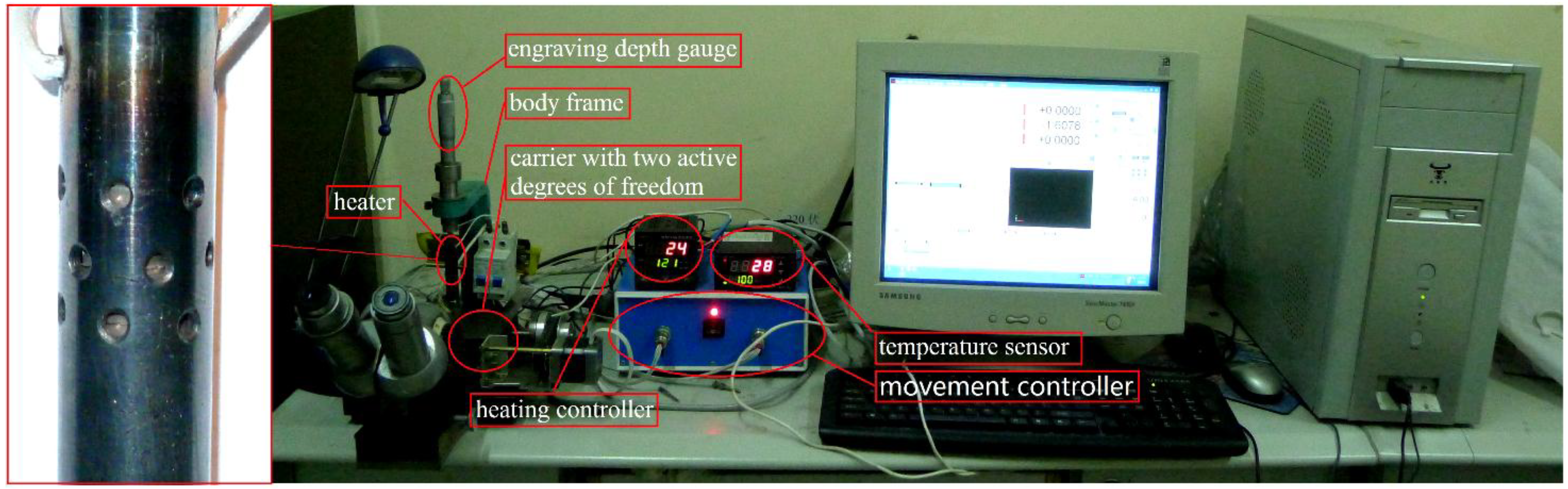
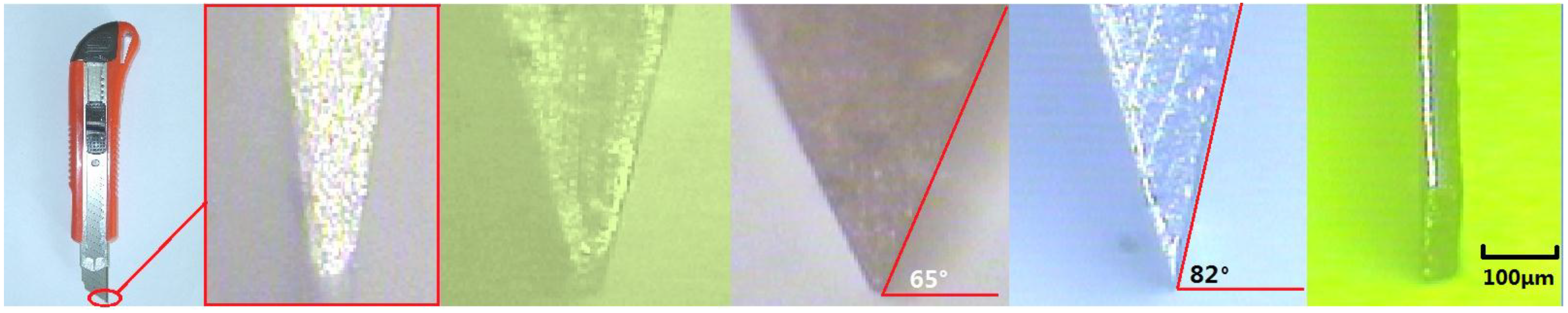
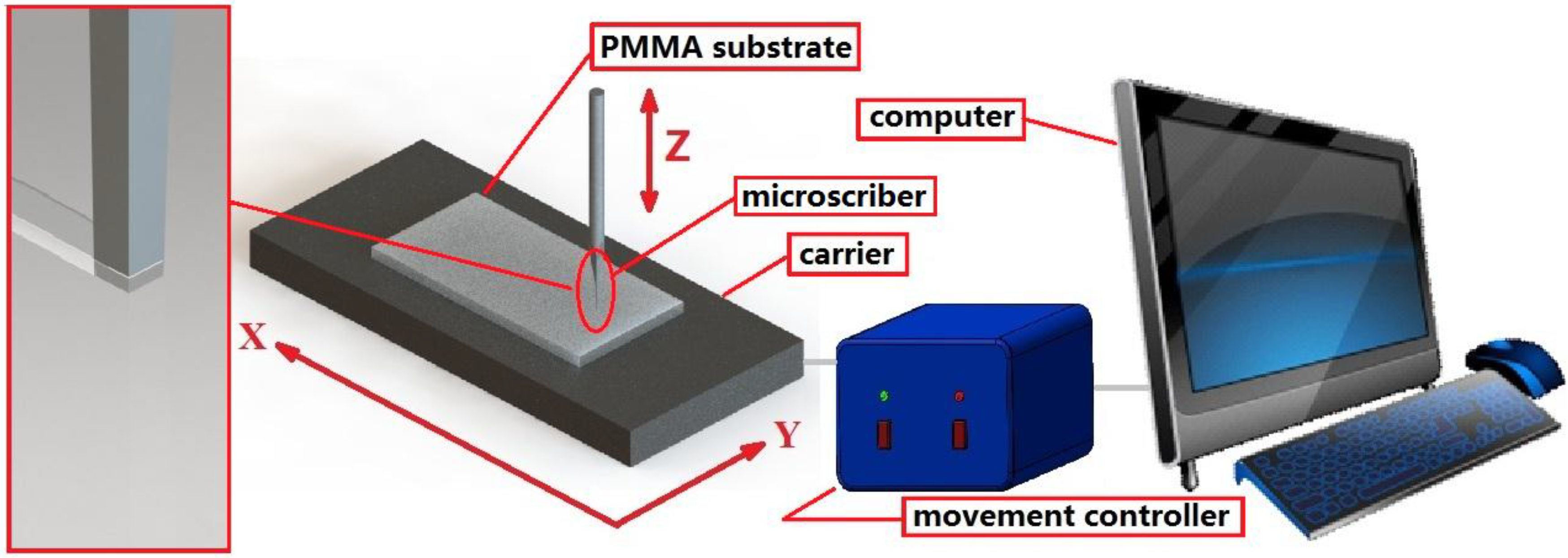
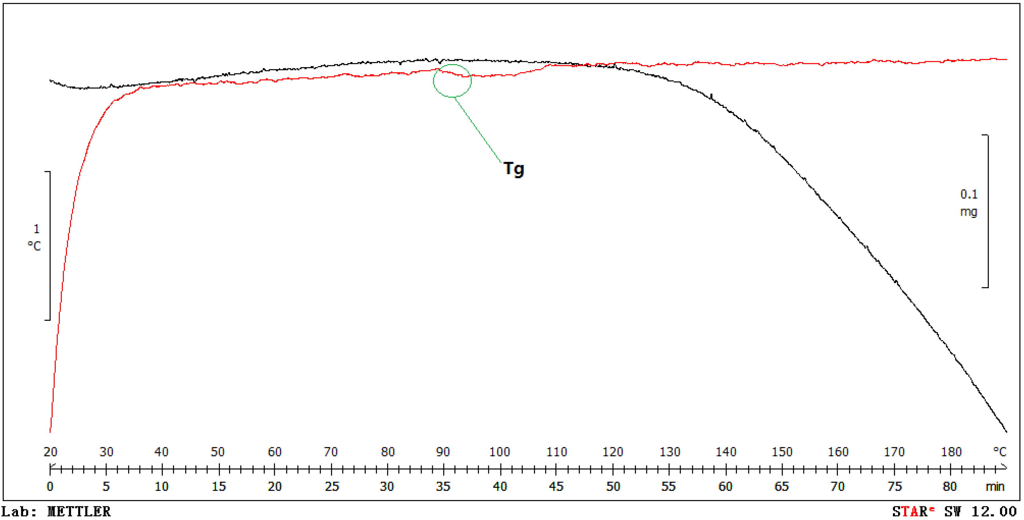
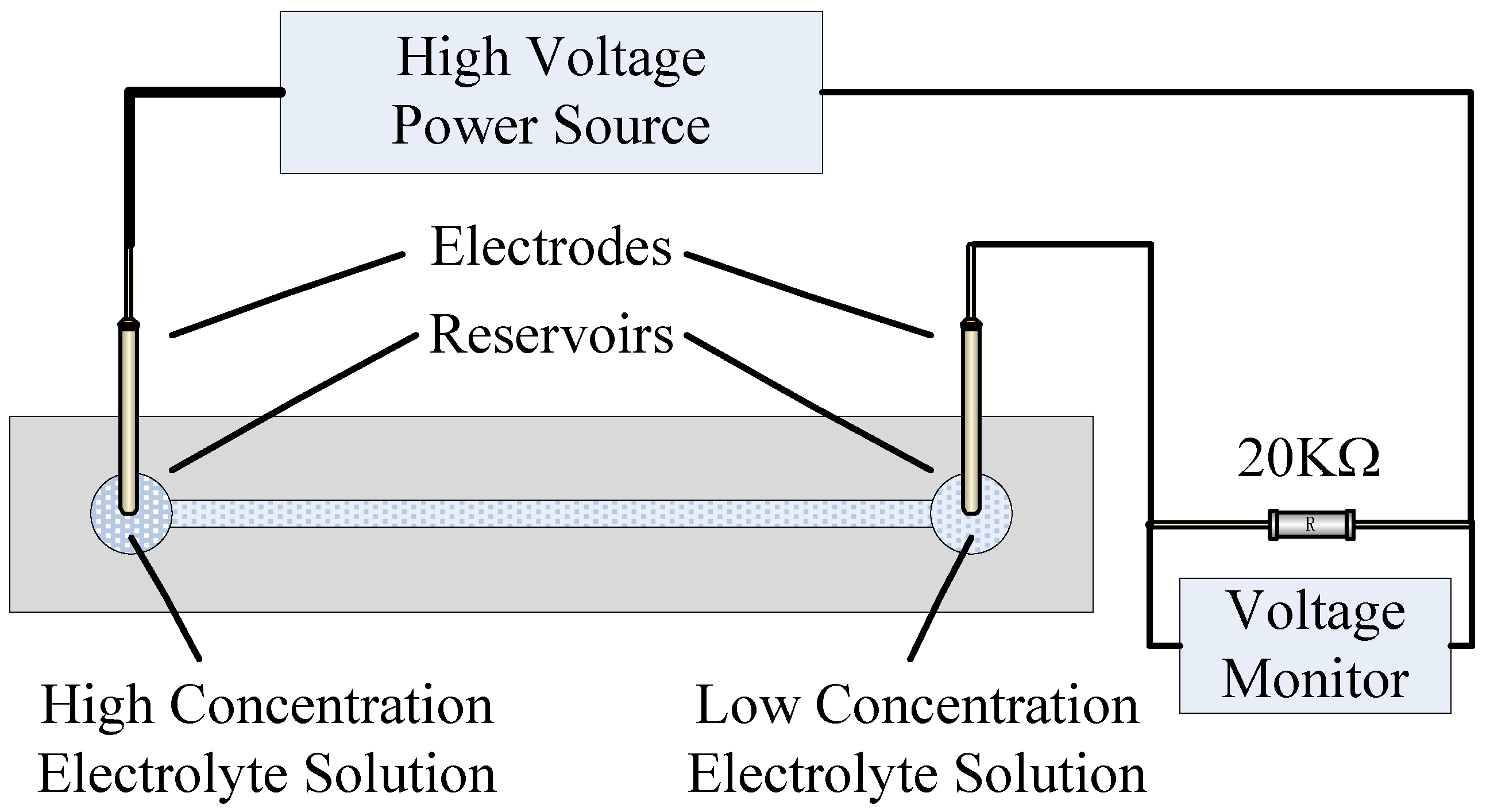
2.1. Experimental Details

The composition of equipment is shown in Figure 1. The equipment constitutes a computer, controllers and the machine tool. The computer is used for designing the patterns of microchannels. Then, software could transfer these designs to the movement controller to fabricate microchannels. There are two controllers in this equipment, one used to control the temperature of the heater and the other used to control the movement of the carrier. The temperature controller consists of a proportion, integration, differentiation (PID) controller and a K-type thermocouple, which could provide a temperature measurement ranging from −40 °C–1200 °C (XMT615, Shanghai Hutuan Instrument Cable Co., Ltd. Shanghai, China). Furthermore, the fluctuation of temperature could be controlled at the level of ±1 °C in self-adjusting mode by the PID controller. The thermal engraving velocity can be controlled at 0.1 mm/s by the controlling stepping motor on the carrier.
Figure 1. The composition of the equipment.
Machines 03 00107 g001
As is seen in Figure 1, the machine tool consists of a body frame, engraving depth gauge, heater, microscriber and carrier with two active degrees of freedom. The body frame serves as a fixed structure, and the engraving depth gauge could be used to control the depth of microchannels. The heater is used to heat the microscriber, and the microscriber is used to fabricate microchannels by the thermal engraving method. The heater is driven by a 220 V alternating current, and its full power is 50 W, which can generate above 400 °C temperatures in the heating zone. We designed a component to fix the heater and manufactured it with steel. Several holes 2 mm in diameter can be observed on the upper side of this part in Figure 1. These small holes are used to dissipate excess heat in case the heat transfers from the heater to other parts of the device during the thermal engraving process. A copper part was employed for good heat transfer between the heater and engraving cutter, and we used precise spark-erosion wire cutting to form a 500 μm wide gap. Effective heat transfer can reduce the temperature gradient from the heater to the head of the grinding cutter. A smaller temperature gradient could raise the maximum temperature of the cutter and form the thermal engraving device fabricating microchannels on polymer whose glass temperature is relatively high. We drilled a 1 mm diameter hole on its side to install a thermocouple. This thermocouple can provide real-time temperature to the PID controller, which is used to adjust the heating process of the heater.
The carrier is controlled by the computer and driven by the movement controller. Furthermore, microchannels could be fabricated on the polymer piece, which is fixed to the carrier. The carrier can move in two horizontal directions, and its velocity is 0–9.9 mm/s. Therefore, the thermal engraving microscriber can be scanned horizontally at a full speed of 9.9 mm/s.
The microscriber was a key part of the machine tool, and it was used to fabricate the microchannels. We chose tungsten steel as the material of the microscriber because of its good hardness and heat conduction. The length of the tungsten steel rod was 10 cm, and its diameter was 3.175 mm. A high precision grinding machine was used to process the microscriber (M820, Dafeng Machinery Co., Ltd. Dafeng, China). The fabricating process of a rectangle microscriber is shown in Figure 2a, and Figure 2b shows a rectangle microscriber after fabrication. In Figure 2b, we put a coin whose diameter is 19.5 mm as a reference. Figure 2c,d is the rectangle microscriber prepared for precision grinding process during the last fabrication step.
Figure 2. Fabricating of a rectangle microscriber. (a) Fabrication process of a rectangle microscriber; (b) A rectangle microscriber after fabrication; (c) A rectangle microscriber prepared for the precision grinding process during the fabrication step; (d) A rectangle microscriber prepared for the precision grinding process during the last fabrication step.
Machines 03 00107 g002
Before grinding the microscriber, we should process a customized fixture, as Figure 3 shows. In this figure, there are several narrow grooves, which can clamp tungsten steel rods when the two parts of the fixture are fastened by crews. We also drilled some via holes on the bodies of two parts of the fixture. The 20 via holes were used to install screws, which can fasten two parts of the fixture and prevent the tungsten steel rods from being thrown out during grinding. The fixture was made of iron, which offers effective ferromagnetism properties, so it could be fixed to the precision grinding machine safely. The tungsten steel rod could be ground into several shapes according to the microchannels we require.
Figure 3. The customized fixture. (a) Exploded diagram of the fixture design; (b) Fixed tungsten steel rods prepared for the precision grinding process.
Machines 03 00107 g003
The fixture is released after each step, so that we could rotate these rods under a microscope between the two grinding processes (XTT, Shanghai Qinfen No. 4 Instrument Co., Ltd. Shanghai, China). The marks on the lens of the microscope could help us rotate the rods to the proper position that we need. Then, the fixture is fastened and prepared for the next grinding process. The tungsten steel rod is cut according to the desired length after grinding, and the procedure for machining a thermal grinding cutter is then complete. Figure 4a is a triangle microscriber, which is adjusted under a microscope, and Figure 4b shows a rectangle microscriber.
Figure 4. Adjusting microscope under microscope. (a) A triangle microscriber adjustment process under a microscope; (b) A rectangle microscriber adjustment process under a microscope.
Machines 03 00107 g004
We can see the micrograph of trapezoid, rectangle and triangle microscribers in Figure 5. Additionally, we included a micrograph of a paper knife for comparison.
Figure 5. Micrograph of different shapes of the engraving microscriber.
Machines 03 00107 g005

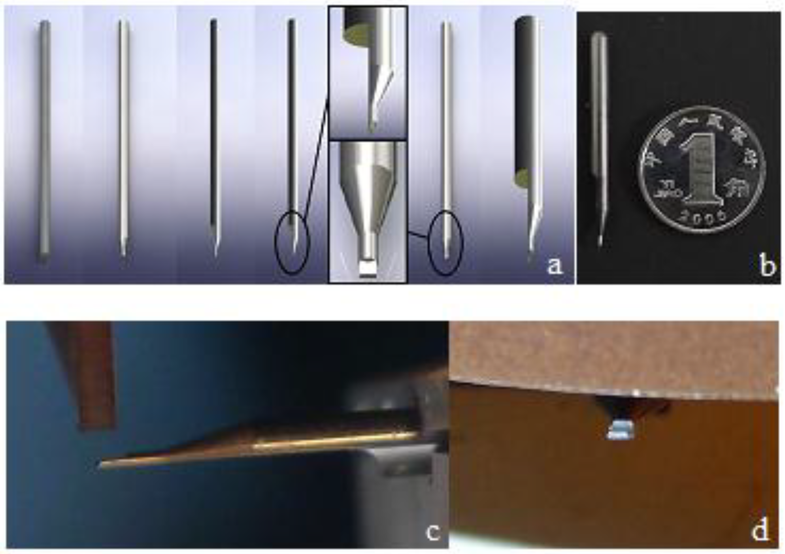
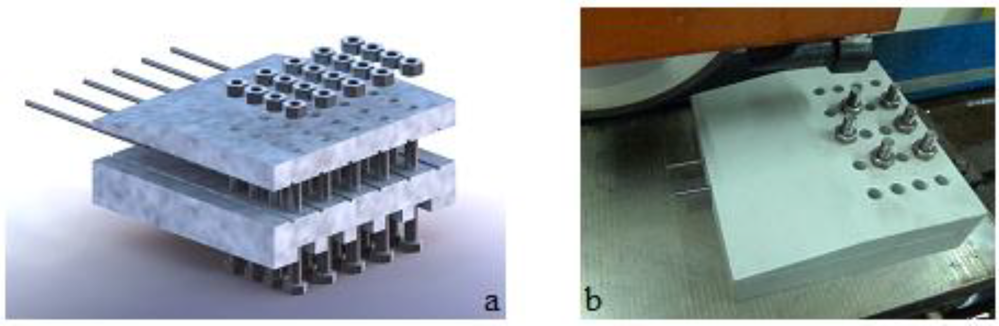
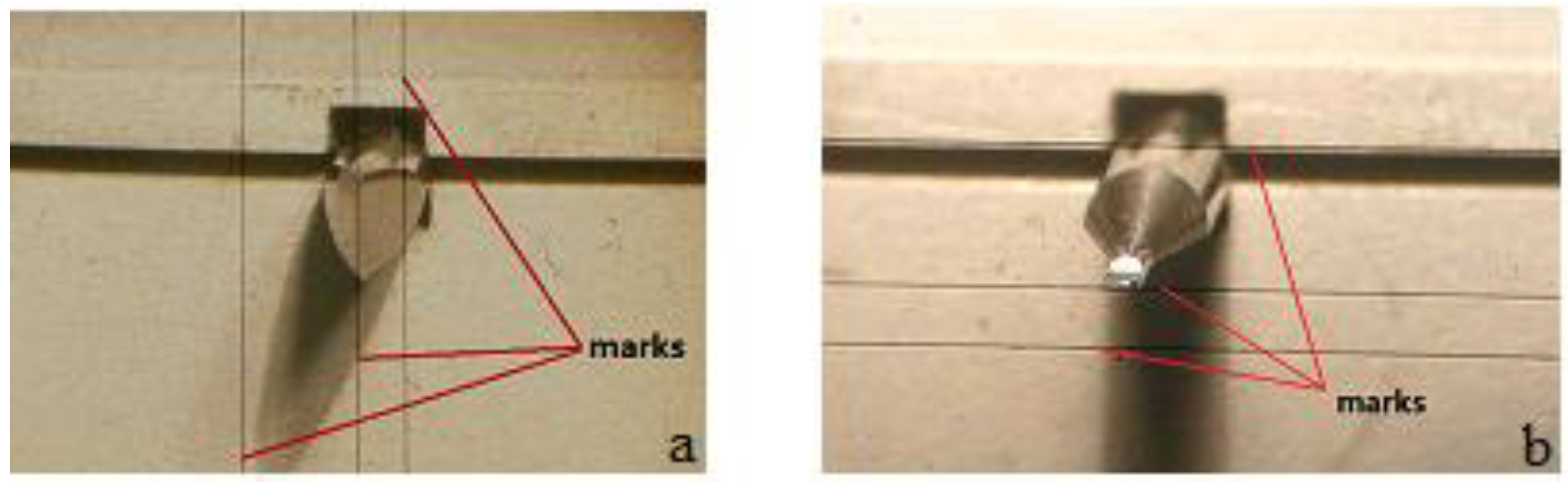
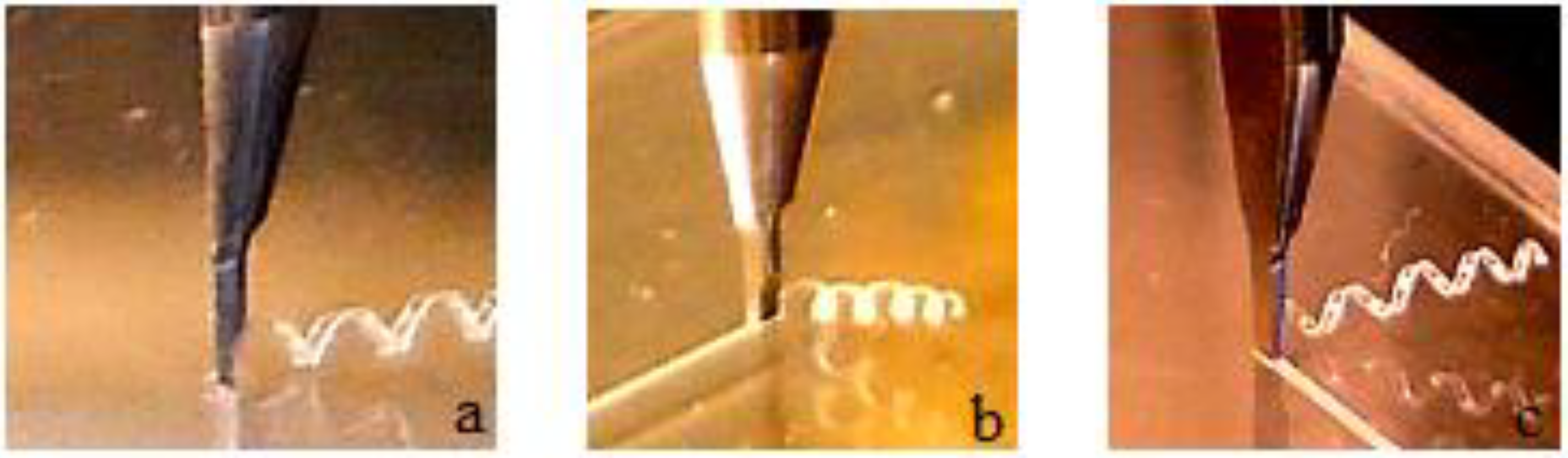
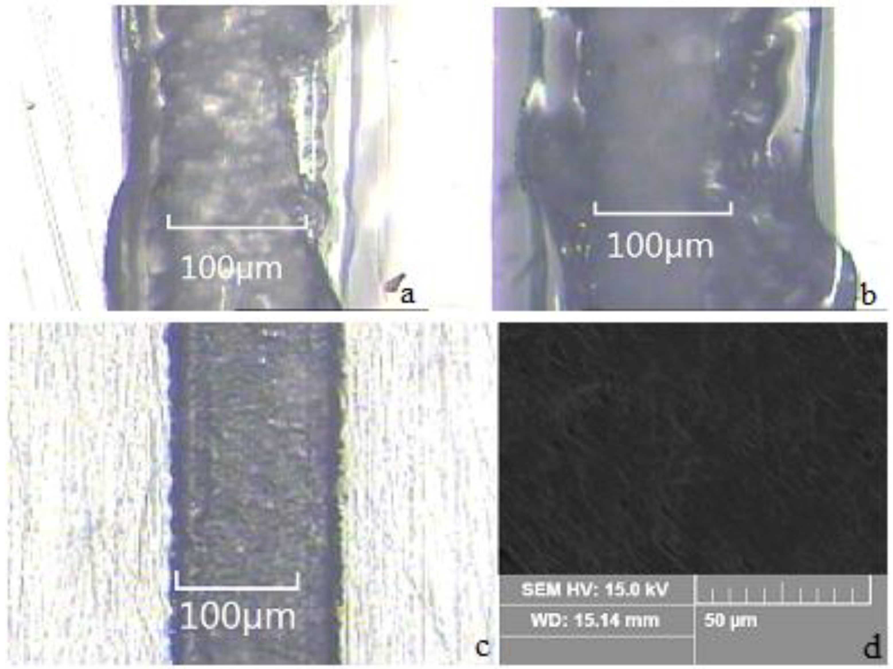
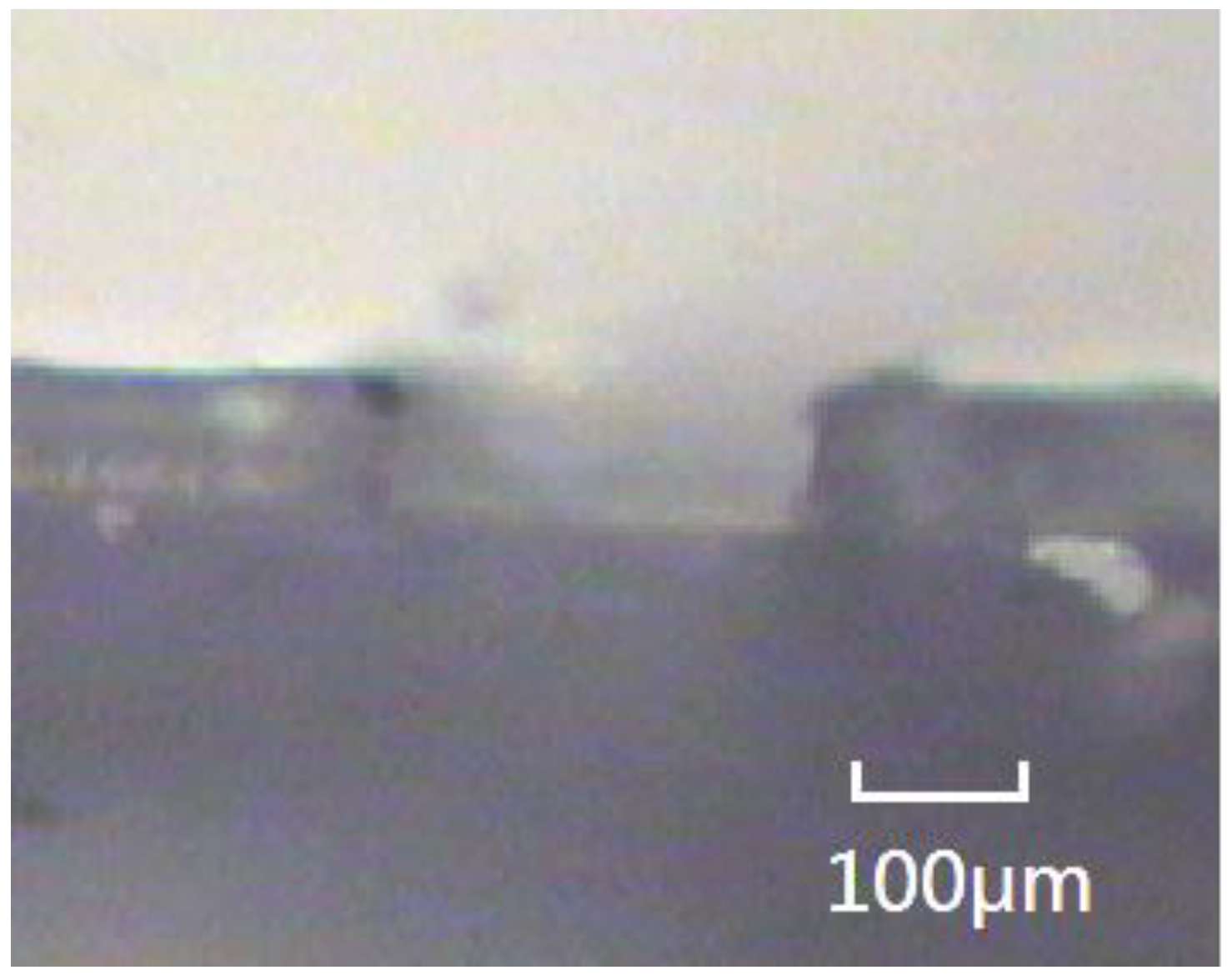
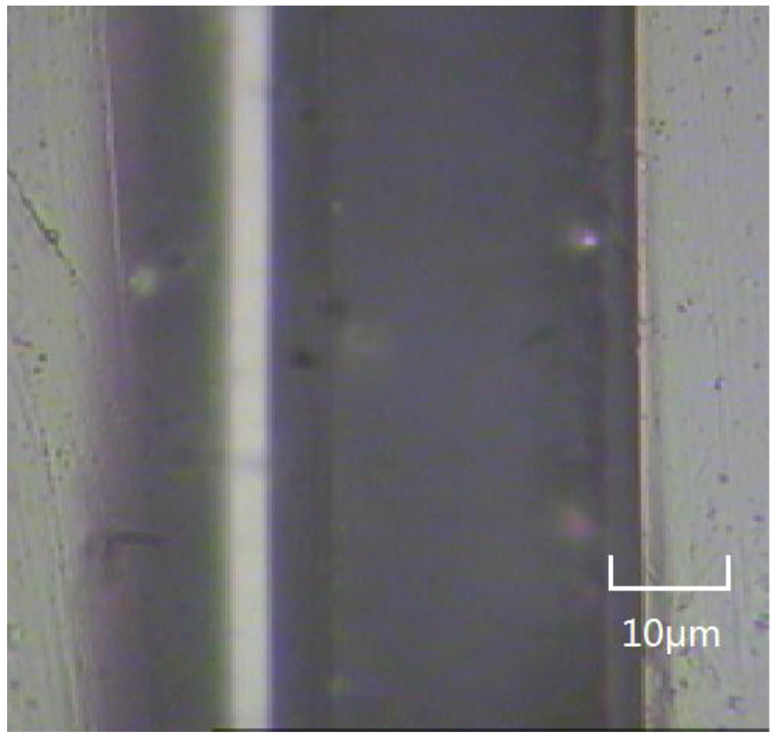
2.2. Microchannel Fabrication

A typical 3 mm-thick PMMA plate was used in our experiment (Stone into Gold Trading Co., Ltd. Dongguan, China). Then, we cut the plate into 10 × 10 cm square pieces to fabricate microchannels on its surface by the CO2 laser. The designed microchannel pattern was put into the software Mach 2 before fabrication. Then, after fixing the PMMA piece on the carrier, the equipment was opened. Proper groups of parameters could produce microchannels with smooth sidewalls and no deformation shape of the cross-section, because our research aimed at improving the roughness of the microchannels. When the microscriber had been heated to a specified temperature, we ran the software. Then, the signal was transferred to the controller, and the controller drove stepping motors, which were fixed on the carrier. Finally, we obtained the microchannels that we designed. Figure 6 shows the procedure as outlined above. The depth of the microchannels is controlled by turning the engraving depth gauge during the fabrication process.
Figure 6. Fabrication schematic diagram.
Machines 03 00107 g006
Figure 7 shows the details of the fabrication process. We could see the engraving microscriber squeezing out polymer melt in the forward direction. The polymer melt is twisted into a spiral at room temperature. After fabricating, the microfluidic chip with microchannels was cut from the PMMA plate and washed with deionized water. Then, it was dried in a vacuum drier and cleaned by compressed nitrogen to remove particles. Thus, a piece of PMMA slice with microchannel patterns was obtained.
Figure 7. Details of the fabrication process. (a) A rear view of the fabrication process; (b) A right view of the fabrication process; (c) A left view of the fabrication process.
Machines 03 00107 g007

3. Results and Discussion

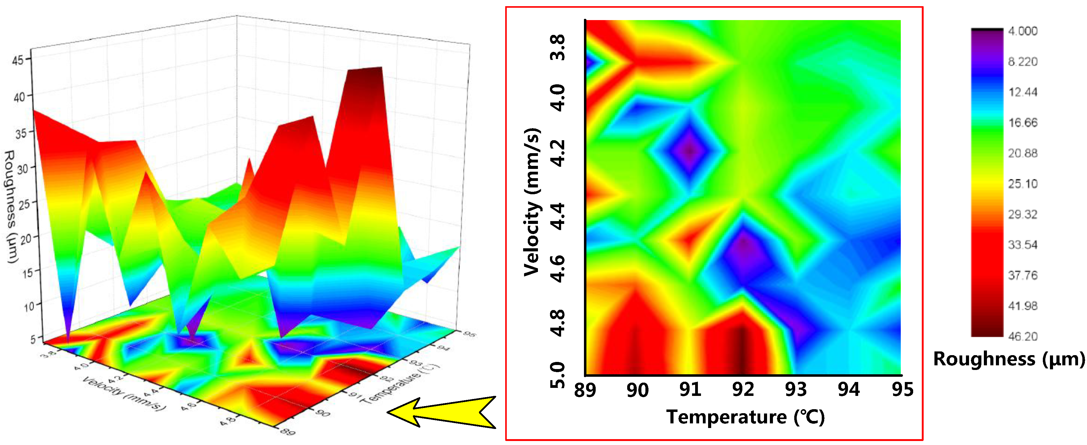
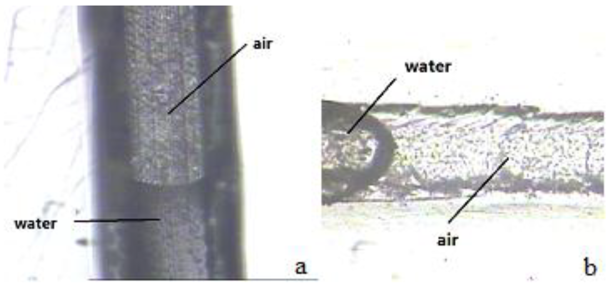
3.1. Effect of Thermal Engraving Velocity and Temperature on Roughness

Thermal engraving velocity and temperature have significant effects on the roughness of microchannels. In this part, we examine the fabrication results for a typical 100 μm width rectangle microchannel. During the comparison of the roughness of microchannels fabricated using different sets of parameters, we could confirm from our experiments that microchannels are much smoother at lower velocity and temperature than at higher velocity and temperature. Figure 8 is a TG-DTA (thermo gravimetric analysis-differential thermal analysis) (TGA/SDTA851e, Mettler-Toledo International Inc., Greifensee, Switzerland) graph. We can see that the glass transition temperature (Tg) of PMMA material is almost 91 °C in Figure 8. Figure 9 shows that the range of heating temperatures of the thermal engraving microscriber is 89 °C–95 °C, with an increasing velocity from 3.7–5 mm/s.
Figure 8. TG-DTA analysis of PMMA.
Machines 03 00107 g008
Figure 9. Effect of thermal engraving velocity and temperature on roughness in a 100 μm width microchannel.
Machines 03 00107 g009
Figure 9 also shows the relationships between the temperature of the thermal engraving microscriber, the thermal engraving velocity and the roughness of the microchannels. We find that smoother microchannels are obtained with a wide velocity range at a lower thermal engraving temperature. Then, the smooth area decreases when microchannels are fabricated under conditions of higher temperatures and velocities compared with microchannels that are fabricated under conditions of lower temperatures and velocities. Several factors lead to this result. Firstly, a higher temperature can increase the amount of free volume available and the intermolecular interactions of molecules [33]. This means that the viscosity is decreased at higher temperatures beyond the limit for the glass temperature of PMMA [33,34]. Secondly, a higher thermal engraving temperature can increase the melting region around the microscriber at the same engraving velocity. This is because higher thermal engraving temperatures can enlarge the temperature difference between the microscriber and PMMA piece. That means more heat transfer occurs from the microscriber to the region of the PMMA piece, which is close to the microscriber in the same period of time. Thirdly, the viscosity of melt is increased as the thickness of the melt layer becomes thinner due to the micro-scale effect [35]. Hence, we can deduce that the melt viscosity is higher than the large-scale flow around the microscriber. The higher viscosity of PMMA melt brings lower flow ability. Furthermore, the lower flow of PMMA melt could be more propitious for defining the parameters during the fabrication of microchannels. Thus, smooth channels are much more difficult to fabricate in the area where the thermal engraving temperature and engraving velocity parameters are high, as shown in Figure 9. However, we still obtain a smooth microchannel in the No. 3 area, and the thermal engraving velocity is higher than in others areas. This is because increasing the velocity of thermal engraving may offset the increasing flow ability of the PMMA melt layer around the microscriber at higher temperature during the fabrication process. However, when the shear stress overcomes the combined force of the entangled molecular chain, slip happens in the lubricating layer [33], while shear-thinning characteristics can decrease the viscosity around the microscriber [33]. Therefore, the fabricating conditions for smooth microchannels are much more difficult to control in the area where the thermal engraving temperature and engraving velocity are both high. Thus, we can see that the smooth area is least in No. 3 in Figure 9. As usual, we chose the No. 1 area parameters as the optimal fabricating conditions due to the stabilization of control.
We cannot obtain smooth channels outside the velocity and temperature range shown in Figure 9. When the temperature is below 89 °C, the temperature of the microscriber is below the lower limit of the glass temperature of PMMA. Therefore, there is no viscous flow to squeeze out in the direction of movement of the microscriber. While we fabricated microchannels on PMMA without heating the microscriber, we only got rough microchannels whose edges and bottoms appeared lacerated under a scanning electron microscope (SEM).
Figure 10 shows 130 μm width microchannels fabricated under different conditions using a metallurgical microscope (C3203A, Shanghai Precision Instrument Co., Ltd. Shanghai, China) and SEM (VEGA 3 SBH, Shanghai Tescan Co., Ltd. Shanghai, China). Figure 10a,b shows the microchannel that was fabricated with inappropriate conditions outside the range shown in Figure 9. Figure 10a is a microchannel fabricated without heating; the microscriber engraving the PMMA piece at room temperature. Therefore, we can see that the edges of the microchannel are lacerated under a metallurgical microscope. Figure 10b is a microchannel fabricated at 133 °C. We can see that the edges of the microchannel appear to be in the shape of cooling viscous flow from melt under a metallurgical microscope. Figure 10c is a smooth microchannel fabricated with an engraving velocity of 4.2 mm/s and a temperature of 93 °C. We study the roughness of the microchannel under SEM. Figure 10d shows the details of the bottom of the smooth microchannel whose maximal roughness is 5 μm. We find that the microchannel is much smoother under optimized conditions, as shown in Figure 10c.
At the same temperature, the lower velocity of thermal engraving may lead to excessive polymer melt around the microscriber. Then, excessive melting polymer causes the increase in roughness of the microchannel. The microchannel roughness is similar to that which is shown in Figure 10b. However, the higher velocity of thermal engraving may induce insufficient polymer melt around the microscriber. Therefore, the microscriber would engrave the elastic boundary directly and slit the boundary during the fabrication. This also induces the increased roughness of the microchannel due to elastic boundary slit. Accordingly, the microchannel roughness is similar to that shown in Figure 10a. Figure 11 is the cross-section of a rectangle microchannel, and Figure 12 shows a 30 μm width rectangle microchannel whose size is commensurate with that achieved by some photolithography or laser introduced technologies [36,37]. Moreover, a 30 μm width rectangle microchannel is the smallest obtained during our study.
Figure 10. Microchannels under different fabrication conditions. (a) A microchannel fabricated without heating; (b) A microchannel fabricated at 133 °C; (c) A smooth microchannel fabricated with an engraving velocity of 4.2 mm/s and a temperature of 93 °C; (d) Details of the bottom of the smooth microchannel.
Machines 03 00107 g010
Figure 11. Cross-section of a rectangle microchannel.
Machines 03 00107 g011
Figure 12. A 30 μm width rectangle microchannel.
Machines 03 00107 g012

3.2. Effect of Surface Characteristics on Surface Wettability

Surface characteristics have a great effect on the surface wettability of a microchannel. After two experiments, we successfully evaluated the surface wettability of our microchannel. Firstly, we heated PMMA pieces by a vacuum oven (DZF-6020, Shanghai Jing Hong Laboratory Instrument Co., Ltd. Shanghai, China). As shown in Figure 9, we heated for a duration of 10 s at each temperature point. We decided the length of heating time based on maximum thermal engraving time in the experiments. Then, we cooled down the PMMA pieces to room temperature and prepared them for contact angle (CA) measurement (JC2000C1, Shanghai Powerreach Digital Technology Apparatus Co., Ltd. Shanghai, China). The experiments were carried out by moving PMMA pieces into a suspended ultrapure water droplet and slowly pushing them against the droplet. Then, the droplet was attached to the PMMA pieces’ surface. As we can see in Table 1, the CAs changed only 5% as the heating temperature increased from 89 °C–95 °C. That means that heating has little effect on the surface wettability of the microchannel. Secondly, we measured the flow shape between the liquid phase and gaseous phase crossing in the microchannel with different roughness. Figure 13a shows a smooth microchannel that was fabricated under the proper conditions. We can see the meniscus between the liquid phase and gaseous phase, and the flow shape of ultrapure water shows a hydrophilic feature in the smooth microchannel. On the contrary, Figure 13b shows a rough microchannel, which was fabricated under three different sets of conditions, seen in Figure 9. We cannot see the meniscus between the liquid phase and gaseous phase, and the flow shape of ultrapure water shows a hydrophobic feature in the rough microchannel. The results of our experiments show that the thermal engraving fabricating technology has less effect on the surface wettability of the microchannel under optimized fabricating conditions.
Table 1. The contact angle (CA) change as the heating temperature increasing from 89 °C−95 °C.
Heating Temperature (°C)89909192939495
CAs (°)7777.678.479.179.680.480.8
Figure 13. Surface wettability of microchannels with different roughness. (a) Surface wettability of a smooth microchannel; (b) Surface wettability of a rough microchannels.
Machines 03 00107 g013

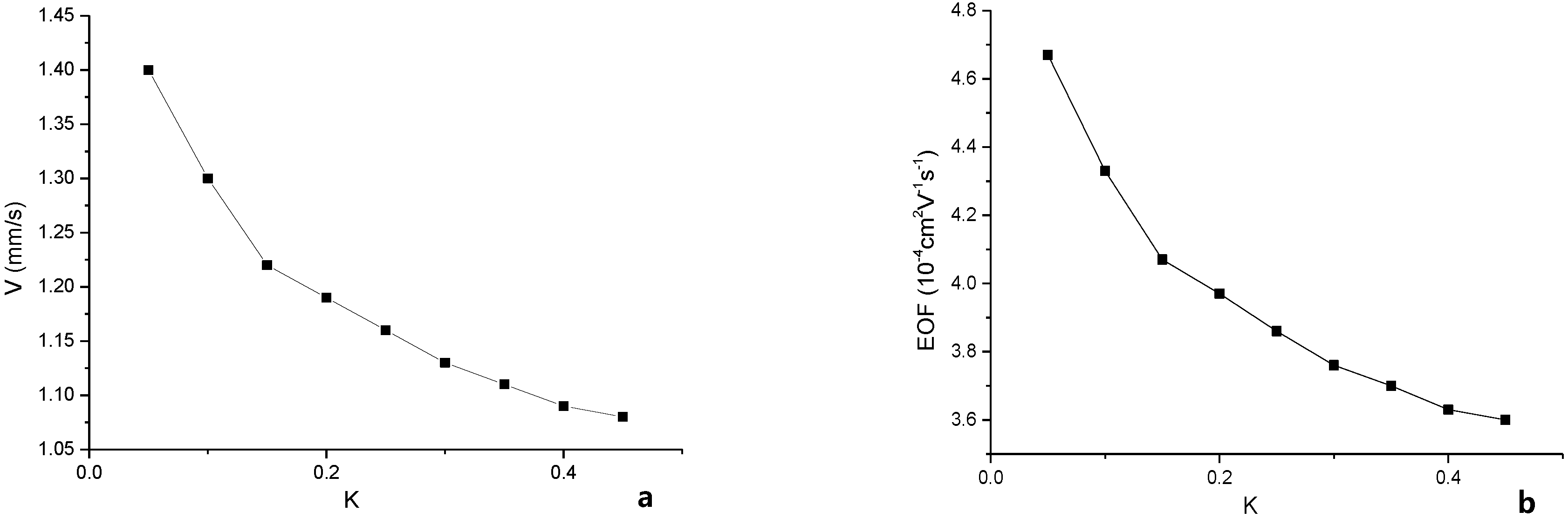
3.3. Effect of Roughness on EOF

Electro-osmotic flow is very important in the microfluidic field. In this experiment, we measured the electro-osmotic flow and the electro-osmotic velocity in microchannels with varied roughness, fabricated using thermal engraving technology. We fabricated several straight microchannels whose cross-sections are all 100 μm wide and 100 μm deep rectangles. Then, we cut them 1 cm in length and drilled two 3 mm diameter holes on the each side of the short microchannels as reservoirs (ZX7025, Hangzhou Shuanglong Machinery Manufacturing Co., Ltd. Hangzhou, China). We filled 20 mmol/L of NaCl electrolyte solution in the microchannel and Reservoir 2 and filled 40 mmol/L of NaCl electrolyte solution in Reservoir 1. Solutions were prepared by using ultrapure water (Laboratory Water Purification System Harbin Yinghua Instrument Co., Ltd. Harbin, China) and NaCl (Tianjin Kermel Chemical Reagent Co., Ltd. Tianjin, China). A high voltage was applied via platinum electrodes in the reservoirs (Shanghai Jiagui Metal Materials Co., Ltd. Shanghai, China). After connecting the two electrodes, a higher voltage was applied by setting Reservoir 2 at a ground potential and Reservoir 1 to a higher voltage (DH1722-6A, Beijing Dahua Radio Instrument Co., Ltd. Beijing, China). Then, the applied high voltage resulted in an electro-osmotic flow in the rectangle microchannel. The 40 mmol/L NaCl solution in Reservoir 1 gradually displaced the 20 mmol/L NaCl solution in the microchannel. Finally, the microchannel solution resistance changed due to concentration changes. Then, the current value was constant. Therefore, the current’s constant value was equal to the time the 40 mmol/L NaCl solution travels from Reservoir 1 to Reservoir 2. We can indicate the average velocity by the length of the microchannel and the current stabilization time. We used the current monitoring method to measure the electro-osmotic flow, and Figure 14 is the schematic diagram (MAS830L, Dongguan MASTACH Instrument Co., Ltd. Dongguan, China). Figure 15a is the electro-osmotic flow (EOF) velocity changes with 100 μm microchannels with different roughness in a 300 V/cm electric field. Figure 15b is the EOF changes with different roughness of 100 μm microchannels in the same electric field. In order to discuss the relationship between EOF characteristics and microchannel roughness, we introduced coefficient K as the ratio of roughness height and microchannel width [38]. Each measurement was repeated six times in our experiments. We found a nonlinear relationship, as shown in Figure 15a,b, since the roughness density was nonlinear as the roughness increased. That means some rough microchannels are still usable due to the nonlinear effect of EOF characteristics.
Figure 14. Measurement of the electro-osmotic flow rate using the current monitoring method.
Machines 03 00107 g014
Figure 15. Electro-osmotic flow (EOF) characteristic changes with roughness for a 100 μm microchannel in a 300 V/cm electric field. (a) EOF velocity changes with different roughness; (b) EOF changes with different roughness.
Machines 03 00107 g015

4. Conclusions

In this paper, we proposed a low-cost and high efficiency method to fabricate microchannels based on PMMA. Then, we researched the relationships among heating temperature, thermal engraving velocity and roughness by means of experiments. Furthermore, optimized processing conditions are ascertained by analyzing a large amount of experimental data. At last, we used a thermal engraving technique to fabricate microchannels, and its characteristics were compared to the performances of some non-lithography techniques. The minimum roughness of microchannels was decreased to 5 μm by adjusting the processing conditions. Meanwhile, the smooth microchannel had good hydrophilic and EOF characteristics. The minimum fabrication width of a rectangle microchannel was ascertained to be 30 μm, which can be compared to some photolithography or laser introduced technologies. Though the rough surface of microchannels is hydrophobic, the relationship between EOF characteristics and roughness was nonlinear due to our fabrication method. The results of our study indicate that the technique proposed achieves good performance and can be used in the microfluidic field, while future investigation into wider applications of this technique for other polymers needs to be continued.

Acknowledgments

This work is supported by the National Natural Science Foundation of China (Grant No. 61404036).

Author Contributions

Xiaowei Han and Li Tian performed the experiments; Xiaowei Han, He Zhang and Zhi-Gang Mao analyzed the data and discuss the results; Xiaowei Han wrote the paper. The project was performed under the directorship and supervision of Xiaowei Liu.

Conflicts of Interest

The authors declare no conflict of interest.

References

  1. Raley, N.F.; Davidson, J.C.; Balch, J.W. Examination of glass-silicon and glass-glass bonding techniques for microfluidic systems. Proc. SPIE 1995, 2639, 40–45. [Google Scholar]
  2. Stjernström, M.; Roeraade, J. Method for fabrication of microfluidic systems in glass. J. Micromech. Microeng. 1998, 8, 33–38. [Google Scholar] [CrossRef]
  3. Chang, T.L. Micromachining of microfluidic channels in glass by microjoule femtosecond laser pulses. Microelectron. Eng. 2013, 110, 450–456. [Google Scholar] [CrossRef]
  4. Becker, H.; Beckert, E.; Gärtner, C. Hybrid tooling technologies for injection molded and hot embossed polymeric microfluidic devices. In Proceedings of the MOEMS-MEMS, San Francisco, CA, USA, 17 February 2010; pp. 1–5.
  5. Kim, D.S.; Kim, J.S.; Ko, Y.B.; Kim, J.D.; Yoon, K.H.; Hwang, C.J. Experimental characterization of transcription properties of microchannel geometry fabricated by injection molding based on Taguchi method. Microsyst. Technol. 2008, 14, 1581–1588. [Google Scholar] [CrossRef]
  6. Hong, T.F.; Ju, W.J.; Wu, M.C.; Tai, C.H.; Tsai, C.H.; Fu, L.M. Rapid prototyping of PMMA microfluidic chips utilizing a CO2 laser. Microfluid. Nanofluid. 2010, 9, 1125–1133. [Google Scholar] [CrossRef]
  7. Huang, Y.; Liu, S.; Yang, W.; Yu, C. Surface roughness analysis and improvement of PMMA-based microfluidic chip chambers by CO2 laser cutting. Appl. Surf. Sci. 2010, 256, 1675–1678. [Google Scholar] [CrossRef]
  8. Romoli, L.; Tantussi, G.; Dini, G. Experimental approach to the laser machining of PMMA substrates for the fabrication of microfluidic devices. Opt. Lasers Eng. 2011, 49, 419–427. [Google Scholar] [CrossRef]
  9. Klank, H.; Kutter, J.P.; Geschke, O. CO2-laser micromachining and back-end processing for rapid production of PMMA-based microfluidic systems. Lab Chip 2002, 2, 242–246. [Google Scholar] [CrossRef] [PubMed]
  10. Chung, C.K.; Lin, S.L. On the fabrication of minimizing bulges and reducing the feature dimensions of microchannels using novel CO2 laser micromachining. J. Micromech. Microeng. 2011, 21, 1–7. [Google Scholar] [CrossRef]
  11. Cheng, J.Y.; Wei, C.W.; Hsu, K.H.; Young, T.H. Direct-write laser micromachining and universal surface modification of PMMA for device development. Sens. Actuators B Chem. 2004, 99, 186–196. [Google Scholar] [CrossRef]
  12. De Marco, C.; Eaton, S.M.; Martinez-Vazquez, R.; Rampini, S.; Cerullo, G.; Levi, M.; Turri, S.; Osellame, R. Solvent vapor treatment controls surface wettability in PMMA femtosecond-laser-ablated microchannels. Microfluid. Nanofluid. 2013, 14, 171–176. [Google Scholar] [CrossRef]
  13. Muluneh, M.; Issadore, D. Hybrid soft-lithography/laser machined microchips for the parallel generation of droplets. Lab Chip 2013, 13, 4750–4754. [Google Scholar] [CrossRef] [PubMed]
  14. Attia, U.M.; Marson, S.; Alcock, J.R. Micro-injection moulding of polymer microfluidic devices. Microfluid. Nanofluid. 2009, 7, 1–28. [Google Scholar] [CrossRef] [Green Version]
  15. Fu, G.; Tor, S.B.; Hardt, D.E.; Loh, N.H. Effects of processing parameters on the micro-channels replication in microfluidic devices fabricated by micro injection molding. Microsyst. Technol. 2011, 17, 1791–1798. [Google Scholar] [CrossRef]
  16. Marson, S.; Attia, U.M.; Lucchetta, G.; Wilson, A.; Alcock, J.R.; Allen, D.M. Flatness optimization of micro-injection moulded parts: The case of a PMMA microfluidic component. J. Micromech. Microeng. 2011, 21, 1–9. [Google Scholar] [CrossRef]
  17. McCormick, R.M.; Nelson, R.J.; Alonso-Amigo, M.G.; Benvegnu, D.J.; Hooper, H.H. Microchannel electrophoretic separations of DNA in injection-molded plastic substrates. Anal. Chem. 1997, 69, 2626–2630. [Google Scholar] [CrossRef] [PubMed]
  18. Tosello, G.; Marinello, F.; Hansen, H.N. Characterisation and analysis of microchannels and submicrometre surface roughness of injection moulded microfluidic systems using optical metrology. Plast. Rubber Compos. 2012, 41, 29–39. [Google Scholar] [CrossRef]
  19. Matteucci, M.; Christiansen, T.L.; Tanzi, S.; ØStergaard, P.F.; Larsen, S.T.; Taboryski, R. Fabrication and characterization of injection molded multi levelnano and microfluidic systems. Microelectron. Eng. 2013, 111, 294–298. [Google Scholar] [CrossRef]
  20. Redha, Z.M.; Baldock, S.J.; Fielden, P.R.; Goddard, N.J.; Treves Brown, B.J.; Haggett, B.G.D.; Andres, R.; Birch, B.J. Hybrid microfluidic sensors fabricated by screen printing and injection molding for electrochemical and electrochemiluminescence detection. Electroanalysis 2009, 21, 422–430. [Google Scholar] [CrossRef]
  21. Mair, D.A.; Geiger, E.; Pisano, A.P.; Fréchet, J.M.J.; Svec, F. Injection molded microfluidic chips featuring integrated interconnects. Lab Chip 2006, 6, 1346–1354. [Google Scholar] [CrossRef] [PubMed]
  22. Mathur, A.; Roy, S.S.; Tweedie, M.; Mukhopadhyaya, S.; Mitra, S.K.; McLaughlin, J.A. Characterisation of PMMA microfluidic channels and devices fabricated by hot embossing and sealed by direct bonding. Curr. Appl. Phys. 2009, 9, 1199–1202. [Google Scholar] [CrossRef]
  23. Tarik, B.H.; Wirth, T.; Gross, T.; Treu, D.; Sahre, M.; Theisen, J. Determination of wettability of surface-modified hot-embossed polycarbonate wafers used in microfluidic device fabrication via XPS and ToF-SIMS. Surf. Interface Anal. 2008, 40, 358–363. [Google Scholar] [CrossRef]
  24. Qi, S.; Liu, X.; Ford, S.; Barrows, J.; Thomas, G.; Kelly, K.; McCandless, A.; Lian, K.; Goettert, J.; Soper, S.A. Microfluidic devices fabricated in poly (methyl methacrylate) using hot-embossing with integrated sampling capillary and fiber optics for fluorescence detection. Lab Chip 2002, 2, 88–95. [Google Scholar] [CrossRef] [PubMed]
  25. Du, L.; Liu, C.; Liu, H.; Qin, J.; Wei, Y. Micro Hot Embossing Metal Mold For Microfluidic Chip Based On No Back Plate Growing Method. In Proceedings of the 1st IEEE International Conference on Nano/Micro Engineered and Molecular Systems, 2006 (NEMS’06), Zhuhai, China, 18–21 January 2006; pp. 101–104.
  26. Lei, K.F.; Li, W.J.; Yam, Y. Effects of contact-stress on hot-embossed PMMA microchannel wall profile. Microsyst. Technol. 2005, 11, 353–357. [Google Scholar] [CrossRef]
  27. Li, J.M.; Liu, C.; Peng, J. Effect of hot embossing process parameters on polymer flow and microchannel accuracy produced without vacuum. J. Mater. Process. Technol. 2008, 207, 163–171. [Google Scholar] [CrossRef]
  28. Youn, S.W.; Noguchi, T.; Takahashi, M.; Maeda, R. Fabrication of micro mold for hot-embossing of polyimide microfluidic platform by using electron beam lithography combined with inductively coupled plasma. Microelectron. Eng. 2008, 85, 918–921. [Google Scholar] [CrossRef]
  29. Nugen, S.R.; Asiello, P.J.; Baeumner, A.J. Design and fabrication of a microfluidic device for near-single cell mRNA isolation using a copper hot embossing master. Microsyst. Technol. 2009, 15, 477–483. [Google Scholar] [CrossRef]
  30. Koerner, T.; Brown, L.; Xie, R.; Oleschuk, R.D. Epoxy resins as stamps for hot embossing of microstructures and microfluidic channels. Sens. Actuators B Chem. 2005, 107, 632–639. [Google Scholar] [CrossRef]
  31. Chen, Z.; Zhang, L.; Chen, G. A spring-driven press device for hot embossing and thermal bonding of PMMA microfluidic chips. Electrophoresis 2010, 31, 2512–2519. [Google Scholar] [CrossRef] [PubMed]
  32. Yeo, L.P.; Ng, S.H.; Wang, Z.F.; Xia, H.M.; Wang, Z.; Thang, V.S. Investigation of hot roller embossing for microfluidic devices. J. Micromech. Microeng. 2010, 20, 1–10. [Google Scholar] [PubMed]
  33. Lin, X.; Kelly, A.; Woodhead, M.; Ren, D.; Wang, K.; Coates, P. Capillary study on geometrical dependence of shear viscosity of polymer melts. J. Appl. Polym. Sci. 2014, 1–10. [Google Scholar]
  34. Kobayashi, H.; Takahashi, H.; Hiki, Y. Viscosity measurement of organic glasses below and above glass transition temperature. J. Non-Cryst. Solids 2001, 290, 32–40. [Google Scholar] [CrossRef]
  35. Wang, L.; Li, Q.; Zhu, W.; Shen, C. Scale effect on filling stage in micro-injection molding for thin slit cavities. Microsyst. Technol. 2012, 18, 2085–2091. [Google Scholar] [CrossRef]
  36. Salih, N.M.; Nafarizal, N.; Soon, C.F.; Sahdan, M.Z.; Tijjani, A.; Hashim, U. Glass etching for cost-effective microchannels fabrication. In Proceedings of 2014 IEEE International Conference on the Semiconductor Electronics (ICSE), Kuala Lumpur, Malaysia, 27–29 August 2014; pp. 432–435.
  37. Prakash, S.; Kumar, S. Fabrication of microchannels on transparent PMMA using CO2 Laser (10.6 μm) for microfluidic applications: An experimental investigation. Int. J. Precis. Eng. Manuf. 2015, 16, 361–366. [Google Scholar] [CrossRef]
  38. Liu, Y.; Yang, D. Effect of Wall Roughness on Electro-Osmotic Flow in Microchannels. In Advanced Tribology; Springer: Berlin/Heidelberg, Germany, 2010; pp. 588–591. [Google Scholar]

