Article

Fabrication of Single Crystals through a µ-Helix Grain Selection Process during Electron Beam Metal Additive Manufacturing

by
Martin R. Gotterbarm
1,2,*,
Alexander M. Rausch
2 and
Carolin Körner
1,2
1
Joint Institute of Advanced Materials and Processes, University of Erlangen-Nürnberg, Dr.-Mack-Str. 81, 90762 Fürth, Germany
2
Chair of Materials Science and Engineering for Metals, University of Erlangen-Nürnberg, Martensstr. 5, 91058 Erlangen, Germany
*
Author to whom correspondence should be addressed.
Metals 2020, 10(3), 313; https://doi.org/10.3390/met10030313
Submission received: 13 January 2020 / Revised: 26 February 2020 / Accepted: 26 February 2020 / Published: 28 February 2020
(This article belongs to the Special Issue Metal Additive Manufacturing – State of the Art 2020)

Abstract

:
Selective Electron Beam Melting (SEBM) is a powder bed-based additive manufacturing process for metals. As the electron beam can be moved inertia-free by electromagnetic lenses, the solidification conditions can be deliberately adjusted within the process. This enables control over the local solidification conditions. SEBM typically leads to columnar grain structures. Based on numerical simulation, we demonstrated how technical single crystals develop in IN718 by forcing the temperature gradient along a µ-Helix. The slope of the µ-Helix, i.e., the deviation of the thermal gradient from the build direction, determined the effectiveness of grain selection right up to single crystals.

1. Introduction

Additive Manufacturing (AM) is an integral part of Industry 4.0, the fourth industrial revolution. AM is a revolutionary way of manufacturing, and is thus subject to intense research and development efforts. With respect to powder bed fusion AM of metals, Selective Electron Beam Melting (SEBM) and the more common Selective Laser Melting (SLM) were investigated. The use of an electron beam as a heat source offers unique possibilities for the manufacturing process. Namely, operating temperatures of more than 1000 °C become feasible as the electron beam can not only be used in a focused way for selective melting. The defocused beam can also be used as a source of global heat input. This makes SEBM suitable for processing of the most challenging materials like nickel- and cobalt-based superalloys or intermetallics, such as titanium aluminides [1]. As the grain structure governs the mechanical properties, it is highly desirable to control or manipulate the developing grain structure within any manufacturing process. SEBM typically yields a columnar grain structure, resulting in a highly anisotropic mechanical behavior [2,3,4]. The elongated grains originate from epitaxial growth and steep temperature gradients oriented mostly parallel to the build direction (BD) [3,5,6,7]. However, the grain structure can be manipulated by altering the SEBM processing strategy, and thus influencing the solidification conditions. The possibility of tailoring the grain structure towards a more equiaxed one has been demonstrated in various publications [8,9,10]. For extremely demanding applications like turbine blades, single crystalline parts are state-of-the-art. Until now, the successful generation of single crystals via SEBM has only been reported by Ramsperger et al. [11] and Chauvet et al. [12], and the underlying mechanisms are not yet fully understood. This study aims to provide a deeper understanding of the underlying grain selection processes leading to single crystals. The nickel-based superalloy IN718 was used as the model alloy to fabricate technical single crystals via SEBM. The solidification conditions were subsequently analyzed using numerical simulations of the process.

2. Materials and Methods

In the present study, trapezoidal prisms, as depicted in Figure 1b, were fabricated from IN718 powder on an Arcam A2 machine (Arcam AB, Mölndal, Sweden), which was modified to meet the specifications of an Arcam A1. As a scan strategy, cross snake hatching (CS, see Figure 1a) without contour melting was used for all samples. The SEBM processing parameters are listed in Table 1 and originate from prior processing window experiments. Two different variations of CS were employed. On the one hand, a standard hatching (SH) approach with a moderate line offset of 100 µm, and a scan speed of 3 m/s was used. On the other hand, the multi passing (MPCol) strategy introduced by Helmer et al. [8] was employed, where small line offsets and high scan speeds are used. The µ-Helix parameter setting is a special variant of multi passing, which enables controlling the solidification paths to resemble a µm-sized helix. Three trapezoidal prisms with varying aperture angles in the wedge section were manufactured with each parameter setting. A total of nine samples were built. Note, that the samples were rotated by 45° with respect to the scan vectors SX and SY, in order to achieve a constant scan length of 15 mm in the middle of the sample. Additionally, cuboid samples with the dimensions 15 × 15 × 120 mm³ (XYZ) were manufactured with the µ-Helix parameter setting for comparison. In this case, the edges of the cuboids were aligned with the scan vectors. As a start plate, a polycrystalline IN718 disk with a thickness of 16 mm, and a diameter of 136 mm was used. The samples were connected to the start plate via cylindrical support structures. The build temperature was held constant at 950 °C, as measured by a thermocouple attached to the start plate. A build chamber pressure of 2 × 10⁻³ mbar under Helium atmosphere was applied during the build. The raw material IN718 powder, with a particle size distribution of 45–105 μm, was used, provided by TLS Technik GmbH & Co. Spezialpulver, Bitterfeld, Germany. The powder particles showed spherical morphology with few satellites and moderate residual porosity. The chemical composition is given in Table 2. For analysis, all manufactured samples were metallographically prepared as longitudinal microsections. They were subsequently etched with a HCl + H2O2 etching solution to reveal the grain structure. No heat treatments were applied, in order to document the as-built state.
In order to gain further insights into the grain orientation, electron backscatter diffraction (EBSD) measurements were performed on four samples. Multiple mappings from the center of the sample, close to the top surface, were collected with a step size of 5 µm, and subsequently stitched. The measurements and post processing were performed on a Helios NanoLab DualBeam 600 FIB/SEM (FEI Company, Hillsboro, OR, USA) equipped with a NordlysNano EBSD detector using the AZtecHKL and the HKL CHANNEL5 software (Oxford Instruments, Abingdon, UK), as well as the MATLAB toolbox MTEX. In order to allow for a quantitative comparison of the crystallographic texture, the texture index J O D F was computed by MTEX according to Equation (1) [13]:
J O D F = | f ( g ) | 2 d g ,
where f is the orientation distribution function (ODF) that is calculated from the EBSD data, and g represents an orientation. Accordingly, J O D F = 1 for a completely uniform distribution of orientations and it is infinitely large for a single orientation.
Numerical simulations were used to analyze the solidification conditions during SEBM as a function of the processing parameters. The simulations were conducted using the 2D version of our in-house software tool, S A M PLE 2 D (Simulation of Additive Manufacturing on the Powder scale using a Laser or Electron beam), which is described elsewhere in detail [14]. It is based on a Lattice Boltzmann framework that solves full hydrodynamics in the melt pool, and thermodynamics in the entire domain. The setup used in the current study is depicted in Figure 2a, and the used material parameters [15,16,17] are listed in Table 3. As the simulation domain is two dimensional (15 mm width), only rotations of the hatching pattern by 180° are possible. A cell size of 5 × 5 µm2 and a time step of 2 × 10⁻⁷ s were used. The scan vectors, with a length of 15 mm, run perpendicular to the simulation plane. In order to assess the solidification conditions during SEBM without the stochastic influence of powder, a block of solid material with a height of 50 µm was added, instead of placing individual powder particles in each layer. For each parameter setting listed in Table 1, three layers were simulated. While a large quantity of outputs can be sourced from S A M PLE 2 D , the main focus of this study was the thermal gradient G and the solidification interface velocity vs. Both values were taken at the solidification front. This was implemented by tracking the isotherm of the average temperature between solidus and liquidus. The orientation of G plays a key role as it dictates the growth direction of the dendrites during solidification [18]. As depicted in Figure 2b, the maximum deviation of vs from the BD, labeled φint, is always present at the interface between two layers. Consequently, φint was tracked directly at the interface between the first layer and the respective next higher layer.

3. Results and Discussion

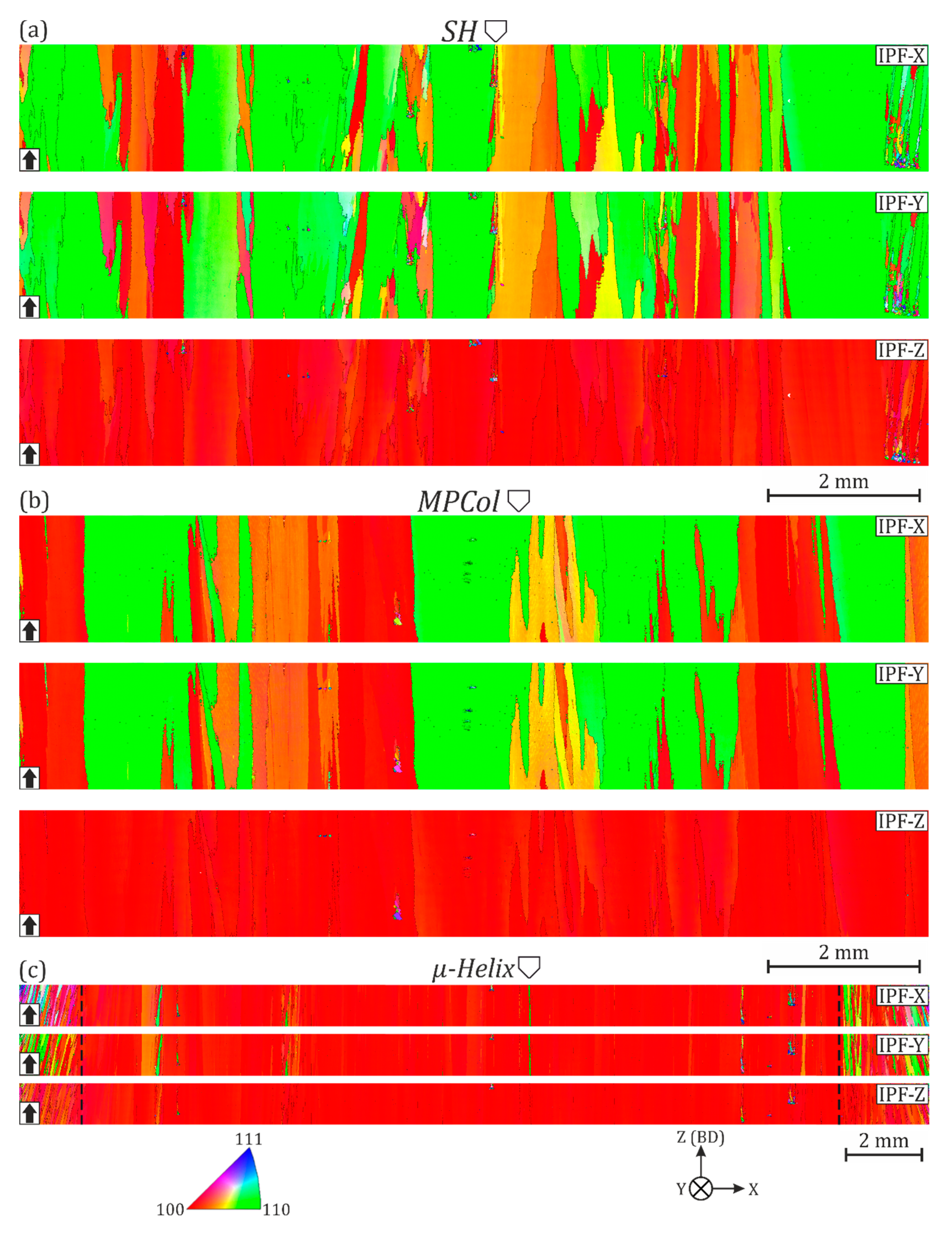
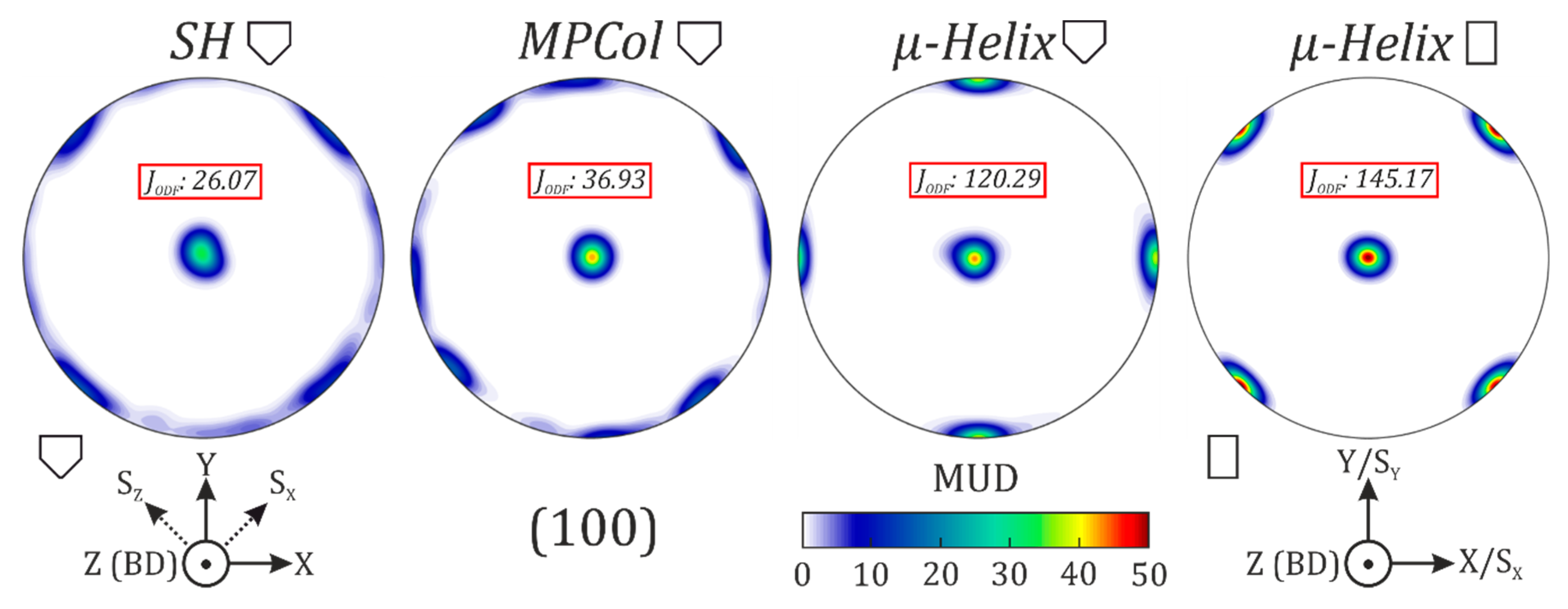
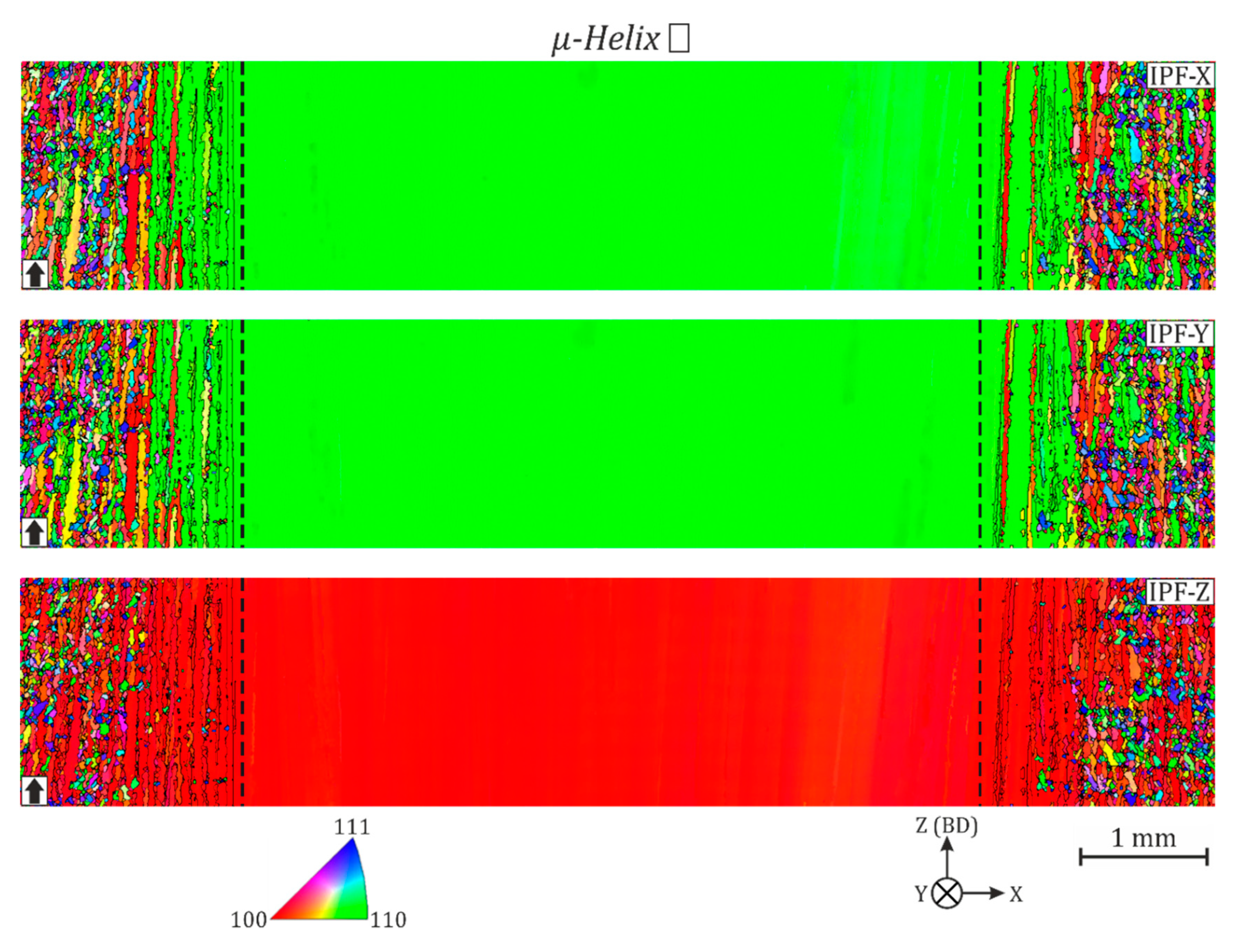
3.1. Grain Structure Characterization

Figure 3 shows overview images of macro etched longitudinal sections of the three different microstructures examined in this study. Deviations from the CAD geometry are mainly due to specimen preparation. The standard hatching strategy (SH) (Figure 3a) leads to a columnar grain structure, with grains growing epitaxially over numerous layers. A certain grain coarsening over the build height is evident. The mean grain width increases from about 100 µm at the very bottom of the sample up to around 500 µm near the top surface. In the vicinity of the side surfaces, the grain structure is dominated by inward growing fine columnar grains, which are triggered by nucleation from the surrounding powder bed. The section is about 1 mm wide, and is a well-known phenomenon in powder bed fusion additive manufacturing [7]. As can be seen from the detailed picture in Figure 3d, the grain boundaries are, overall, clearly aligned parallel to the BD, yet somewhat serrated. The corresponding results from the large area EBSD mappings in Figure 6 provide detailed information about the crystallographic orientation of the grains. The IPF-Z map, where the coloring is chosen according to the BD, is almost solely colored in red, which indicates a very strong <100> fiber texture parallel to the BD. This is quantified by a high texture index of J O D F = 26.07 , whereas a value of 1 represents no texture at all. Minor agglomerations of stray grains can also be observed, but these are quickly overgrown by <100> oriented grains over the course of a few layers. The IPF-X and Y maps show a different picture. Here, green is the predominant color, indicating orientations around <110>. This can be seen even more clearly as distinct peaks in the pole figures, e.g., on the outer rim of the {100} pole figure. It can thus be noted that in addition to the strong anisotropy in the orientation of the primary dendrite arms, there is also anisotropy in the orientation of the secondary dendrite arms. Taking the 45° rotation of the samples with respect to the scan vectors into account, the preferred orientation of the secondary <100> directions coincides with the scan vectors. This grain structure can be seen as the reference grain structure for SEBM-IN718, manufactured with standard cross snake hatching scan strategies, and is comparable to what is reported in the literature [1,5,19,20].
A small line offset combined with a very high scan speed (MPCol) leads to columnar grains, as depicted in Figure 3b. However, the grain selection along the BD is slightly more pronounced here. The grain width increases faster within the first 10 mm of the build compared to SH. From the detailed picture in Figure 3e, it is evident that the grain boundaries are significantly less serrated and generally tend to run more parallel to the BD. Qualitatively, the grain length appears to be larger as well. With an expansion of about 2.5 mm, the region affected by nucleation from the powder bed at the side surfaces is notably enlarged in comparison to SH. This region also exhibits significant notches, which drastically deteriorate the surface quality. This phenomenon can be explained as follows: During hatching, the beam generally passes any given spot on the surface multiple times, due to the fact, that the beam diameter (300–400 µm) is significantly larger than the line offset. Using multi passing, the necessary energy input per area to produce dense materials is higher compared to standard hatching, although the line energies are significantly lower. The first hatch lines within any layer are generally needed to heat up the material and initially form a stable melt pool. The low line energies consequently lead to a prolonged region of reduced melt depth at the beginning of a layer, and may thus cause delamination issues at the edges since no contour melting is applied. In terms of crystallographic texture, the grain structure exhibits similar results in the EBSD measurements compared to the standard hatching sample. The <100> fiber texture is even more pronounced, as indicated by a texture index of 36.93. However, the anisotropy of the secondary dendrite arms is not as distinct, which becomes evident from the more diffuse appearance at the rim of the {100} pole figure.
As can be seen in Figure 3c, a small line offset paired with moderate scan speeds (µ-Helix) allows the realization of technical single crystals (SXs). It is already evident from the macro etched state, that the SX region in the center of the sample, which is about 21 mm wide, is surrounded by a polycrystalline (PX) shell of about 2 mm width, similar to the other samples examined in this study. There are some isolated stray grains present within the SX region, which are overgrown in subsequent layers (see Figure 3f). The orientation of the grains within the first layers is rather randomly distributed due to heterogeneous nucleation from the powder bed [21]. A grain selection region of approximately 9 mm in build height is present at the bottom, until the SX orientation prevails. It is interesting to note, that the shape of the SX-region is similar to the shape of the sample, as the wedged bottom section leads to nucleation from the powder, as long as the cross section of the part is still increasing with the build height. Once the final cross section is established, the SX grain selection process will again take place over the course of the next approximately 9 mm build height. This behavior is also seen in the fabrication of SEBM-CMSX-4 technical single crystal samples [11].
In order to analyze the impact of the part geometry on the grain selection process, trapezoid samples with different aperture angles in the wedge section were manufactured. The corresponding macro-etched longitudinal sections are depicted in Figure 4. Please note, that the notch-like feature seen in Figure 4b is due to an error during sample cutting. In all cases, the grain selection in the sample center takes place within the first 9 mm of build height, regardless of the part geometry. For comparison purposes, large cuboid samples were manufactured with the µ-Helix parameter setting at a later stage, with an improved build temperature control during the process. A macro etched longitudinal section of the lower part of such a cuboid sample is depicted in Figure 5. Again, an SX region is evident in the center of the sample surrounded by a PX shell. The SX region is stable along the whole build height of 120 mm. The section demonstrates the possibility of obtaining large, high quality SX samples with the µ-Helix parameter setting, and the importance of tight temperature control during SEBM build jobs.
While there is no generally accepted definition, technical single crystals typically allow for low angle grain boundaries, with a misorientation angle of up to 10°, to be present within the material. In order to verify the compliance of the presented samples with this requirement, large area EBSD mapping was performed over the whole sample width. The results are shown in Figure 6c and confirm that a technical single crystal was indeed built, albeit flawed. The only grain boundaries exhibiting a misorientation angle of > 10° are the isolated stray grains, and the PX shell, which were both already discussed. Consequently, the texture index of 120.29 within the SX region is extremely high. It should be noted however, that the present stray grains may significantly affect the material’s properties. The results of the EBSD analysis of the SX cuboid sample are depicted in Figure 7 (ODF pole figures) and Figure 8 (IPF maps). This SX exhibits a higher quality by means of the absence of stray grains. Consequently, the texture index within the SX region of 145.17 is even higher compared to the trapezoidal prism SX. The resulting pole figures clearly show that there is only one distinct crystal orientation present in the SX regions. The primary orientation of the dendrites is once again <100> parallel to the BD, analogous to the columnar grain structures. The key difference lies within the uniform orientation of all secondary dendrite arms, which are rotated by 45° with respect to the scan vectors (note the orientation of the samples in the build chamber for the trapezoidal prisms, see Figure 1).

3.2. Numerical Simulation

Numerical simulations of the SEBM process using our in-house software S A M PLE 2 D [14] were performed to reveal the solidification conditions for all hatching strategies. The parameters listed in Table 1 were used. The first aim was to assess the resulting melt pools. This is of particular interest, as the melt pool shape mainly determines the orientation of G during solidification, which is perpendicular to the melt pool walls, as depicted in Figure 2b. It has been proven to play a key role in grain structure formation in SEBM [19]. Figure 9 shows results from the S A M PLE 2 D simulations for the three investigated parameter settings. When comparing the results it is evident, that all melt pools (dark grey) fundamentally exhibit a similar shape, while the size varies. To understand how these rather similarly shaped melt pools can lead to such drastically different grain structures, one has to bare in mind that only a rather small region of interest (ROI) determines the final grain structure, as highlighted in Figure 9. This is due to the fact that the majority of the meltpool will be remelted in subsequent beam passes and layers and, thus, does not contribute to the grain structure of the final part. The height of this ROI is equal to the layer thickness (typically 50 µm) starting from the melt pool bottom. The lateral dimension of the ROI is mainly determined by the line offset, and can be assessed by stringing together a series of melt pools with a distance equal to the line offset. It is evident from these visualizations, that G, on average, diverges from the BD within each layer, as indicated by the solidification paths. One can also derive that the deviation will always start at 0° at the melt pool bottom and increase up to its maximum, φint, at the very top of the ROI as the melt pool curvature increases continuously with the height. In the following, the solidification conditions are analyzed in detail.
We investigated the maximum deviation of G from the BD at the interface between the two layers, φint, for each parameter setting as a function of the lateral position in the part (see Figure 10). The respective moving averages of φint are shown. It is evident, that there is a strong influence of the position in the part φint for all settings. These boundary effects can be understood by considering Figure 10a, where the three simulated layers are arranged schematically, and the respective interface for the evaluation of φint is highlighted. Here, the aforementioned melt pool initialization phase becomes evident: The melt pool depth increases steadily within the first 2–4 mm (depending on the processing parameters), until it reaches equilibrium. This leads to an overmelting effect of preceding layers in the boundary regions, as highlighted in Figure 10c. On the very left side, where the initialization phase of Layer 1 took place, only Layer 2 effectively remains. It overmelts this portion of Layer 1 entirely. As the interface for the evaluation of φint was defined on the basis of Layer 1 and the next higher Layer (see Section 2), φint can not be evaluated here. Consequently, there are no data points available for plotting in Figure 10b. As soon as Layer 1 reaches a sufficient melt depth, φint increases at the melt depth. Once a stable melt pool with a constant melt depth is established, φint stays constant and the ROI governs the solidification conditions. Towards the far end of the layer φint increases again. This is due to the influence of the initialization phase of Layer 2. As a result of the decreasing melt depth, the interface is shifted higher within Layer 1, where higher deviations of G from the BD occur. Subsequently, a second plateau region emerges, as Layer 2 is overmelted completely by Layer 3, which exhibits a stable melt depth at this position. Finally, φint decreases rapidly and reaches values of up to −90°, i.e., G is tilted towards −X. As the whole melt pool solidifies at the very end of the simulation domain, orientations from across the whole melt pool width show up here. This second boundary region is once again 2–4 mm wide. The described effects explain the phenomena that could be seen on the sidewalls of the trapezoid samples.
Comparing the results in the stable mid-section, one can see that SH yields the lowest mean interface angle (18°). The mean φint of 21° for MPCol is only slightly larger compared to SH. However, there still is a noticeable difference in the resulting grain structure, with MPCol yielding a quantifiably more pronounced grain selection when comparing the texture indices of 26.07 and 36.93, respectively. Employing µ-Helix leads to the highest mean φint of 26°, and the emergence of an SX. As indicated by the attached IPF-Z maps of the cuboid µ-Helix sample, the intialization phases coincide perfectly with the SX region.

4. Discussion

In order to understand the grain selection process to the single crystal during SEBM it is useful to recall the standard casting process to generate single crystals, see Figure 11a. This two-stage selection process starts with heterogeneous nucleation and growth of randomly oriented grains at a water-cooled chill plate. During the solidification process, the temperature gradient G is oriented parallel to the withdrawal direction. Thus, competitive grain growth based on the primary dendritic orientation prevails within the starter block. This primary selection process results in a columnar grain structure with a pronounced <100> fiber texture. During the following secondary spiral section process, ideally, only one grain survives. Grain selection in this second stage is based on a purely geometric blocking mechanism [22]. As a consequence, the secondary orientation of the selected grain is at random. Thus, it is not possible to select a distinct grain orientation with a spiral grain selector [23].
The experimental results in conjunction with the numerical analysis allow for a deeper understanding of the grain selection process during SEBM. Instead of using directional solidification within a physical mold, a tailored thermal gradient controls the solidification direction in each layer. Combining the progression of the thermal gradient G within one layer with the scan pattern rotation after each layer, G forms a helix on the microscale (µ-Helix) (see Figure 11b). Although G deviates significantly from the building direction in every layer, the resulting grain structure shows a pronounced <100> -type texture. The rotation of the scan pattern after each layer leads to an averaging effect over the course of multiple layers. On average, G is oriented parallel to the BD. In addition, G is oriented in <100> direction at the bottom of the melt pool. Thus, solidification always starts with the <100> direction leading to the pronounced <100> fiber texture commonly observed in parts manufactured by SEBM. As the <100> directions are the fastest growing directions in cubic crystal systems, grains with their primary dendritic orientation close to <100>, with respect to the BD, are systematically favored. This initial selection process is based on the well-known principles of competitive grain growth [18] and is typically finished within the first millimeters of build height, as shown in [21].
While the mean direction of G explains primary grain selection, the deviation of G from the BD is responsible for the secondary selection process (see Figure 9). Secondary grain selection takes place in the plane perpendicular to the building direction. It occurs by competitive growth of the secondary dendrite arms. At the beginning of solidification, i.e., at the melt pool bottom, G only marginally diverges from the BD. This indicates that only grain selection based on the primary dendritic orientation will take place here. As the deviation of G increases steadily within the layer, grain selection based on the secondary dendritic orientation will attain its maximum at the interface to the subsequent layer. The deviation of G from the BD depends on the processing parameters, see Figure 10. Obviously, the velocity of secondary grain selection increases with increasing deviation of G from the BD. However, a too high deviation of G from the BD will ultimately end in new grain formation [24]. Following the same arguments as for primary grain selection, secondary grain selection in the plane perpendicular to the BD should prefer grains with the secondary dendrite arms oriented parallel to the scan vectors. However, the experimental results do not confirm this expectation. On the contrary, the <110> direction is determined for the secondary orientation, see Figure 8. That is, the secondary dendrite arms are rotated by 45° with respect to the scan vectors. The origin of this phenomenon is not yet understood and is still under investigation.

5. Conclusions

The grain structure of SEBM parts can be strongly influenced by the processing parameters. For this purpose, trapezoidal prism samples from IN718 were produced by SEBM using different processing strategies.
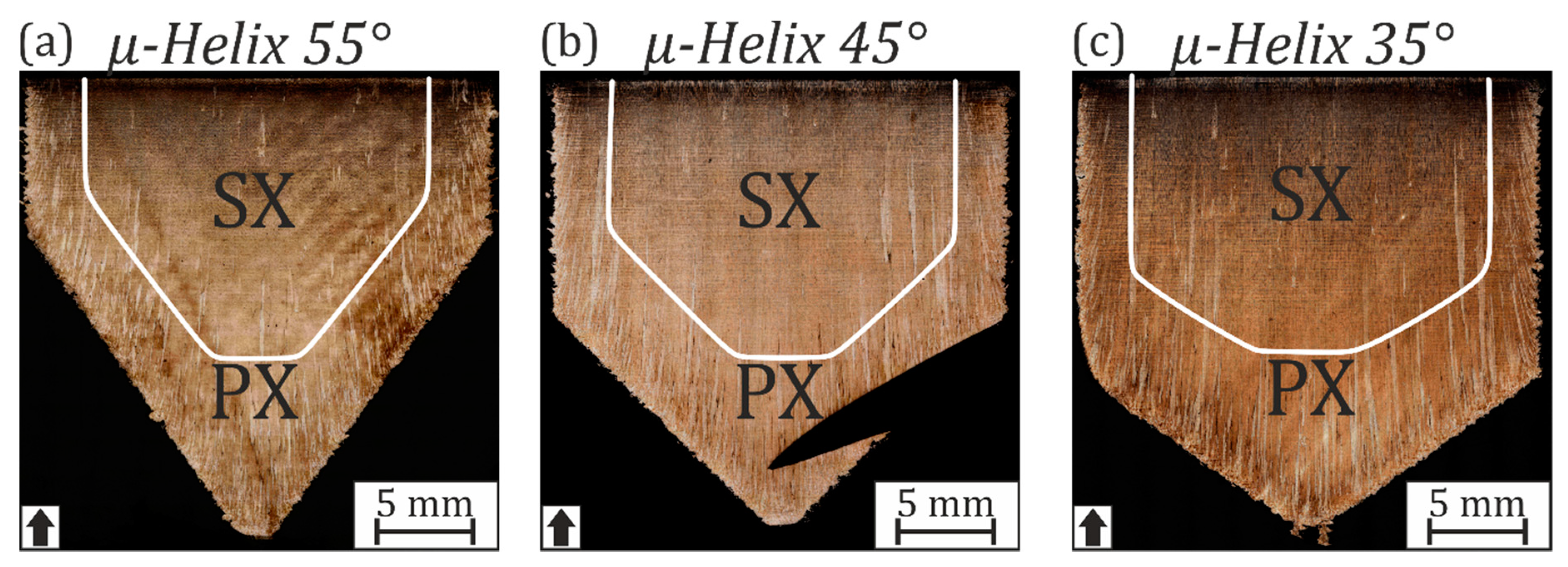
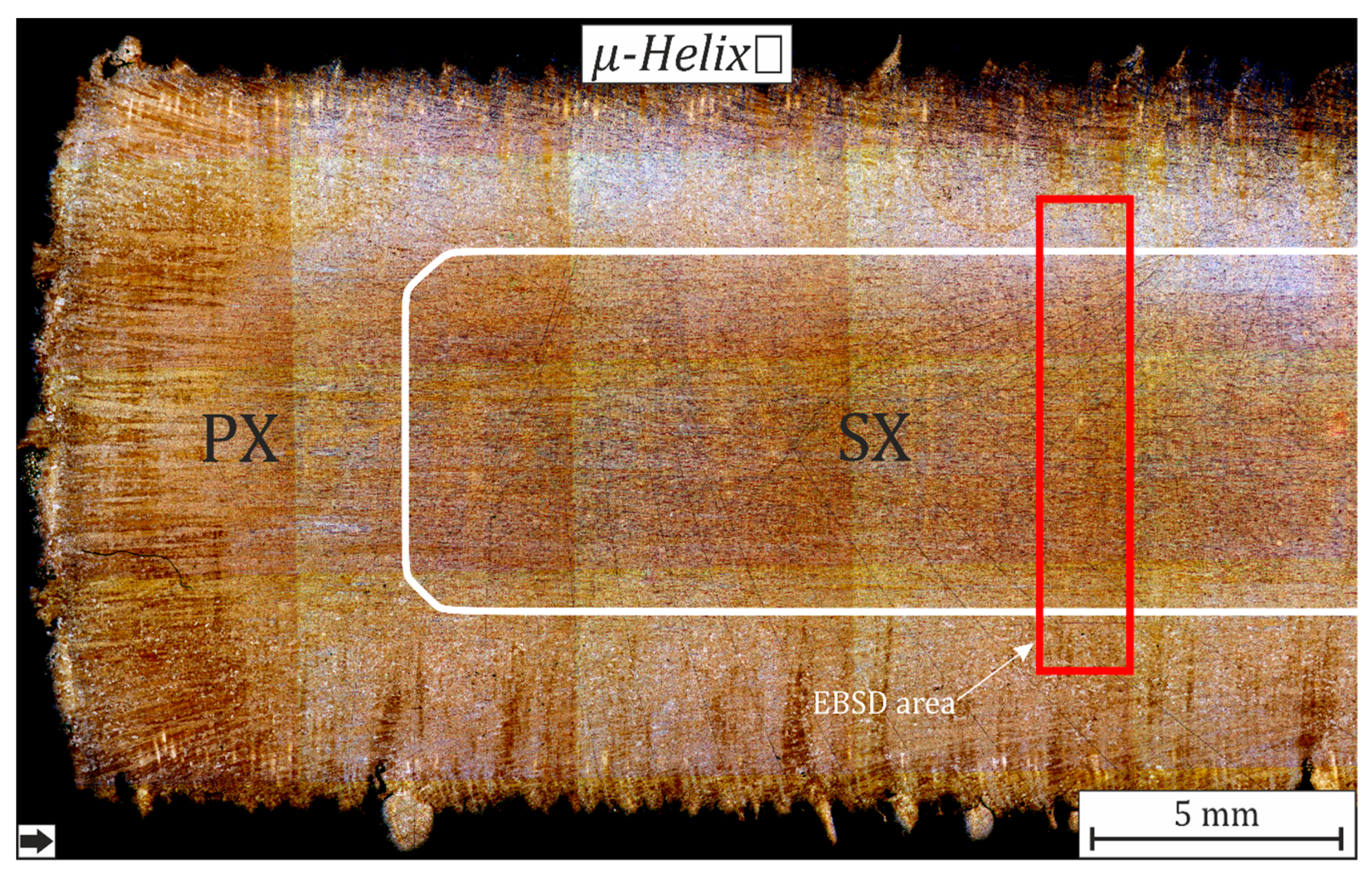
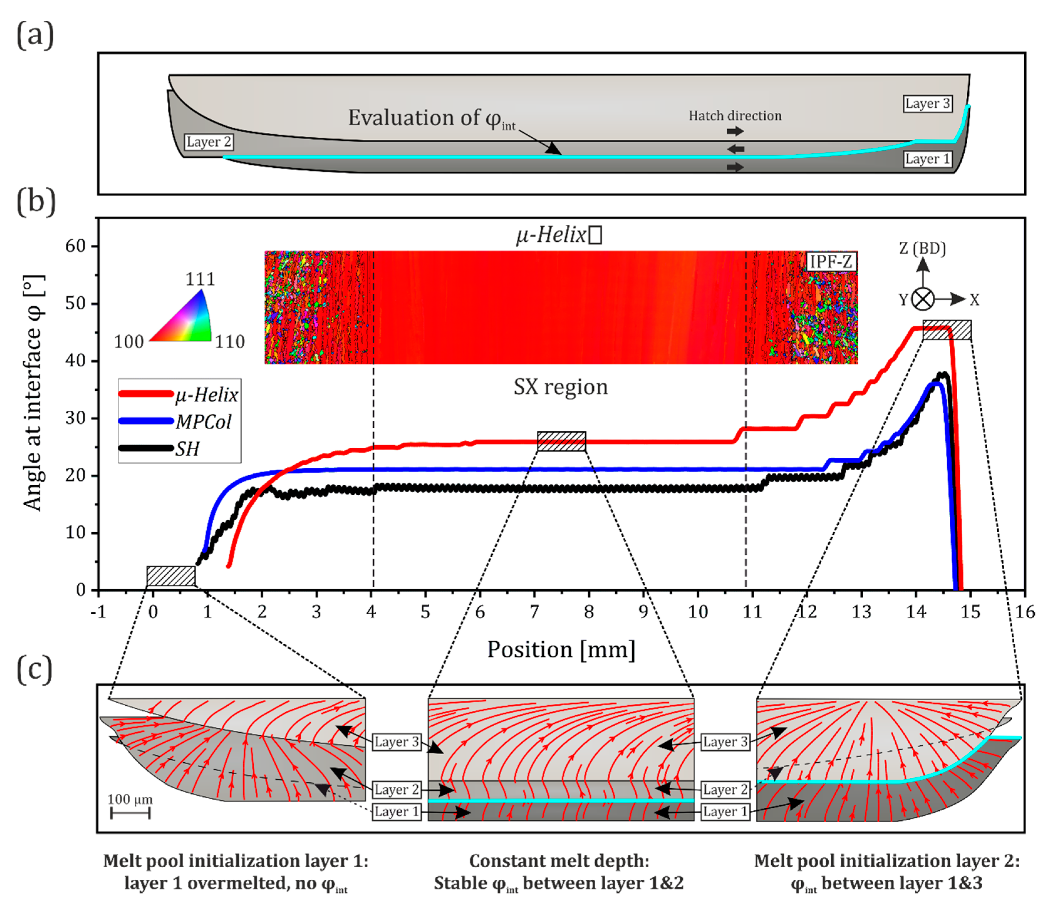
  • Standard hatching and multi passing yield columnar grains with a pronounced <100> fiber texture along the build direction. The novel µ-Helix parameter setting, a special variant of multi passing, allowed for the fabrication of technical single crystals (SXs), which were surrounded by a polycrystalline shell. Within the SX section, minor agglomerations of stray grains were still present. This was overcome in a second build job with improved temperature control, which resulted in high quality cuboid SX samples.
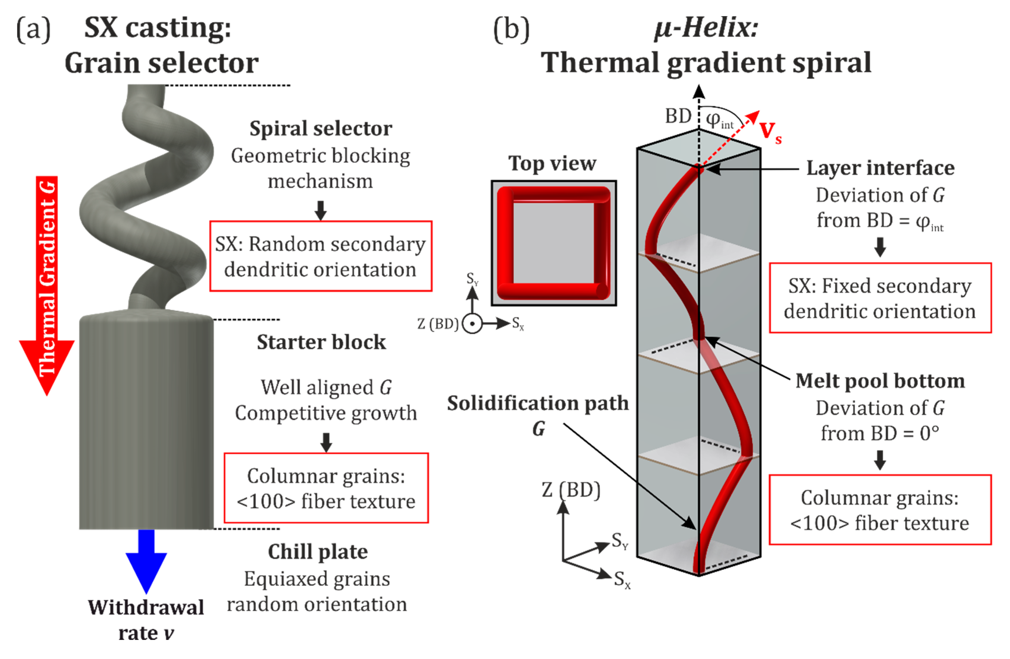
  • In contrast to investment casting, where the secondary orientation of single crystals produced by a spiral grain selector is random, SEBM leads to a defined and reproducible secondary orientation. All SXs show a primary orientation of <100> parallel to the build direction, and a secondary orientation of <110> along the scan vectors.
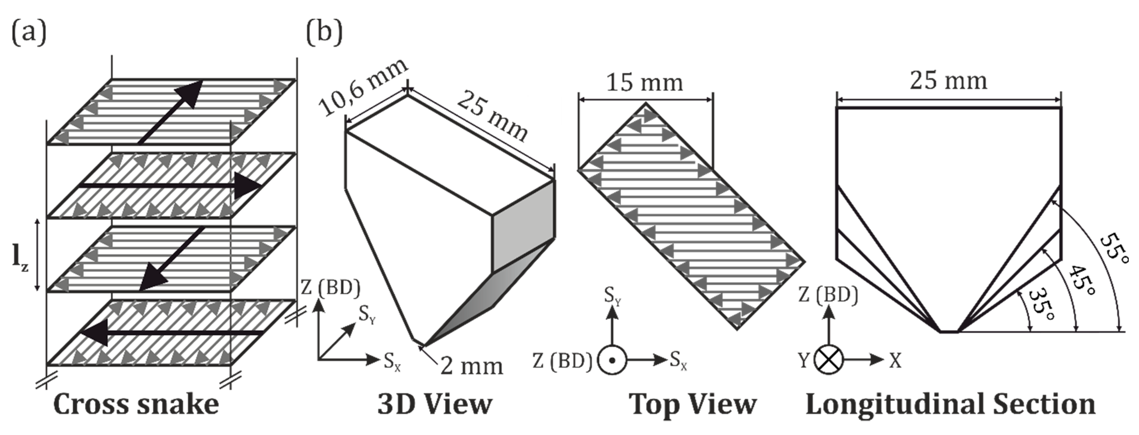
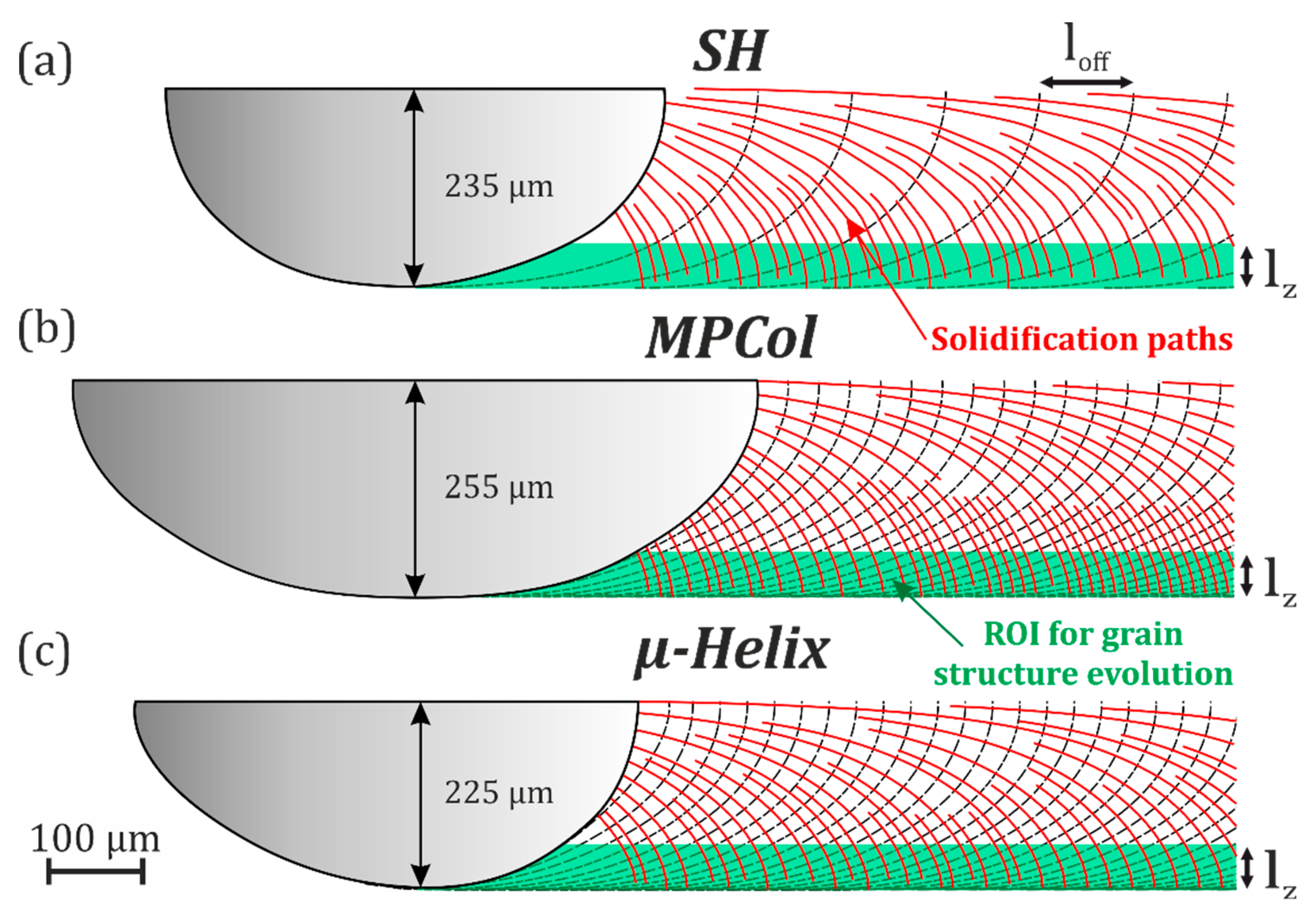
  • The aperture angle of the trapezoidal prisms determines the height where the SX region reaches its maximum width as new grain orientations emerge as long as the sample cross section still increases.
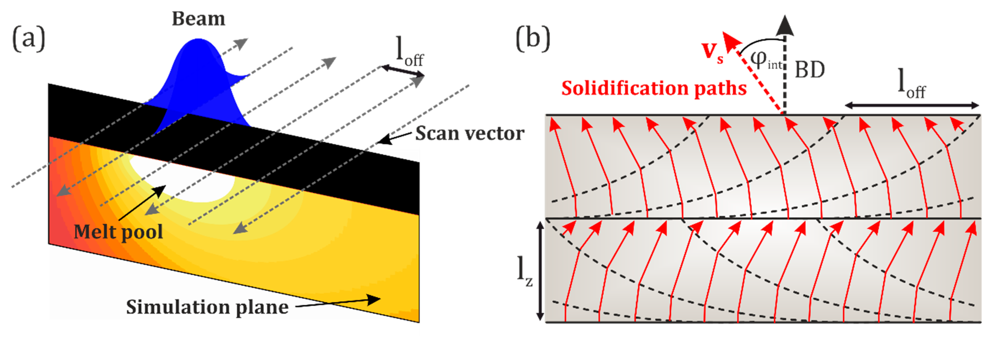
  • Numerical simulations using our in-house software suite S A M PLE 2 D revealed that the deviation of the thermal gradient G from the build direction, right at the interface between two layers, φint, correlates with the effectiveness of grain selection. The higher φint, the stronger the grain selection. The µ-Helix parameter setting forces the solidification paths along a µm-sized helix over the course of multiple layers.
  • The grain selection mechanisms leading to an SX are two-fold. As G deviates only slightly at the bottom of each melt pool, competitive growth between the grains based on their primary dendritic orientation is triggered, yielding a columnar grain structure. The increasing deviation of G from the BD closer to the layer interface leads to grain selection based on the secondary dendritic orientation. This mechanism is not yet fully understood and still under investigation.

Author Contributions

Conceptualization, M.R.G. and C.K.; methodology, M.R.G., A.M.R. and C.K.; software, A.M.R.; validation, M.R.G., A.M.R. and C.K.; formal analysis, M.R.G., A.M.R. and C.K.; investigation, M.R.G.; resources, C.K.; data curation, A.M.R.; writing—original draft preparation, M.R.G.; writing—review and editing, M.R.G. and C.K.; visualization, M.R.G., A.M.R. and C.K.; supervision, C.K.; project administration, C.K.; funding acquisition, C.K. All authors have read and agreed to the published version of the manuscript.

Funding

This research was funded by the Deutsche Forschungsgemeinschaft (DFG) through the Collaborative Research Center SFB/TR 103, Project B2.

Conflicts of Interest

The authors declare no conflicts of interest. The funders had no role in the design of the study; in the collection, analyses, or interpretation of data; in the writing of the manuscript, or in the decision to publish the results.

References

  1. Körner, C. Additive manufacturing of metallic components by selective electron beam melting—A review. Int. Mater. Rev. 2016, 61, 361–377. [Google Scholar] [CrossRef] [Green Version]
  2. Strondl, A.; Palm, M.; Gnauk, J.; Frommeyer, G. Microstructure and mechanical properties of nickel based superalloy IN718 produced by rapid prototyping with electron beam melting (EBM). Mater. Sci. Technol. 2011, 27, 876–883. [Google Scholar] [CrossRef]
  3. Helmer, H.E.; Hartmann, N.; Körner, C.; Singer, R.F. Relation Between Processing Strategy, Grain Structure and Mechanical Properties in Superalloy Inconel 718 Processed by Selective Electron Beam Melting. In Proceedings of the DDMC 2014, Fraunhofer Direct Digital Manufacturing Conference, Berlin, Germany, 12–13 March 2014. [Google Scholar]
  4. Sun, S.-H.; Koizumi, Y.; Saito, T.; Yamanaka, K.; Li, Y.-P.; Cui, Y.; Chiba, A. Electron beam additive manufacturing of Inconel 718 alloy rods: Impact of build direction on microstructure and high-temperature tensile properties. Addit. Manuf. 2018, 23, 457–470. [Google Scholar] [CrossRef]
  5. Strondl, A.; Fischer, R.; Frommeyer, G.; Schneider, A. Investigations of MX and γ′/γ″ precipitates in the nickel-based superalloy 718 produced by electron beam melting. Mater. Sci. Eng. A 2008, 480, 138–147. [Google Scholar] [CrossRef]
  6. Al-Bermani, S.S.; Blackmore, M.L.; Zhang, W.; Todd, I. The Origin of Microstructural Diversity, Texture, and Mechanical Properties in Electron Beam Melted Ti-6Al-4V. MMTA 2010, 41, 3422–3434. [Google Scholar] [CrossRef]
  7. Antonysamy, A.A.; Meyer, J.; Prangnell, P.B. Effect of build geometry on the β-grain structure and texture in additive manufacture of Ti6Al4V by selective electron beam melting. Mater. Charact. 2013, 84, 153–168. [Google Scholar] [CrossRef]
  8. Helmer, H.; Bauereiß, A.; Singer, R.F.; Körner, C. Grain structure evolution in Inconel 718 during selective electron beam melting. Mater. Sci. Eng. A 2016, 668, 180–187. [Google Scholar] [CrossRef]
  9. Raghavan, N.; Dehoff, R.; Pannala, S.; Simunovic, S.; Kirka, M.; Turner, J.; Carlson, N.; Babu, S.S. Numerical modeling of heat-transfer and the influence of process parameters on tailoring the grain morphology of IN718 in electron beam additive manufacturing. Acta Mater. 2016, 112, 303–314. [Google Scholar] [CrossRef] [Green Version]
  10. Kirka, M.M.; Lee, Y.; Greeley, D.A.; Okello, A.; Goin, M.J.; Pearce, M.T.; Dehoff, R.R. Strategy for Texture Management in Metals Additive Manufacturing. JOM 2017, 69, 523–531. [Google Scholar] [CrossRef] [Green Version]
  11. Ramsperger, M.; Carolin, K. Selective Electron Beam Melting Of The Single Crystalline Nickel-Base Superalloy Cmsx-4®: From Columnar Grains To A Single Crystal. In Superalloys 2016; John Wiley & Sons: Hoboken, NJ, USA, 2016. [Google Scholar]
  12. Chauvet, E.; Tassin, C.; Blandin, J.-J.; Dendievel, R.; Martin, G. Producing Ni-base superalloys single crystal by selective electron beam melting. Scr. Mater. 2018, 152, 15–19. [Google Scholar] [CrossRef]
  13. Mainprice, D.; Bachmann, F.; Hielscher, R.; Schaeben, H. Descriptive tools for the analysis of texture projects with large datasets using MTEX: Strength, symmetry and components. Geol. Soc. Lond. Spec. Publ. 2014, 409, SP409. [Google Scholar] [CrossRef]
  14. Markl, M.; Rausch, A.M.; Küng, V.E.; Körner, C. SAMPLE: A Software Suite to Predict Consolidation and Microstructure for Powder Bed Fusion Additive Manufacturing. Adv. Eng. Mater. 2019, 1901270. [Google Scholar] [CrossRef] [Green Version]
  15. Pottlacher, G.; Hosaeus, H.; Kaschnitz, E.; Seifter, A. Thermophysical properties of solid and liquid Inconel 718 Alloy *. Scand. J. Metall. 2002, 31, 161–168. [Google Scholar] [CrossRef]
  16. Mills, K.C. Recommended Values of Thermophysical Properties for Selected Commercial Alloys; Woodhead: Cambridge, UK, 2002. [Google Scholar]
  17. Mills, K.C.; Youssef, Y.M.; Li, Z.; Su, Y. Calculation of Thermophysical Properties of Ni-based Superalloys. ISIJ Int. 2006, 46, 623–632. [Google Scholar] [CrossRef] [Green Version]
  18. Walton, D.; Chalmers, B. The origin of the preferred orientation in the columnar zone of ingots. Trans. Metall. Soc. AIME 1959, 215, 447–457. [Google Scholar]
  19. Harald, E.H. Additive Fertigung durch Selektives Elektronenstrahlschmelzen der Nickelbasis Superlegierung IN718: Prozessfenster, Mikrostruktur und Mechanische Eigenschaften. Ph.D. Thesis, Friedrich-Alexander-Universität Erlangen-Nürnberg, Erlangen, Germany, 2017. [Google Scholar]
  20. Dehoff, R.R.; Kirka, M.M.; List, F.A.; Unocic, K.A.; Sames, W.J. Crystallographic texture engineering through novel melt strategies via electron beam melting: Inconel 718. Mater. Sci. Technol. 2015, 31, 939–944. [Google Scholar] [CrossRef]
  21. Koepf, J.A.; Gotterbarm, M.R.; Markl, M.; Körner, C. 3D multi-layer grain structure simulation of powder bed fusion additive manufacturing. Acta Materialia 2018, 152, 119–126. [Google Scholar] [CrossRef]
  22. Dai, H.J.; D’Souza, N.; Dong, H.B. Grain Selection in Spiral Selectors During Investment Casting of Single-Crystal Turbine Blades: Part I. Experimental Investigation. Metall. Mater. Trans. A 2011, 42, 3430–3438. [Google Scholar] [CrossRef]
  23. Dai, H.J.; Dong, H.B.; D’Souza, N.; Gebelin, J.-C.; Reed, R.C. Grain Selection in Spiral Selectors During Investment Casting of Single-Crystal Components: Part II. Numerical Modeling. Metall. Mater. Trans. A 2011, 42, 3439–3446. [Google Scholar] [CrossRef]
  24. Rausch, A.M.; Gotterbarm, M.R.; Markl, M.; Körner, C. Nucleation Mechanism in Powder Bed Fusion Additive Manufacturing; 2020; Manuscript in preparation. [Google Scholar]
Figure 1. (a) Schematic of the cross snake scan strategy used; (b) Schematic of the trapezoidal prism geometry used in the present study. The build direction (BD) Z and the scan vectors SX and SY are indicated. Note the rotation of the sample coordinates X and Y in the longitudinal sections by 45° with respect to SX and SY.
Metals 10 00313 g001
Figure 2. (a) Schematic of the simulation domain. The temperature field and the melt pool shape are shown. For convenience, the whole domain (width 15 mm) is not illustrated. The beam’s hatch pattern is schematically shown. (b) Schematic illustration of the solidification directions within overlapping melt pools. The maximum angle between thermal gradient G (proportional to the solidification velocity vs) and the BD, φint, is reached at the interface between two layers, while φint is about 0° at the bottom of the next layer.
Metals 10 00313 g002
Figure 3. Macro-etched longitudinal sections (ac) and corresponding detailed pictures (df) from trapezoidal prisms manufactured with different SEBM processing parameters and aperture angles of 35°. The build direction is indicated by the black arrows. The µ-Helix parameter setting allows the fabrication of technical single crystals (SXs). For convenience, the SX region (white), as well as the areas for the electron backscatter diffraction (EBSD) measurements are highlighted (red). SH—standard hatching; MPCol—multi passing.
Metals 10 00313 g003
Figure 4. Macro-etched longitudinal sections from trapezoidal prisms manufactured with the µ-Helix parameter setting. The build direction is indicated by the black arrows. The aperture angle of (a) 55°, (b) 45° and (c) 35° in the wedge section influences the overall shape of the SX region (white), but the SX selection height of about 9 mm remains constant.
Metals 10 00313 g004
Figure 5. Macro-etched longitudinal section of a cuboid sample manufactured with the µ-Helix parameter setting. The build direction is indicated by the black arrows. A high quality SX region is present in the center of the sample. For convenience, the SX region (white), as well as the areas for the EBSD measurements are highlighted (red).
Metals 10 00313 g005
Figure 6. Large area EBSD-IPF maps of trapezoidal prisms manufactured with different SEBM processing parameters: (a) SH, (b) MPCol, (c) µ-Helix. The build direction is indicated by the black arrows. Grain boundaries with a misorientation angle of > 10° are highlighted with black lines. The dashed lines indicate the region of interest for the pole figure of the µ-Helix sample.
Metals 10 00313 g006
Figure 7. (100) Orientation distribution function (ODF) of pole figures from the EBSD measurements of Figure 6 and Figure 8. The respective texture indices J O D F and hatching directions are given.
Metals 10 00313 g007
Figure 8. Large area EBSD-IPF maps of a cuboid sample manufactured with the µ-Helix parameter setting. The build direction is indicated by the black arrows. Grain boundaries with a misorientation angle of > 10° are highlighted with black lines. The dashed lines indicate the region of interest for the pole figures.
Metals 10 00313 g008
Figure 9. Numerical results from S A M PLE 2 D (Simulation of Additive Manufacturing on the Powder scale using a Laser or Electron beam). The dark grey areas represent the melt pools for (a) SH, (b) MPCol, (c) µ-Helix. The dashed lines indicate previous pools. Due to remelting in subsequent beam passes and layers, only a small region of interest (ROI) remains for grain structure development (highlighted in green). The red streamlines resemble the orientation of G, i.e., the solidification paths.
Metals 10 00313 g009
Figure 10. Analysis of the solidification conditions via S A M PLE 2 D . (a) Schematic showing an overlay of three simulated layers. The resulting location for the evaluation of φint is highlighted. (b) Deviation of the thermal gradient G from the BD at the interface between two layers φint, as a function of the position within the simulation domain. The plotted curves resemble moving averages of the original data for enhanced visibility. A section of the EBSD IPF-Z map of the cuboid µ-Helix sample is fit in for comparison. (c) Detailed results of the simulation of µ-Helix. The red streamlines resemble the orientation of G, i.e., the solidification paths.
Metals 10 00313 g010
Figure 11. Schematic illustration of different approaches to realize single crystals. (a) Physical spiral grain selector used within an investment casting mold, (b) µ-Helix selector during SEBM formed by the direction of the local thermal gradient G.
Metals 10 00313 g011
Table 1. Selective Electron Beam Melting (SEBM) processing parameters for trapezoid samples.
Parameter SettingScan StrategyScan Speed [m/s]Line Offset [µm]Beam Power [W]Build Temperature [°C]Layer Thickness [µm]
Standard hatching (SH)Cross snake310066095050
Multi passing (MPCol)Cross snake133085895050
Multi passing (µ-Helix)Cross snake73054695050
Table 2. Chemical composition (wt.%) of the IN718 powder used.
FeNiCrNbMoTiAlCoC
Bal.53.618.15.383.070.970.60.220.024
Table 3. Material parameters for IN718 used in S A M PLE 2 D [15,16,17]. The thermal conductivity in the solid and the liquid are linearly approximated with the temperature (T) in K.
ParameterValueUnit
Density7580Kgm−3
Dynamic Viscosity4.0 × 10−3Pas
Atomic Mass26.73u
Surface Tension1.73Nm−1
Solidus Temperature1528K
Liquidus Temperature1610K
Heat Capacity (solid)652JKg−1K−1
Heat Capacity (liquid)778JKg−1K1
Thermal Conductivity (solid)1.66 × 10⁻² T + 5.80 Wm−1K−1
Thermal Conductivity (liquid)1.35 × 10⁻² T + 5.15Wm−1K−1
Latent Heat of Fusion2.27∙105JK−1

