1. Introduction
Nanocrystalline materials, and in particular metals, whose grain sizes do not exceed 100 nm, have become attractive for use in various industries due to their specific physicochemical and mechanical properties. Several techniques are known for the synthesis of nanocrystalline materials in the form of thin films or coatings on various substrates: chemical vapor deposition (CVD), physical vapor deposition (PVD), electrochemical deposition (ED), electroless deposition (EL), etc. [
1]. Physical methods for deposition of thin films, such as sputtering or evaporation, are limited in terms of film thickness, intended for thin films of less than 1–2 µm [
2]. Unlike physical methods, there are no restrictions on the thickness of the film during the application of electrodeposition methods.
For application in Micro-Electromechanical Systems (MEMS) technologies, thin films and coatings must have good adhesion to the substrate, good corrosion resistance and good wear resistance, while maintaining satisfactory mechanical properties [
3,
4,
5,
6,
7]. In MEMS technologies, the processes of the formation of uniform and compact Cu films and coatings are applied in the production of inductive copper micro-coils for magnetic particles detection [
8], in combination with micro-machining techniques to obtain micro-gear [
9], for wiring on printed circuit boards (PCBs) and bottom-up filling or superfilling techniques for fabrication of Through Silicon Via (TSV) structures [
10]. In addition, copper coatings are used as sacrificial layers for the production of different laminar composite structures [
11]. Aside from MEMS technologies, various processes of Cu deposition also found a wide application in microelectronic packaging and interconnects [
12,
13].
For all the above-mentioned applications, good film quality at the micro- or nano-level is required, and electrodeposition processes are very suitable to reach it. In relation to the application of constant regimes of electrolysis, the improvement of the quality of Cu coatings, i.e., their morphological and structural characteristics, can be achieved by the application of electrodeposition at a periodically changing rate [
14,
15,
16], and the addition of specific substances known as additives to the electroplating baths [
17,
18,
19], or simply by the regulation of parameters of electrolysis including mixing of the electrolyte, finding of the optimal temperature for electrodeposition or balanced salt/acid contents when acidic baths are used [
20,
21].
One of the most important mechanical characteristics of metal films and coatings is microhardness, which is closely dependent on processing parameters used for their production [
22,
23]. Examining the mechanical response of a composite system constructed from substrate and film or coating on indentation and estimating the absolute film hardness independently from the substrate hardness include knowledge of parameters and phenomena such as type of the composite system [
24], applied load, duration of the applied load at indentation (dwell time) and indentation depth [
25,
26], thickness of the coatings [
27], elastic properties of the coatings [
28], indentation size effect (ISE) [
29,
30,
31,
32], interfacial adhesion [
33,
34], etc. A large number of mathematical composite models have been developed so far to determine the “true” or absolute hardness of the film [
27,
32,
33,
34,
35,
36].
In this study, morphological, structural and mechanical characteristics of Cu coatings electrodeposited on Si(111) substrate by the pulsating current (PC) regime were examined. This was done with the aim to define working conditions enabling the formation of uniform and compact coatings of high microhardness. For that purpose, parameters of the PC regime, such as the current density amplitude and frequency (pause duration), were analyzed. The thickness of the coatings was also examined. The composite hardness model of Chicot–Lesage (C–L) was chosen and applied to experimental data in order to analyze the composite systems made [
27,
35,
36]. The basis of the theory of the composite hardness model according to Chicot–Lesage (C–L) is given in
Appendix A.
4. Discussion
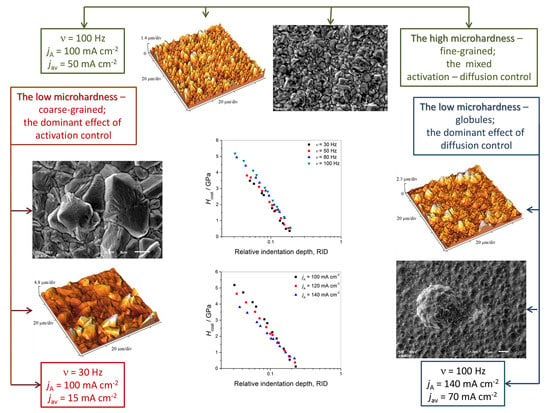
It is clear from the above consideration that the highest value of copper coating microhardness was achieved with a
jA of 100 mA·cm
−2 at 100 Hz, i.e., and with a
jav of 50 mA·cm
−2 (
Figure 2g,h). This coating was fine-grained and had the smallest roughness. High coating microhardness values were also achieved at a frequency of 80 Hz (
Figure 2e,f), as well as with the current density amplitude
jA of 120 mA·cm
−2 (
Figure 3a,b). These coatings also have fine-grained structure and their roughness was slightly higher than that obtained with a
jA of 100 mA·cm
−2 at 100 Hz.
For the lowest frequency value of 30 Hz, the obtained coating was coarse-grained with large relatively well-defined grains (
Figure 2a,b). The roughness of this coating was considerably higher than those observed at 80 and 100 Hz, as well as with a
jA of 120 mA·cm
−2. The direct consequence is the lower coating microhardness value. Similar results to those for 30 Hz were obtained when the 50 Hz frequency was applied (
Figure 2c,d). Applying the current density amplitude of 140 mA·cm
−2, a rough structure with globules was obtained (
Figure 3c,d), and as a result of this, the decrease of microhardness of this Cu coating was observed.
All the above-mentioned surface morphologies had a thickness of 40 μm. In coatings of 10 and 20 μm thickness, a contribution of the substrate hardness to the composite hardness was significant. With an increasing thickness of the coatings, the roughness of coatings increased (
Figure 8), resulting in a decrease of composite hardness and coating microhardness for the coating electrodeposited with a thickness of 60 μm relative to that of 40 μm.
Due to the strong dependence of morphology and structure of Cu coatings on the microhardness, optimization of the process of the formation of Cu coatings with a compact and uniform structure on Si(111) by the PC regime was done and discussed as follows.
Table 6 shows summarized values of overpotential amplitude (
ηA) response obtained with analyzed parameters of the PC regime during electrodeposition processes.
In the PC regimes, overpotential amplitude responses consist of the activation and diffusion parts, where a contribution of the activation part of the overpotential depends on the pause-to-pulse ratio and increases with it, i.e., a contribution of the activation part increases with an increase of pause duration and a decrease of frequency [
47]. The set of equations explaining it is given in
Appendix C.
Regarding the fact the that formation of large well-defined grains is a characteristic of the activation control of the electrodeposition [
38,
43], it is clear that Cu coatings obtained with a
p of 5.66 and 3 (30 and 50 Hz;
Figure 2a–d) are formed under conditions of the dominant activation control of the electrodeposition. Of course, a contribution of the activation control to the overall control was larger with an applied frequency of 30 Hz (
Figure 2a,b) than with 50 Hz (
Figure 2c,d). The high contribution of the activation control at 30 Hz is confirmed by an overpotential amplitude response at this frequency of 99−135 mV (
Table 6), which corresponds to the end of the activation control and to the beginning of the mixed activation–diffusion control of the electrodeposition (
Figure 1).
The formation of globules with an amplitude of 140 mA·cm
−2 (
Figure 3c) clearly indicates that the contribution of diffusion becomes dominant in the overall control of the electrodeposition process. This is confirmed by an overpotential amplitude response of 380–500 mV corresponding to the end of the mixed activation–diffusion control (
Figure 1).
Hence, optimum conditions for the formation of compact and uniform films of satisfactory microhardness corresponds to the range of overpotential in the mixed activation–diffusion control between the end of the effect of the activation control and the beginning of the dominant effect of diffusion control. For these working conditions, the optimum conditions are in the range of overpotentials between 200 and 400 mV (denoted by vertical dash lines in
Figure 1), and they can be achieved in different ways by appropriate selection of parameters of the PC regimes. Of course, one challenge in the future will be to extend this overpotential range.
Aside from the strong effect on the morphology of the Cu coatings, the applied parameters of PC regimes also had a strong effect on the structure of the coatings leading to a change of preferred orientation from the strong (220) to the strong (111), that can be explained in the following way.
For the FCC crystal lattice of Cu, the values of surface energy of crystal planes follow the trend:
γ111 <
γ100 <
γ311 <
γ110 [
48,
49]. As a result of different surface energy values, rate of electrodeposition is different on crystal planes, following the opposite trend from that for surface energy values [
50]. The (100), (110) and (311) crystal planes are situated to the group of fast-growing planes, while the (111) plane belongs to the group of slow-growing crystal planes [
51]. It means that during the electrodeposition process, the fast-growing (100), (110) and (311) planes disappear firstly, while the slow-growing (111) plane survives.
The average current density of 15 mA·cm−2 is too low to cause the disappearance of the fast-growing (220) plane, and the coarse Cu coating with large grains obtained at this average current density (i.e., at 30 Hz) showed the strong (220) preferred orientation. Intensification of the electrodeposition process through an increase of jav from 15 to 25 mA·cm−2 led to faster disappearing of Cu crystallites oriented in the (220) plane, and an increase of the ratios of Cu crystallites oriented in the next (311) plane. As a result of this, the Cu coating obtained at a jav of 25 mA·cm−2 (i.e., at 50 Hz) showed a smaller degree of (220) preferred orientation than that obtained at 30 Hz. The further increase of the average current density from 40 mA cm−2 (80 Hz) and 50 mA·cm−2 (100 Hz) to 60·mA·cm−2 (jA = 120 mA·m−2) led to the formation of Cu coatings with crystallites preferentially oriented in the (311) and (111) planes. It is necessary to note that the ratio of Cu crystallites oriented in the fast-growing (311) plane decreased, while the ratio of Cu crystallites oriented in the slow-growing (111) plane increased by increasing the average current density from 40 to 60 mA cm−2. Finally, the Cu coating obtained at the average current density of 70 mA·cm−2 at which diffusion became the dominant process possessed the strong (111) preferred orientation.
Composite hardness values,
Hc, were calculated from the experimentally measured indentation diagonals according to Equation (1) from
Appendix A. The increase of
Hc for the RID < 0.1 can be explained by strengthening of the coatings by deformation [
35,
36,
52].
The obtained results are in accordance with the Hall−Petch effect [
53], predicting the linear dependence of the hardness of the deposits on the reciprocal square root of grain size [
54,
55]. Namely, it is well known that an increase in the current density of electrodeposition leads to a decrease of grain size causing an increase in the hardness of deposits [
53]. This linear dependence is valid up to some value of grain size corresponding to the certain current density, after which the value of the hardness of the deposit begins to decrease. The decrease of hardness after maximum value, i.e., the transition from grain-size strengthening to grain-size softening can be attributed to a change in the triple junction (i.e., intersection of three or more grain boundaries) volume fraction [
53]. In our case, it is clear that the increase of hardness with the decrease of grain size can be attributed to the grain-size strengthening effect achieved in the mixed activation–diffusion control, while the grain size softening effect corresponds to the beginning of the dominant diffusion control of electrodeposition when globules forms.
According to the C–L model, it is possible to calculate the hardness of the coating only from the microhardness results (diagonal of the indent), because the values obtained for the coating hardness are influenced by the applied load. How the coating hardness changes according to this model will depend not only on the type of composite system, but also on the hardness of the coating and the substrate and the ratio of their hardness values. Due to the observation of the variation in hardness of the coating with RID, we applied the model to all samples. According to Equation (7) (
Appendix A), the largest effects on the coating hardness have coefficients
A,
B, and
C, which are dependent on parameter
f. This parameter is a function of
δ/
d, and the C–L model gives the most reliable results for the
δ/
d ratios of about 1 [
56,
57]. In our case, this condition is fulfilled for coating thicknesses of 10 and 20 µm in the whole range of examined loads. For the coating thickness of 40 µm, this condition is fulfilled in the RID range between 0.1 and 1 for the composite hardness and to a greater extent for the coating hardness. Regarding the coating thickness of 60 µm, the
δ/
d ratio is considerably larger than 1, causing noticeably larger values for the composite and the coating hardness. It is worth noting that such high values of coating hardness have been reported already for the Cu coatings obtained by pulse electrodeposition [
52].
The discrepancy between the composite hardness and the calculated coating hardness can be explained as follows: the composite hardness is determined from Equation (1), while the coating hardness is determined from Equation (7) (both equations from
Appendix A). As already mentioned, the main parameter affecting the coating hardness is
δ/
d, where a contribution of this parameter in the calculation of the coating hardness increases by increasing the thickness of the coating. As a result of this, the difference between the composite and the coating hardness increases by increasing the coating thickness, causing a limitation in the application of the C–L model for the thicker coatings. Of course, morphological characteristics of coatings, such as shape and size of grains, roughness of the coatings, as well as substrate type, also affect the final values of the composite and the coating hardness.
Anyway, the high microhardness showed the Cu coatings with Cu crystallites predominantly oriented in the (111) plane, which is the closest-packed crystal plane of the FCC lattice. According to our opinion, similar to mirror bright Cu coatings [
58], the (111) plane is not crucial for the enhanced microhardness of coatings, but it plays a significant role in this mechanical characteristic of Cu coatings.

 ,
, 


