Analytical Model to Calculate the Grain Size of Bulk Material Based on Its Electrical Resistance


Abstract
:1. Introduction
2. Materials and Methods
- 2.0 mm → 1.7 mm → 1.5 mm →1.3 mm → 1.1 mm → 0.9 mm → 0.7 mm
- 2.0 mm → 1.5 mm → 1.3 mm → 1.1 mm → 0.9 mm → 0.7 mm → 0.5 mm
- 2.0 mm → 1.9 mm → 1.4 mm → 0.8 mm
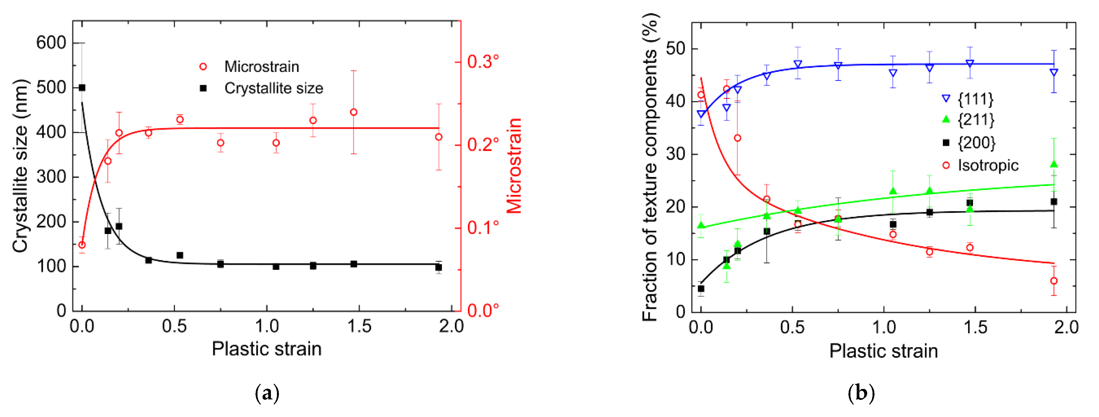
3. Results
- The current is not passing through high-angle grain boundaries that are aligned parallel to the direction along which the current is flowing.
- All grains are identical in regards to shape and size (i.e., homogenous sample).
- The density and distribution of low-angle grain boundaries are uniform in the grains across the relevant volume.
- The grains are aligned in rows or can be considered aligned by theoretical relocation of the grains.
- Grain boundaries within a row (including both high- and low-angle grain boundaries) of grains are not explicitly considered. They only contribute to an offset of the measured resistance.
- The parameter N (see below) is constant for samples produced by a similar process (e.g., rolling).
- The electrical resistivity ρ is independent of the grain size in the considered grain-size range.
3.1. Electrical Resistance of Cylindrical Grains along the Cylinder Axis
3.2. Electrical Resistance of Cylindrical Grains Perpendicular to the Cylinder Axis
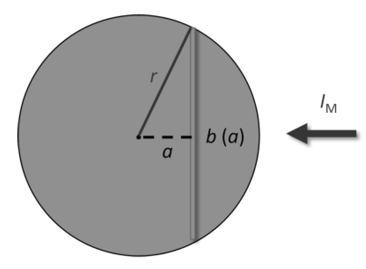
3.3. Electrical Resistance of Spherical Grains
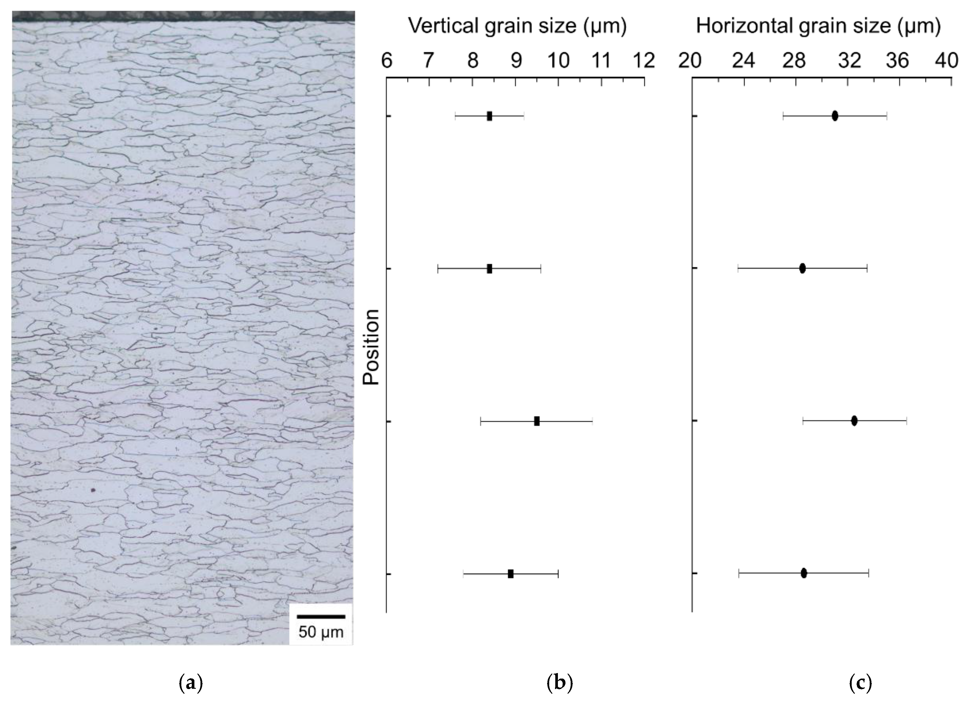
3.4. Microstructural Investigations of Rolled Sheets
4. Discussion
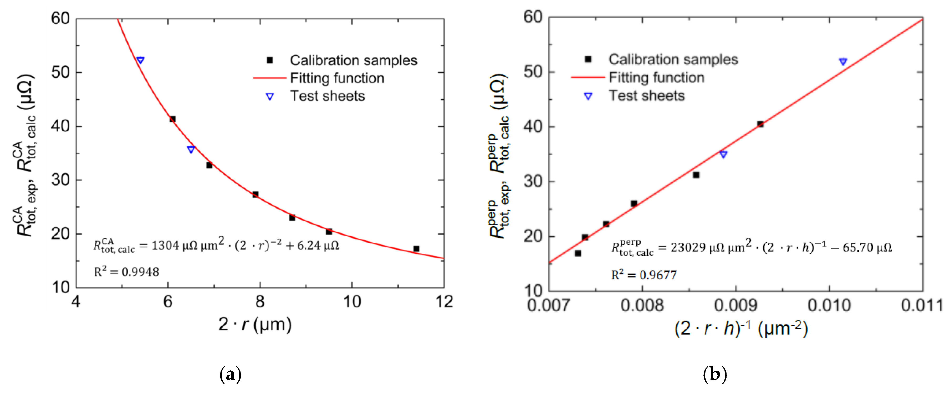
- Determination of the relevant grain sizes (r and h) of at least four to five calibration samples;
- Measurement of the electrical resistance along and perpendicular to the grain (cylinder) axis for these calibration samples;
- Fitting of the Equations (3) and (6) as shown in Figure 5a,b respectively. The fits do determine and fix N for the subsequent steps;
- Measurement of the electrical resistance along and perpendicular to the grain axis for samples with unknown grain sizes;
- By using the fitting function (along the grain axis), r can be determined;
- By using the fitting function (perpendicular to the grain axis) and r (step 5.), h can be calculated.
- Grain-size distributions cannot be determined. If a wide grain-size distribution is present, an average will be calculated that inaccurately describes the microstructure. In particular, bimodal grain-size distributions with very small and very large grains will cause the results to be inaccurate;
- The grain shape and orientation must be known;
- The grains in the sample can only be approximated by the idealized grain shape of a cylinder or sphere. Thus, the size of an equivalent cylinder or sphere will be determined when using the model;
- Depth gradients of the grain sizes or shapes cannot be analyzed. When measuring non-homogeneous samples, an average grain size will be determined, but due to the proportionality of the resistance to r−2, smaller grains will be stronger weighted;
- If the microstrain, i.e., the dislocation density, differs significantly across the sample, local differences in the specific resistance of the grains occur. Thus, the average specific resistance would differ from the assumed value in Equations (3), (6) and (9), which causes the calculated grain sizes to be shifted systematically. However, this effect is considered to be smaller than differences in the grain size because the equations only depend on the specific resistance linearly, and the relative change in the specific resistance of the grains is expected to be small.
5. Conclusions
Author Contributions
Funding
Institutional Review Board Statement
Informed Consent Statement
Data Availability Statement
Acknowledgments
Conflicts of Interest
References
- Turnbull, A.; De Los Rios, E.R. The Effect of Grain Size on the Fatigue of commercially pure Aluminium. Fatigue Fract. Eng. Mater. Struct. 1995, 18, 1455–1467. [Google Scholar] [CrossRef]
- Ralston, K.D.; Birbilis, N.; Davies, C.H.J. Revealing the relationship between grain size and corrosion rate of metals. Scr. Mater. 2010, 63, 1201–1204. [Google Scholar] [CrossRef]
- Mayadas, A.F.; Shatzkes, M. Electrical-Resistivity Model for Polycrystalline Films: The Case of Arbitrary Reflection at External Surfaces. Phys. Rev. B 1970, 1, 1382–1389. [Google Scholar] [CrossRef]
- Tellier, C.R. Size and Grain-Boundary Effects in the Electrical Conductivity of Thin Monocrystalline Films. Electrocompon. Sci. Technol. 1978, 5, 127–131. [Google Scholar] [CrossRef]
- Bedda, M.; Messaadi, S.; Pichard, C.R.; Tosser, A.J. Analytical expression for the total electrical conductivity of unannealed and annealed metal films. J. Mater. Sci. 1986, 21, 2643–2647. [Google Scholar] [CrossRef]
- Luo, W.; Zhu, L.-L.; Zheng, X.-J. Grain Size Effect on Electrical Conductivity and Giant Magnetoresistance of Bulk Magnetic Polycrystals. Chin. Phys. Lett. 2009, 26, 117502. [Google Scholar] [CrossRef]
- Durkan, C.; Welland, M.E. Size effects in the electrical resistivity of polycrystalline nanowires. Phys. Rev. B 2000, 61, 14215–14218. [Google Scholar] [CrossRef]
- Mannan, K.M.; Karim, K.R. Grain boundary contribution to the electrical conductivity of polycrystalline Cu films. J. Phys. F Met. Phys. 1975, 5, 1687–1693. [Google Scholar] [CrossRef]
- Lim, J.W.; Isshiki, M. Electrical resistivity of Cu films deposited by ion beam deposition: Effects of grain size, impurities, and morphological defect. J. Appl. Phys. 2006, 99, 094909. [Google Scholar] [CrossRef]
- Plombon, J.J.; Andideh, E.; Dubin, V.M.; Maiz, J. Influence of phonon, geometry, impurity, and grain size on Copper line resistivity. Appl. Phys. Lett. 2006, 89, 113124. [Google Scholar] [CrossRef]
- Kumar, A.; Singh, D.; Kaur, D. Grain size effect on structural, electrical and mechanical properties of NiTi thin films deposited by magnetron co-sputtering. Surf. Coat. Technol. 2009, 203, 1596–1603. [Google Scholar] [CrossRef]
- Day, M.E.; Delfino, M.; Fair, J.A.; Tsai, W. Correlation of electrical resistivity and grain size in sputtered titanium films. Thin Solid Film. 1995, 254, 285–290. [Google Scholar] [CrossRef]
- Moriyama, M.; Kawazoe, T.; Tanaka, M.; Murakamia, M. Correlation between microstructure and barrier properties of TiN thin films used Cu interconnects. Thin Solid Film. 2002, 416, 136–144. [Google Scholar] [CrossRef]
- Learn, A.J.; Foster, D.W. Resistivity, grain size, and impurity effects in chemically vapor-deposited tungsten films. J. Appl. Phys. 1985, 58, 2001–2007. [Google Scholar] [CrossRef]
- Zeng, H.; Wu, Y.; Zhang, J.; Kuang, C.; Yue, M.; Zhou, S. Grain size-dependent electrical resistivity of bulk nanocrystalline Gd metals. Prog. Nat. Sci. Mater. Int. 2013, 1, 18–22. [Google Scholar] [CrossRef] [Green Version]
- Santos, T.G.; Miranda, R.M.; Vilaça, P.; Teixeira, J.P. Modification of electrical conductivity by friction stir processing of aluminum alloys. Int. J. Adv. Manuf. Technol. 2011, 57, 511–519. [Google Scholar] [CrossRef]
- Metan, V.; Eigenfeld, K. Controlling mechanical and physical properties of Al-Si alloys by controlling grain size through grain refinement and electromagnetic stirring. Eur. Phys. J. Spéc. Top. 2013, 220, 139–150. [Google Scholar] [CrossRef]
- Barghout, J.Y.; Lorimer, G.W.; Pilkington, R.; Prangnell, P.B. The Effects of Second Phase Particles, Dislocation Density and Grain Boundaries on the Electrical Conductivity of Aluminium Alloys. Mater. Sci. Forum 1996, 217–222, 975–980. [Google Scholar] [CrossRef]
- Abbas, S.F.; Seo, S.-J.; Park, K.-T.; Kim, B.S.; Kim, T.-S. Effect of grain size on the electrical conductivity of copper–iron alloys. J. Alloys Compd. 2017, 720, 8–16. [Google Scholar] [CrossRef]
- Mehner, T.; Bauer, A.; Awiszus, B.; Lampke, T. Macromechanical finite-element simulations for predicting microstructures by experimental calibration. IOP Conf. Ser. Mater. Sci. Eng. 2017, 181, 12036. [Google Scholar] [CrossRef] [Green Version]


| q | |
|---|---|
| 0.70 | 0.8673 |
| 0.75 | 0.9730 |
| 0.80 | 1.0986 |
| 0.85 | 1.2562 |
| 0.90 | 1.4722 |
| 0.95 | 1.8318 |
| ds/mm | φ [20] | 2·r/µm | h/µm | ||
|---|---|---|---|---|---|
| with 95% Confidence Intervals | |||||
| 2.0 | 0.000 | 11.4 | 24.0 | 17.25 ± 0.14 | 16.93 ± 0.15 |
| 1.5 | 0.344 | 9.5 | 28.5 | 20.45 ± 0.10 | 19.84 ± 0.10 |
| 1.3 | 0.514 | 8.7 | 30.2 | 23.03 ± 0.15 | 22.27 ± 0.10 |
| 1.1 | 0.749 | 7.9 | 32.0 | 27.33 ± 0.13 | 26.00 ± 0.11 |
| 0.9 | 1.064 | 6.9 | 33.8 | 32.78 ± 0.20 | 31.24 ± 0.20 |
| 0.7 | 1.459 | 6.1 | 35.4 | 41.38 ± 0.13 | 40.50 ± 0.27 |
| Test sheets | |||||
| 0.8 | 1.251 | 6.5 | 34.7 | 35.81 ± 0.21 | 35.09 ± 0.17 |
| 0.5 | 1.933 | 5.4 | 36.5 | 52.40 ± 0.26 | 52.00 ± 0.16 |
Publisher’s Note: MDPI stays neutral with regard to jurisdictional claims in published maps and institutional affiliations. |
© 2020 by the authors. Licensee MDPI, Basel, Switzerland. This article is an open access article distributed under the terms and conditions of the Creative Commons Attribution (CC BY) license (http://creativecommons.org/licenses/by/4.0/).
Share and Cite
Mehner, T.; Uland, M.; Lampke, T. Analytical Model to Calculate the Grain Size of Bulk Material Based on Its Electrical Resistance. Metals 2021, 11, 21. https://doi.org/10.3390/met11010021
Mehner T, Uland M, Lampke T. Analytical Model to Calculate the Grain Size of Bulk Material Based on Its Electrical Resistance. Metals. 2021; 11(1):21. https://doi.org/10.3390/met11010021
Chicago/Turabian StyleMehner, Thomas, Morgan Uland, and Thomas Lampke. 2021. "Analytical Model to Calculate the Grain Size of Bulk Material Based on Its Electrical Resistance" Metals 11, no. 1: 21. https://doi.org/10.3390/met11010021
APA StyleMehner, T., Uland, M., & Lampke, T. (2021). Analytical Model to Calculate the Grain Size of Bulk Material Based on Its Electrical Resistance. Metals, 11(1), 21. https://doi.org/10.3390/met11010021