Article

Numerical Analysis of the Welding Behaviors in Micro-Copper Bumps

1
Department of Mechanical and Electro-Mechanical Engineering, National Sun Yat-sen University, Kaohsiung 80424, Taiwan
2
Department of Materials Science and Engineering, I-Shou University, Kaohsiung 84001, Taiwan
3
Department of Fragrance and Cosmetic Science, College of Pharmacy, Kaohsiung Medical University, 100 Shi-Chuan 1st Road, Kaohsiung 80708, Taiwan
*
Author to whom correspondence should be addressed.
Metals 2021, 11(3), 460; https://doi.org/10.3390/met11030460
Submission received: 29 January 2021 / Revised: 7 March 2021 / Accepted: 9 March 2021 / Published: 11 March 2021
(This article belongs to the Special Issue Numerical Simulation of Metals Welding Process)

Abstract

:
In this study, three-dimensional simulations of the ultrasonic vibration bonding process of micro-copper blocks were conducted using the finite element method. We analyzed the effects of ultrasonic vibration frequency on the stress field, strain field, and temperature field at the copper bump joint surface. The results showed that the bonding process is successfully simulated at room temperature. The stress curve of the bonding process could be divided into three stages: stress rising stage, stress falling stage, and stress stabilization stage. Moreover, it was found that the end of the curve exhibited characteristics of a solid solution phase at higher frequencies. It is hypothesized that the high-density dislocations formed at this stage may result in conveyance channels that facilitate the atomic diffusion at the contact surface. The simulation results indicated that copper micro-bump bonding occurs at an ultrasonic frequency of 50 kHz or higher.

1. Introduction

Modern science and technology are booming, and the development of semiconductors has progressed from two-dimensional integrated circuits (2D IC) to three-dimensional integrated circuits (3D IC). Manufacturers worldwide are hoping to build more modules on a single chip to achieve even higher integration density. The high integration density translates into a reduction of the total semiconductor and shortening of the internal circuit transmission path, which can accelerate the transmission of information. The increased efficiency and reduction in energy consumption is anticipated to further postpone the claim that the Moore’s law has reached its limit [1,2].
To achieve the above-mentioned goals, semiconductor manufacturers have proposed some key technologies in recent years, which can be divided into two categories: through silicon via (TSV) and micro-bump bonding technologies. It is noted, however, that despite the recent progresses driven by the increasing demands of converting from 2D to 3D IC, there are still plenty of challenges and opportunities requiring tremendous research and development in improving the reliability of vertical connections. In addition to intermetallic compound (IMC) formation, issues such as joule heating, harsh temperature gradients and associated thermo-migration, electro-migration, as well as stress-migration still must be addressed [3,4]. The key feature of the TSV technology is the formation of a vertical channel inside the silicon substrate, which is filled with a selected metal [5]. On the other hand, the bonding technology establishes junctions between wafers by using metal bonding bumps. Both technologies have been demonstrated to be capable of realizing 3D IC by forming a stack of wafers with built-in transistors and devices. Direct copper–copper bonding without solders has been considered as a promising technology to address the challenges of solder bonding owing to its excellent conductivity and high electro-migration resistance. As mentioned above, the two primary paths for 3D integration are for bonding copper onto copper bumps and bonding TSVs onto bumps. Both require high pressure and elevated temperatures to achieve good bonds.
Previously, it was successfully demonstrated that thermal compression bonding (TCB) temperature and time could be reduced to below 573 K and 900 s, respectively, and still achieve 80% electrical yield [6]. Normally, the dies with flattened bumps are used to perform copper–copper direct bonding via a thermal compression bonding (TCB) process, which often needs high bonding temperature and pressure and a long bonding time. Consequently, most of the challenges encountered in copper–copper bonding is bump co-planarity, surface roughness, thermal budget, and interface bonding quality. Moreover, in order to obtain successful TCB, factors such as the materials to be used and the required joining area also have to be considered. Overcoming the yield strength of copper for triggering plastic deformation in copper–copper bonding often requires a substantial compressive force with T > 573 K. In particular, for a fine-pitch high-density array of bumps, a massive amount of force is needed to achieve the necessary area of metal for bonding [6,7,8]. Alternatively, an approach for fabricating face-centered cubic (FCC) solid-solution joints without formation of intermetallic compounds was proposed by using a trace amount of gallium (Ga) and nickel (Ni) under-bump-metallurgy (UBM) for the reactive diffusion bonding at 573 K [9]. For instance, the effect of bonding force on bonding strength on the thermosonic flip chip bonding of a copper pillar with a tin cap was investigated [10]. An average bonding strength of approximately 84.8 MPa was obtained in 2 s under an optimal bonding force of 0.11 N per 40 μm pillar bump with a substrate temperature of 473 K. By increasing the temperature and time of the TCB process, the copper pillar solder joint with intermetallic compound (IMC) as the main body was obtained [11]. Recently, ultrasonic metal welding (USMW) has emerged as a prominent technology for bonding non-ferrous metals without utilizing filler materials [12]. In USMW, the imperious mechanism is the solid solution bonding enabled by plastic deformation and the slip caused by narrowly enforced high-frequency ultrasonic acoustic mechanical oscillations. Since the temperature developed in the USMW is around 30–80% of the melting point of the workpieces and the process is completed in the order of seconds, it is expected that the chemical properties of the workpieces could be minimally influenced. Additionally, with the reduction in stacking size and specific harsh environments required, the join process has become even more challenging. To meet part of these additional challenges, Watanabe and Asano [13] proposed a cone-bump process in combination with ultrasonic bonding that enabled room-temperature copper-copper bonding with base diameter of approximately 10 μm in ambient air. Die share tests revealed that the bonding strength obtained from this process was comparable to that bonded at 423 K [14].
To address the thermal reliability issues, studies have been conducted to improve the bonding process, allowing for a reduction in the process temperature and/or changing the process environment toward cost reduction and reliability improvement. Reducing the processing temperature, however, often requires more complicated extreme environmental conditions and/or special treatment with subsequent annealing steps to prepare the bonding surfaces and, thus, can be cost-demanding. For instance, a couples-polishing activation bonding process using ultrasonic vibration to produce a friction effect and make the contact interface has been proposed for making copper bonding at contacts [15,16,17]. One of the innovated technologies applied to bond nonwoven fabrics is the ultrasonic welding method for isotactic polypropylene (PP) nonwoven fabrics. The load and the peel strength of the welding joints of all eight roller profiles were analyzed and results showed that no welding defects, such as cracks or blowholes, were visible in the melted zone. The study specifically found that the peel strength of the welding joints with brick structures was higher than the peel strength in the case of solid line structures [18]. Low temperature copper-to-copper bonding (LTCCB) technology requires a lower temperature (573 K) and shorter bonding time (100 s) compared to those of the conventional method (CM) [19]. This is a promising process because it can be performed at ambient temperature without requiring special environmental conditions. It is essential, and of interest, to improve our understanding of the fundamental mechanisms involved in this bonding process. In the present study, the finite element method is adopted to establish a simulation model of copper micro-bump bonding by studying the bonding process that occurs at the interface of two micron-sized copper blocks. In particular, the effects of the ultrasonic vibration frequency applied on the stress field, the strain field, and the temperature field at the interface between the two copper blocks are addressed in detail.

2. Methodology

As mentioned previously, the present research was aimed at understanding the underlying mechanisms of the ultrasonic vibration-induced dislocation of the activated solid-solution formation relevant to the couples bonding process. The introduction of ultrasonic vibrations produces a friction effect, which then generates a substantial amount of heat that increases the interface temperature and facilitates the atomic diffusion at the interfaces to allow bonding between the micron-sized copper blocks. The methodology used in the present study was the finite element method, which is briefly summarized below.

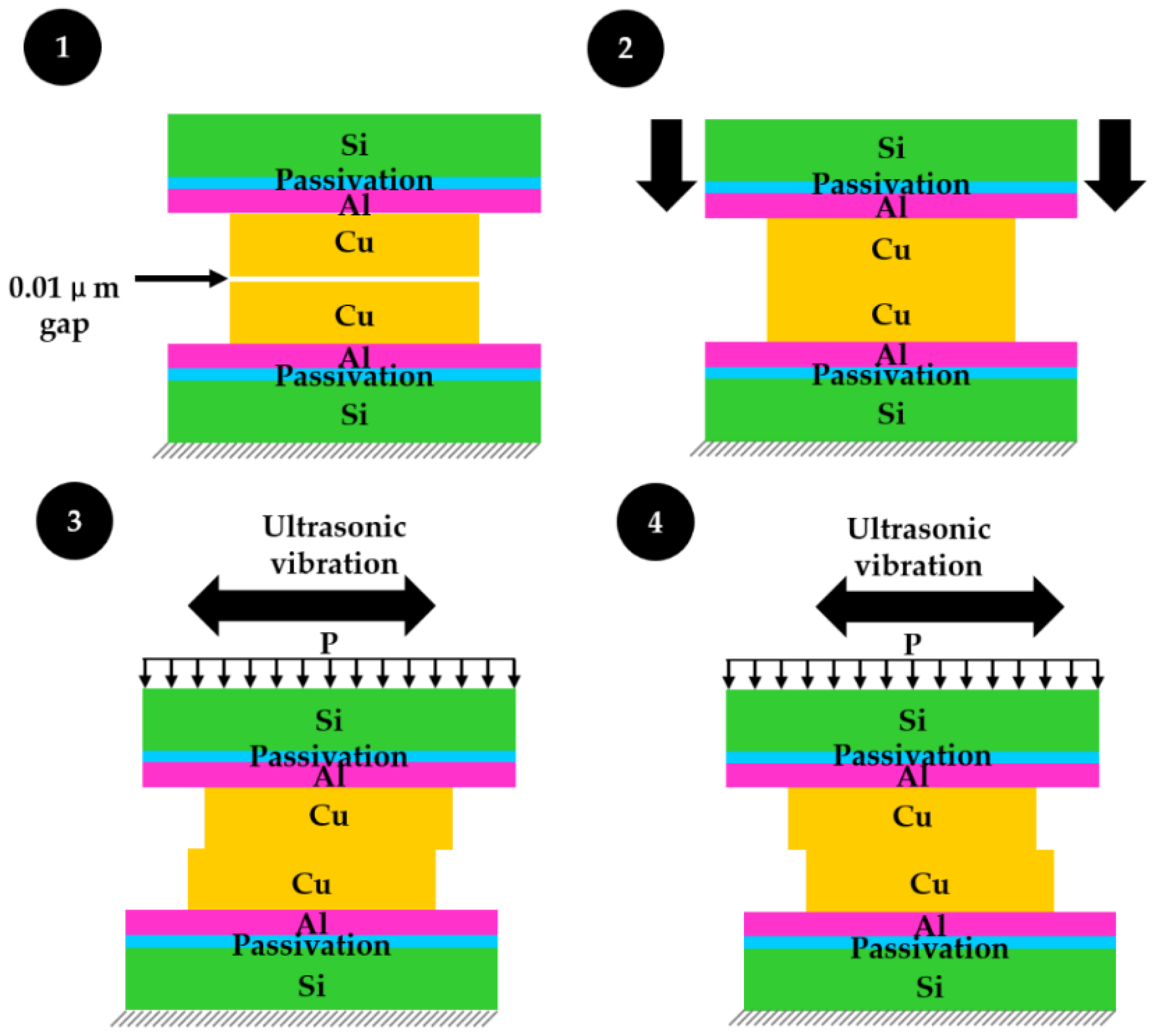
2.1. Simulation Assumptions

In general, it is difficult to simulate real situations of bonding behavior in great detail. Consequently, although we tried to explore as many relevant parameters as possible in the simulation, we had to leave out some relatively less important factors to save simulation time by establishing some basic, but reasonable, assumptions. The assumptions we made are briefly listed below:
  • The silicon wafer was assumed to be linear, elastic, and isotropic.
  • Except for the silicon wafers, the other properties of the materials had bilinear isotropic characteristics.
  • Negligible heat loss during simulated bonding.
  • With the exception of copper blocks, the material parameters at high temperatures were assumed to be the same as those at room temperature.
  • The boundary conditions at the bottom of the Si wafer layer had zero degrees of freedom in the x, y, and z directions.

2.2. Modeling and Setting of Finite Element Analysis

We selected the elements 3D solid 164 and shell 163 from ANSYS LS-DYNA for this model. It created a layer of shell 163 at the top of the model and all the surface nodes applied the load by ultrasonic vibration. In addition to the above areas, all other structures used 3D Solid 164 elements. In the selection of the material, the silicon wafer has a higher hardness and a smaller amount of relative deformation during the simulation, so it was set to linear elastic isotropic. Except for the silicon wafers, all material models were set to bilinear isotropic. A large deformation occurs in the material and plastic deformation occurs in the contact, so the elastoplastic properties must be selected for the material model in the process of ultrasonic friction. This study used thermo-solid coupling, so it was necessary to consider the effect of temperature on the material by adding some thermal parameters to the Si, while the other materials were assumed to be temperature-dependent bilinear isotropic models.

2.3. Geometry and Dimensions

This study used metric units (SI), namely length in micrometers (μm), mass in kilograms (kg), time in second (s), and temperature units in Kelvin (K). The model established in this research was the actual model size using the actual micro-copper block bonding process, as shown in Figure 1. However, Ni, IMC, and Sn2.5Ag were not included in our present study. The main research focus was on copper and copper bonding, because a copper-to-copper mono-metallic interface does not form brittle IMC phases. There is no material parameter mismatch between the same materials, such as a thermal expansion coefficient. Therefore, the focus on copper was expected to eliminate mechanical problems and to maintain stable electrical properties due to the elimination of brittle IMC formations. The upper and lower parts were in a symmetrical relationship: The lower part included, from the bottom to the top, a silicon wafer layer, protection layer, aluminum pad, and micro-copper block, and the upper part was inverted. There was a 0.01 μm interval between the two copper blocks, in order to prevent the software from judging the two copper blocks as a connection body. The origin of the model’s coordinates was at the center of the bottom silicon wafer layer, the Y axis was the direction of the vertical silicon wafer layer and the parallel silicon wafer layer was the XZ plane. The geometric dimensions of the model were adopted from Reference [20] and the geometric parameters are listed in Table 1. This study used mapped meshing to create the elements of the model. The element size sets were 1 μm and 2 μm, which divided the number of elements into groups of 10,336 and 1836, respectively. We followed Von-Mises stress and temperature at the center position of the contact surface on the bottom micro-copper bump. The maximum and deviation values are listed in Table 2 from the condition of a 50 kHz frequency. The deviation values of the maximum Von-Mises stress and maximum temperature were only 0.98% and 0.78% between element numbers 10,336 and 1836, respectively. Thus, we used element numbers 1836 as the model setting in this study. For the conversion of frictional heat generation to temperature, we use the mechanical equivalent of heat equal to 10 to speed up the analysis time. At the same temperature, the simulation time to produce the same temperature was 8.63% of the actual time. The mechanical and thermal parameters of materials at room temperature are listed in Table 3. In addition, the mechanical and thermal parameters of copper at high-temperature are listed in Table 4 and Table 5, respectively. We considered the material parameters before the copper melting point to follow the material properties of 973 K to observe the phenomenon when it was close to the melting point.

2.4. Boundary Conditions, Load, and Contact Settings

At the beginning of the simulation, the upper copper block was punched towards the lower copper block and moved downward in a parallel Y-axis direction without rotation. The next ultrasonic vibration was parallel XZ plane movement and the amplitude of vibration was 0.9 μm. In the model’s lower part, the surface was bound to the X direction and the Z direction, assuming that it extended indefinitely, except for the copper block. At the bottom of the lower silicon wafer layer, the degrees of freedom of its nodes were set to fixed. The boundary conditions of the model are plotted in Figure 2.
The process of ultrasonic friction was performed by controlling the shell 163 element of the model’s uppermost layer, because the displacement condition of the uppermost shell element drives the entire model’s upper part to move. It was an impact process during the initial time 0~2 μs of the simulation. At this stage, the upper shell element was set to move down at a constant speed of 0.005 m/s, which makes the upper copper block just touch the lower copper block. During the period of 0~2 μs, a pressure of 70 MPa was also gradually applied to the shell element. When the downward displacement distance reached 0.01 μm, it stayed at this height, and when the time reached 2 μs, the displacement constraint was removed, which was set to the constraint’s birth time and dead time. After 2~3 μs, the pressure effect on the upper copper block was moved down by 0.03 μm, starting the ultrasonic vibration for 3 μs and the correspondence between X and Z coordinates and time at different ultrasonic vibration frequencies. The TCB process of copper–copper direct bonding is shown in Figure 3.
In terms of contact setting, the top and bottom copper blocks in this study were surface-to-surface contact. This contact type is used when the face of one object penetrates the face of another object, the face-to-face contact is symmetrical, so the contact surface is equal to the target surface. The target surface and the contact surface are defined by using the nodes set. Face-to-face contact is usually used to solve the problem of large relative sliding between two objects. Then, the coefficient of friction is 0.2 [27] between the copper contact surface.

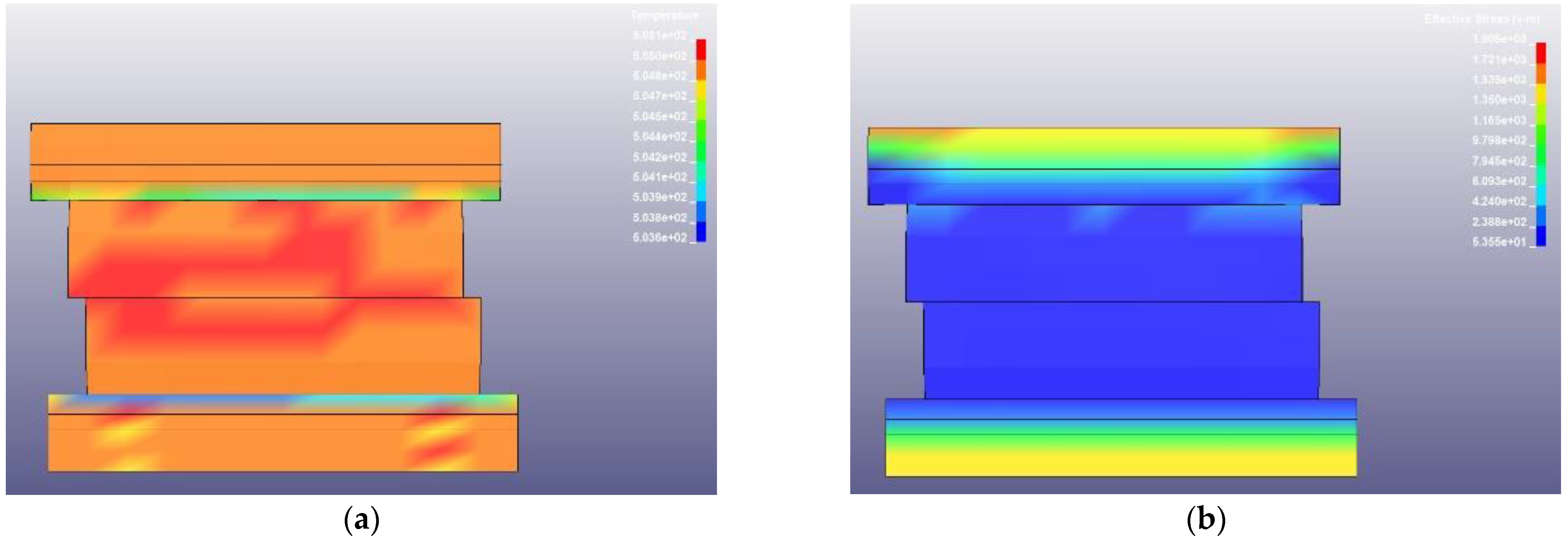
3. Results and Discussion

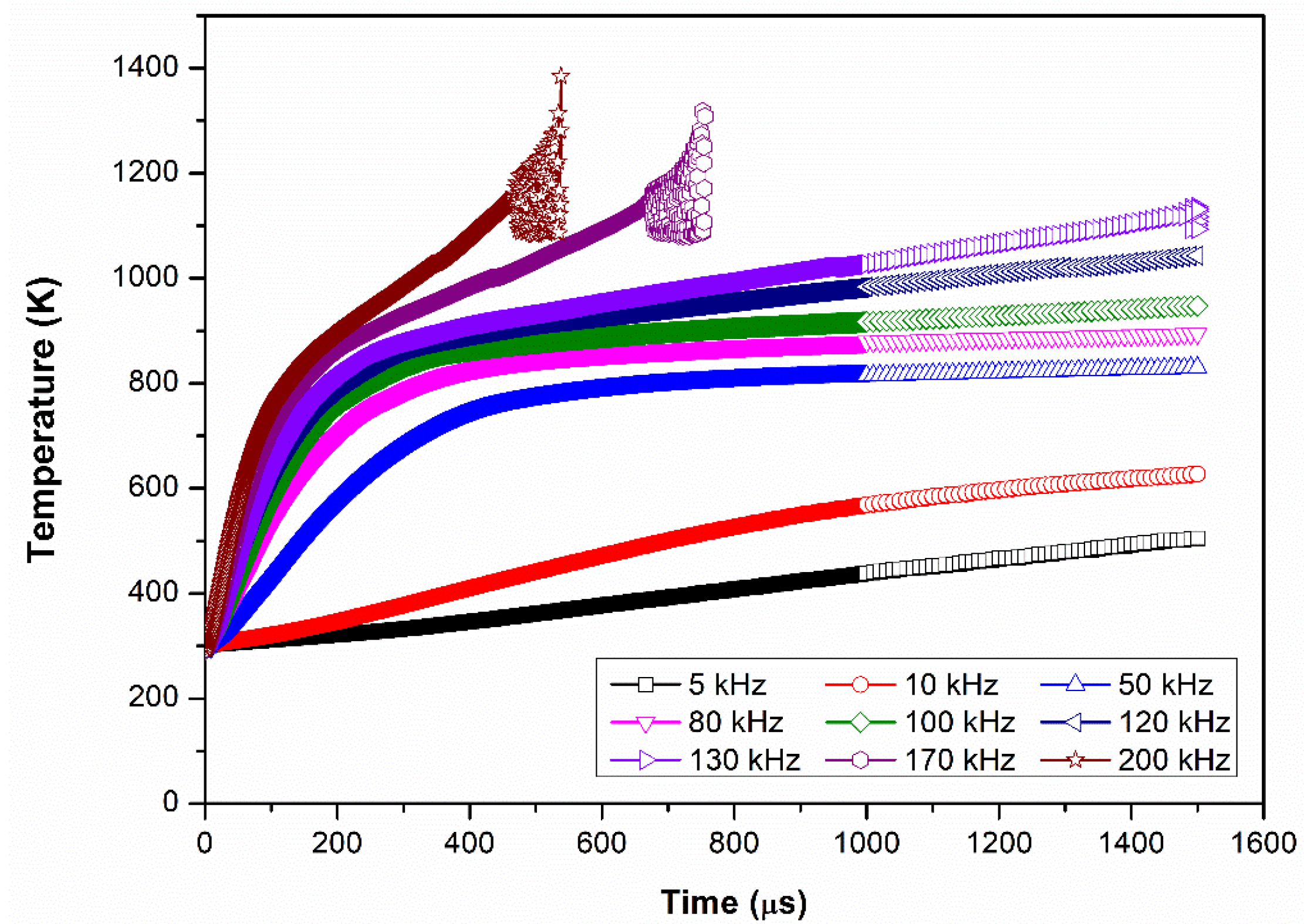
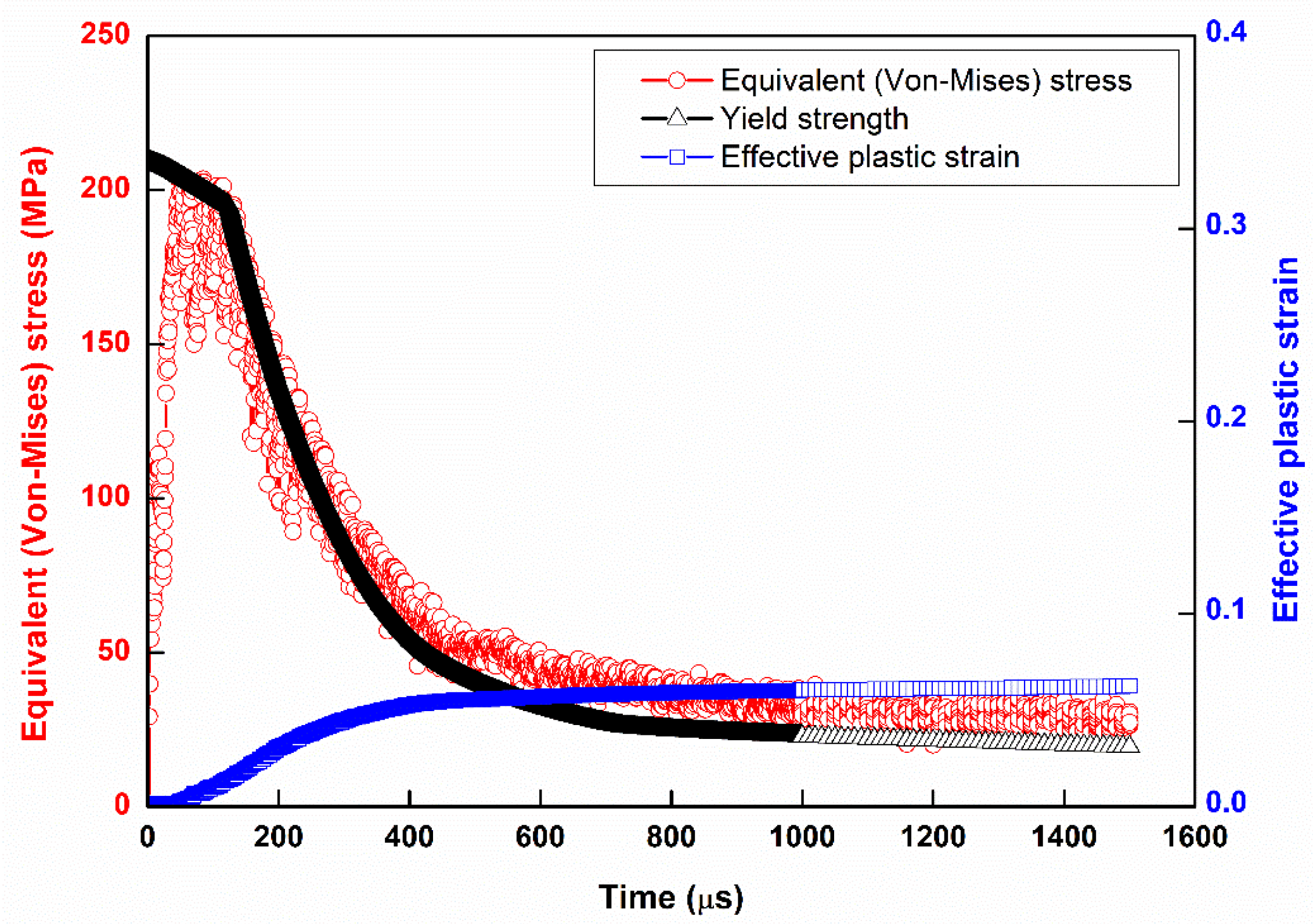
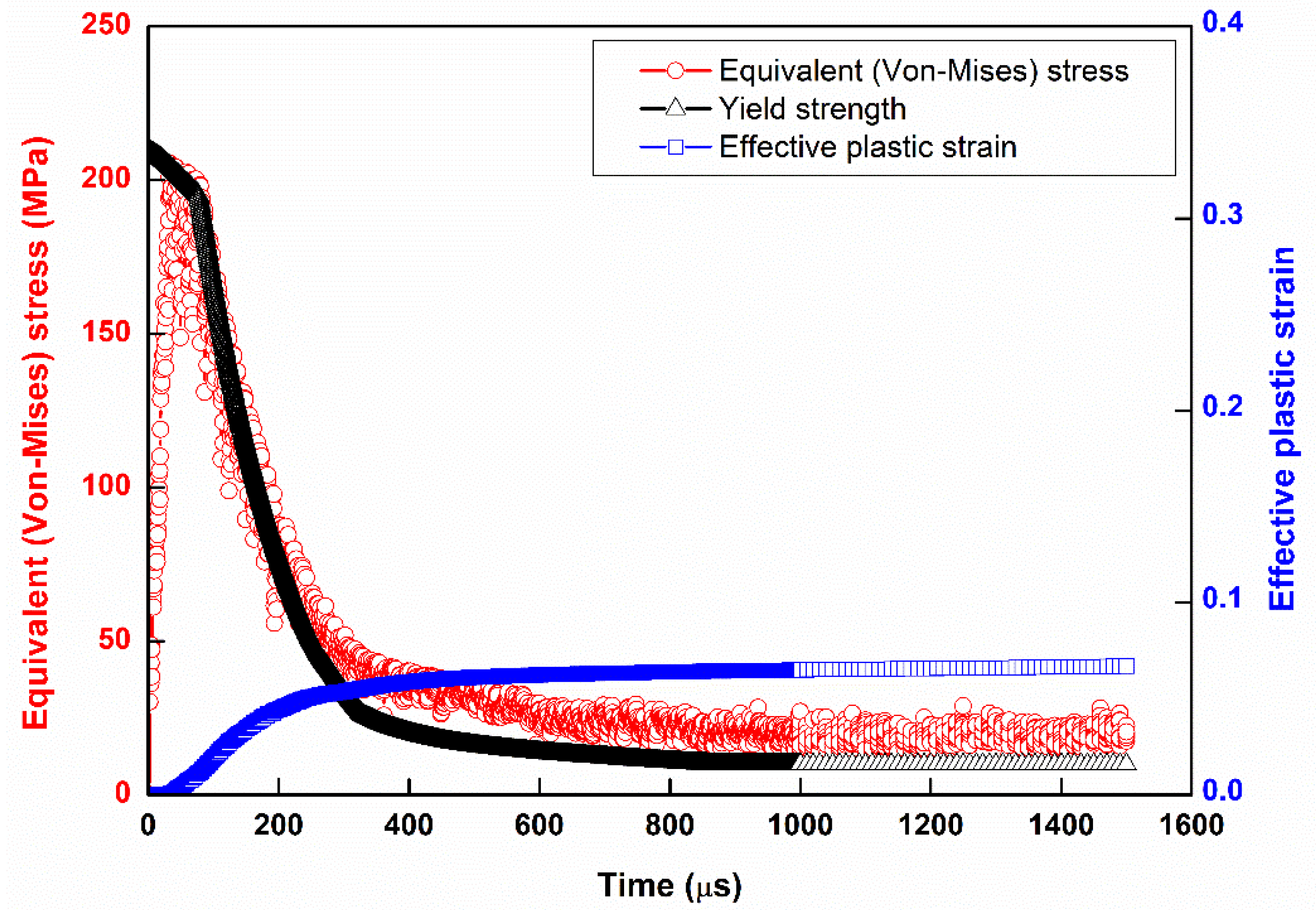
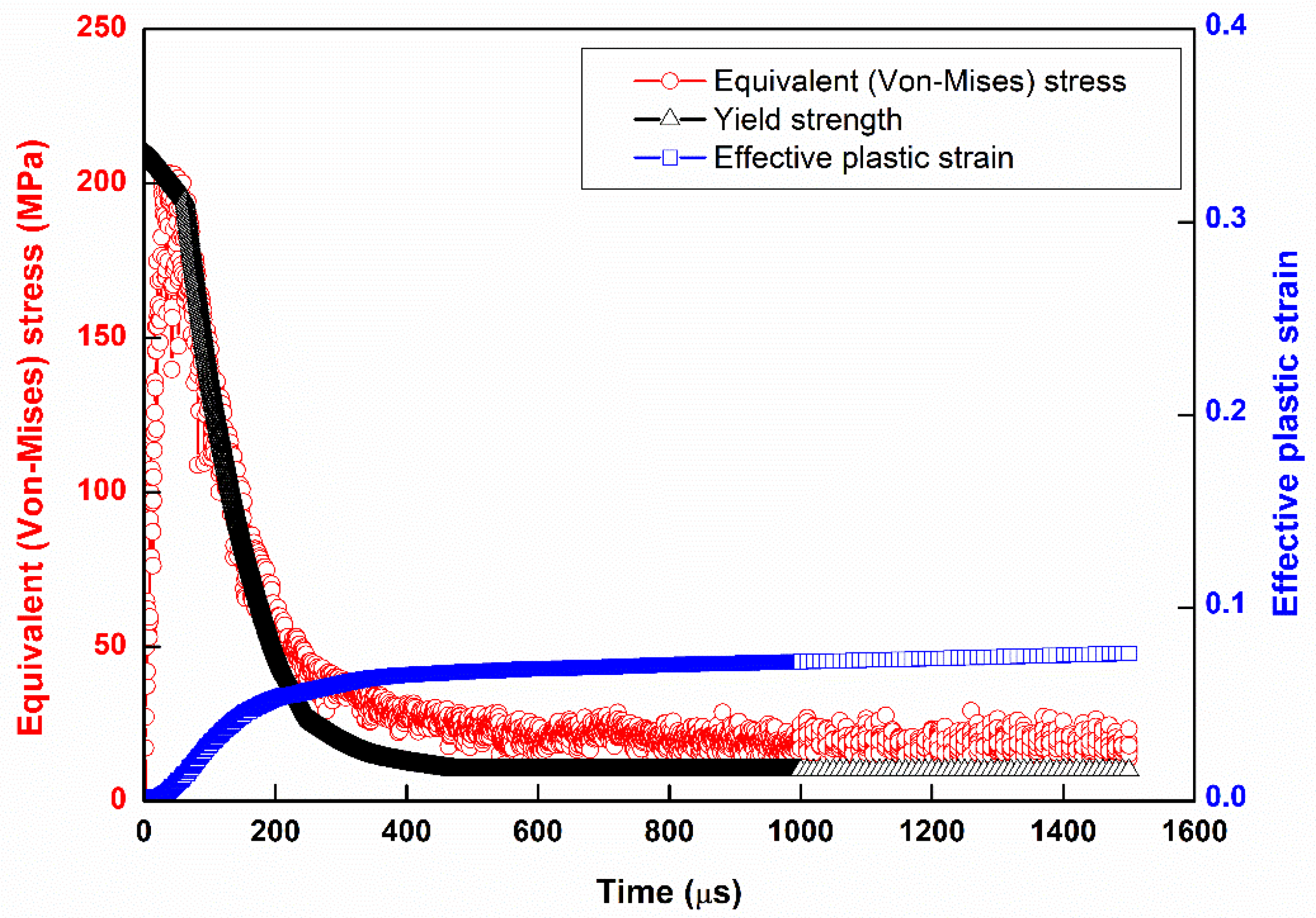
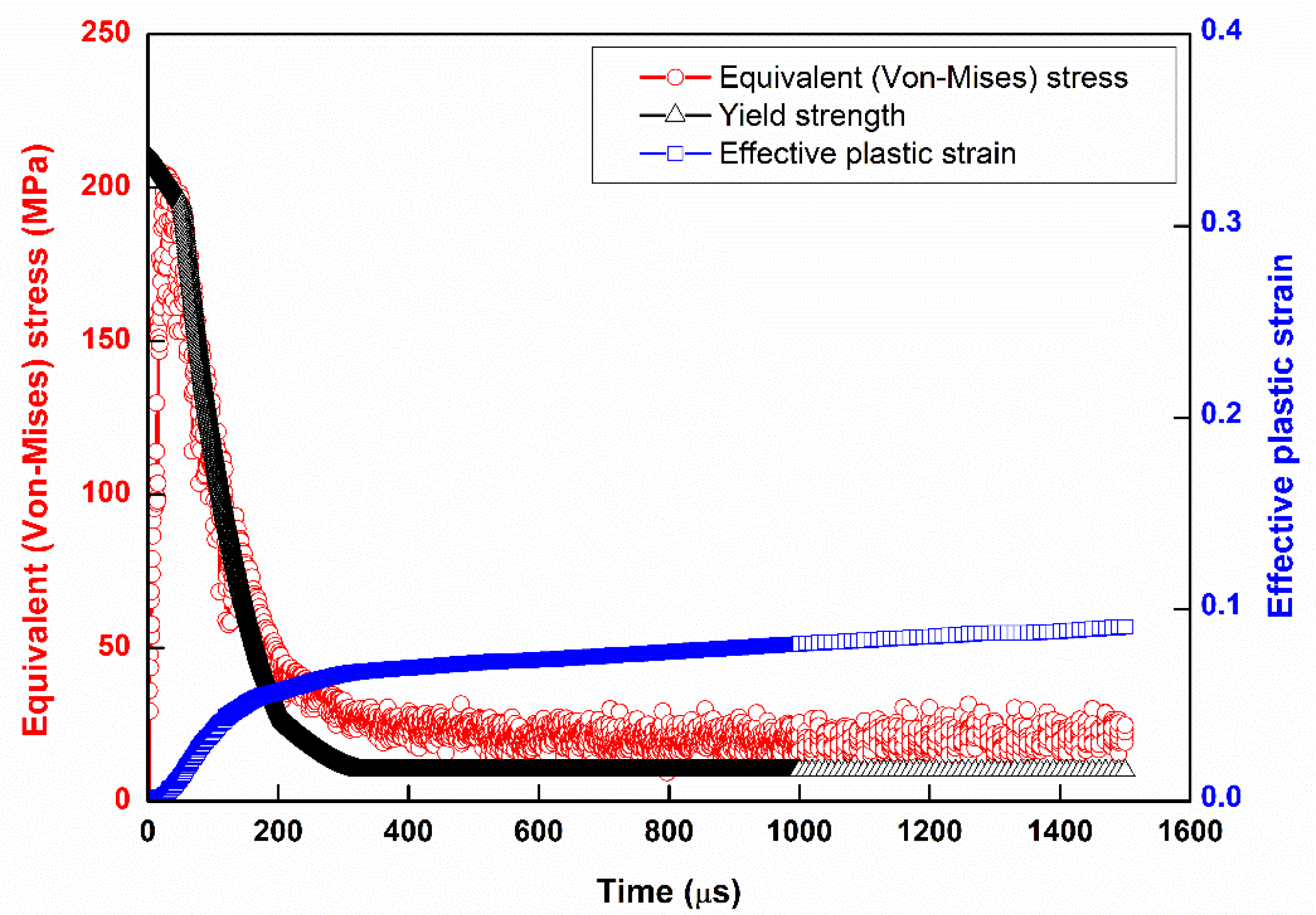
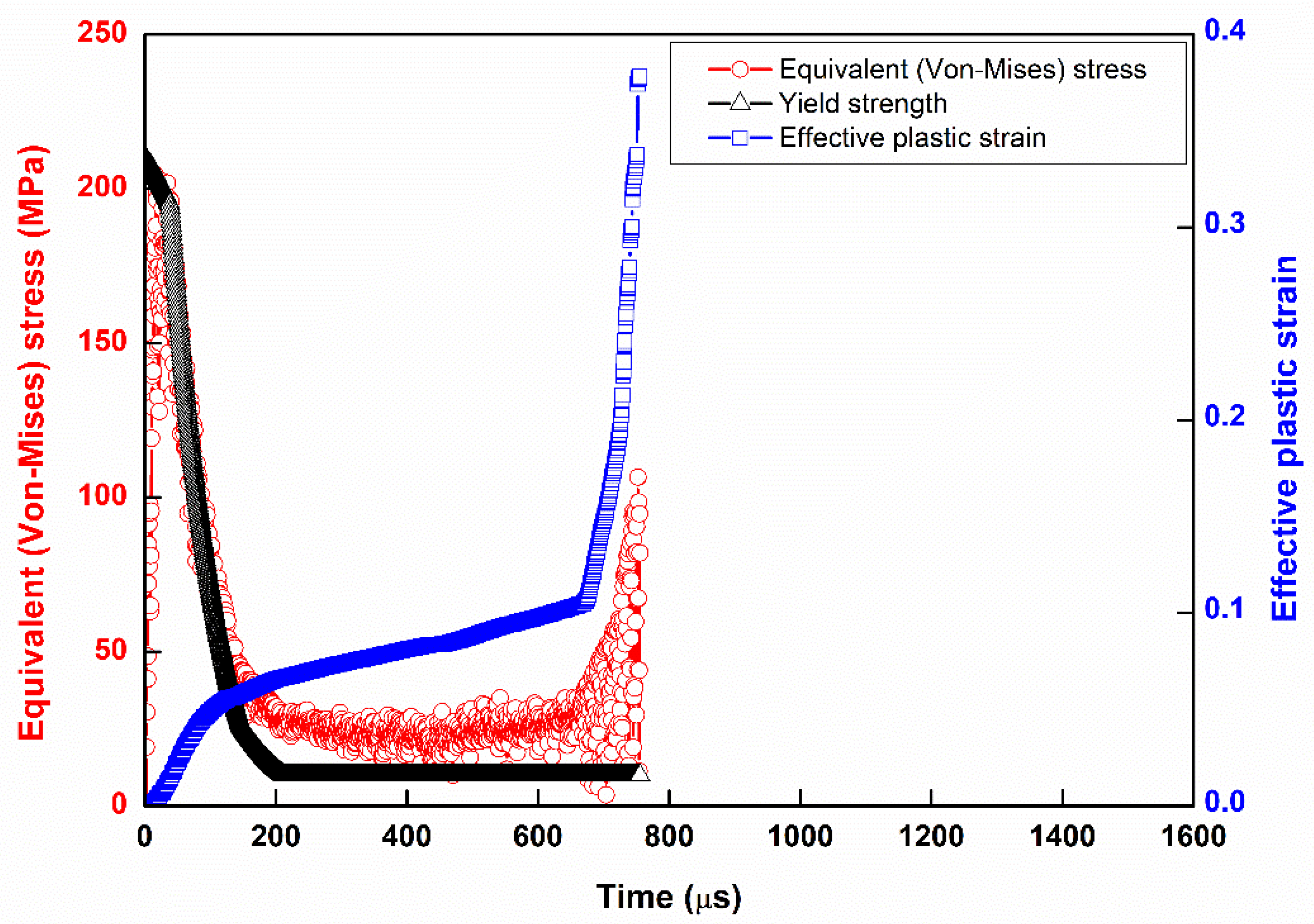
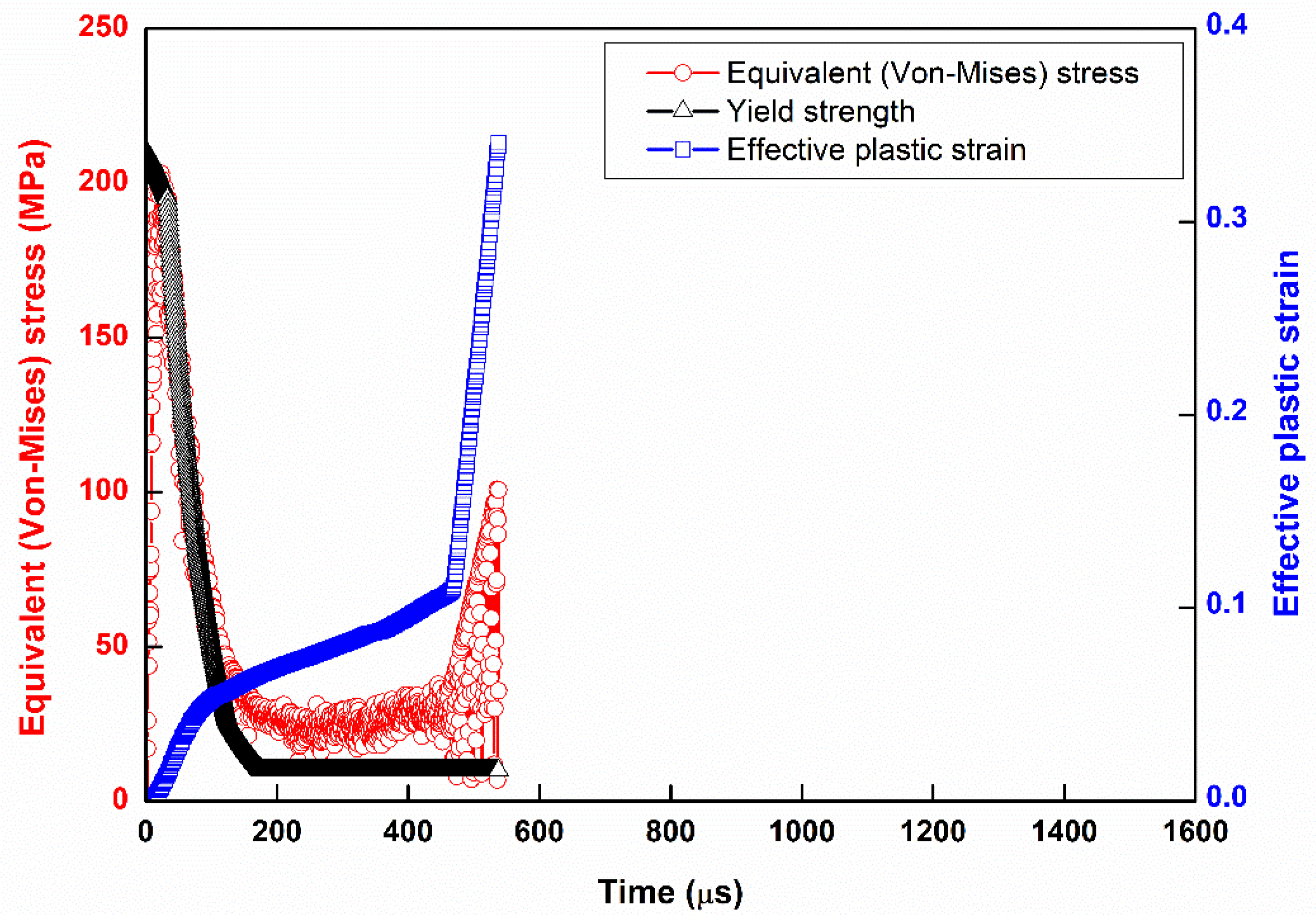
3.1. The Yield Strength Depends on the Temperature Result for Each Frequency

The temperature results of ultrasonic vibration frequency are shown in Figure 4. The simulation results produce a temperature value that changes over time for each frequency. Combining the results of the yield strength and temperature of copper, the yield strength curves of the TCB process for each frequency were obtained. The yield strength curve could be an index for Von-Mises stress in the process of reaching the material yield state, or not. There was a severe temperature shock in the end of the temperature range at frequencies of 130 kHz, 170 kHz, and 200 kHz. At the frequencies of 170 kHz and 200 kHz, not only was there severe shock, but they also stopped the simulation time early. The results are discussed in detail in later sections.

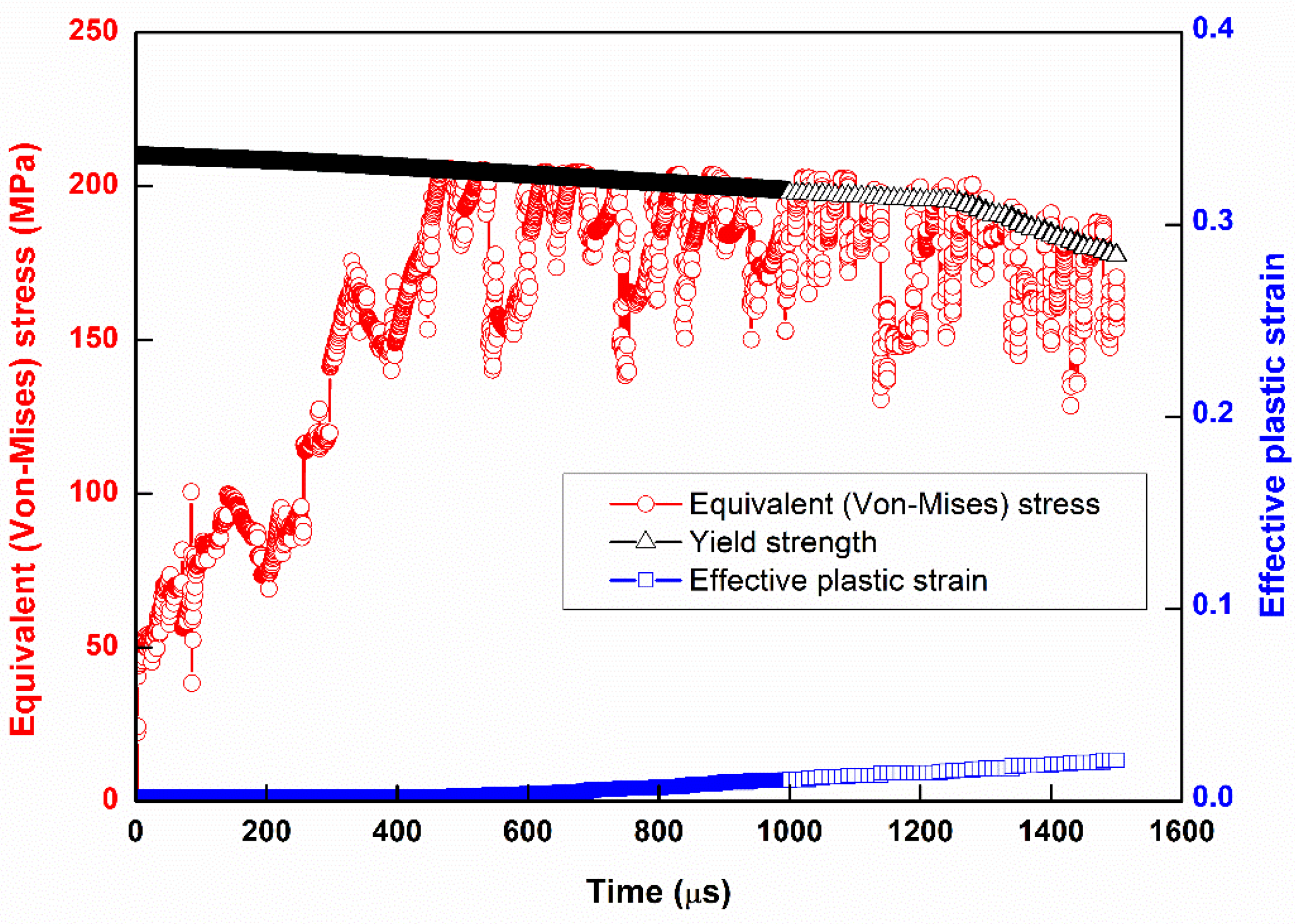
3.2. Strain Softening

According to Figure 3, the simulation process is an iterative behavior of ultrasonic vibration: even if the model results from different frequencies are shown, only the result value changes. It is not easy to observe the phenomenon from the model result graph as shown in Figure 5a, and the maximum value in the contour is affected by the stress concentration of the geometric effect, as shown in Figure 5b. The results of the study are continued over time, and the location of the discussion is at the center of the contact surface. Therefore, we used the curve to express the results, so that we could directly understand the difference between different frequencies. The curves of equivalent stress and plastic strain of the copper block at the frequency of 5 kHz are plotted in Figure 6. It was found that the yielding strength curve decreased slowly. In addition, the equivalent stress increased to 22 MPa from 0 μs to 3 μs. Then, it reaches a maximum value of 205.84 MPa in 3–470 μs. After that, the stress was decreased slightly and reached a value of about 165.27 MPa. The corresponding plastic strain and temperature were 0.02 and 505 K. Considering the frequency of 10 kHz in Figure 7, the depression of the copper block brought the stress value to 28 MPa. The equivalent stress was increased to reach a maximum value of 205.84 MPa within the time of 3–234 μs and the final value was about 125.48 MPa. In addition, the corresponding plastic strain and temperature were 0.04 and 627 K, respectively.
An equivalent stress curve at 50 kHz that clearly divides the curve into three parts is plotted in Figure 8. The first part is the stress rise stage caused by the copper block being pushed down for 0~3 μs. The ultrasonic vibration was carried out at 3 μs and the equivalent stress reached about 25 MPa. Furthermore, the equivalent stress kept increasing because of the repeating friction effects on the copper blocks. Thus, it can be observed that the equivalent stress reached a maximum value of 204 MPa at the time of 56.5 μs, indicating the “simultaneous several lattice slip region” [28]. A modeling of ultrasonic hardening and softening was carried out. The analytical model was constructed by the generalization of the synthetic theory of plastic deformation. The ultrasonic defect intensity was thus introduced, so that the phenomenon of both hardening and softening could be described by the uniform system of constitutive equations [29]. At the beginning of the ultrasonic vibration, the entire contact surface was used as the medium when the energy was transmitted. The contact surface appears to be a hard material; therefore, the amount of deformation at this stage was relatively small. The stress value decreased from 204 MPa to 63 MPa within the time of 56.5–500 μs. In this stage, the reduction of the yielding strength of material was caused by the effects of the “friction effect” and “temperature effect”; that is, the softening phenomenon [30].
As ultrasonic energy is applied to a copper bond, only the intrinsic defects are activated [31]. Therefore, the high-density dislocation of materials is generated by the repeated stress, further becoming the strain-hardening phenomenon. Therefore, this area is called the “dislocation multiplied increasing region” [31]. On the other hand, the temperature at the interface of two copper blocks is increased significantly due to the friction effect during the ultrasonic bonding process. Thus, the temperature was clearly increased within the time of 56.5–500 μs, as shown in Figure 4. This area is called the “slip by dislocation shifting region” [32]. In addition, the high-density dislocations and the formation of atomic diffusion channels are exhibited in materials because of the repeated stress-induced stress concentration [33,34,35,36]. Therefore, the copper blocks are successfully bonded together to form a connection.
In Figure 8, the equivalent stress curve is displayed above the theoretical yield strength curve, indicating that the contact surface is in a strain-hardened state. Because the strain hardening occurred at the contact surface, the plastic strain was close to a stable value (0.06) shortly after 400 μs. It can be found that the yield strength curve of 50 kHz is significantly lower than those of 5 kHz and 10 kHz. This means the yield strength of the material was decreased at the high temperature with the aid of the bonding behavior. In addition, the temperature of the contact surface was increased to 830 K at the frequency of 50 kHz. Consequently, it was possible to make the contact surface of the two copper blocks bond at the ultrasonic vibration frequency of 50 kHz.
The equivalent stress curve at 80 kHz can also be divided into three parts and is plotted in Figure 9. The copper block was pushed down to make the equivalent stress value increase to 30 MPa within the time 0~3 μs. Then, this equivalent stress reached a maximum value of 205.43 MPa at 33 μs. Next, the equivalent stress decreased rapidly within the time of 33–300 μs and reached 33 MPa at the time of 300 μs. In addition, the plastic strain increased quickly to a value of 0.06 at 300 μs. When the frequency was higher than 50 kHz, the yield strength curve was very similar. From the temperature field of 80 kHz in Figure 4, the temperature increased and reached 827 K at 300 μs, and further increased to a stable temperature of 894 K. On the other hand, the plastic strain tended to a stable value of 0.07; the corresponding stress value was about 20.44 MPa, as displayed in Figure 9.

3.3. Strain Hardening

The equivalent stress curve at 100 kHz can also be divided into three parts and is shown in Figure 10. During the time of 0–3 μs, the copper block was pushed down to make the equivalent stress value rise to 27 MPa. then, the equivalent stress dropped very rapidly within the time of 33–300 μs. In contrast, the plastic strain increased quickly during this time region. The third part is the stage of stress stabilization. Despite the oscillation behavior exhibited in the curve, the equivalent stress value tended to about 17.94 MPa. In addition, the corresponding plastic strain was 0.08. At the same time, the temperature reached to 947 K, as shown in Figure 4.
The equivalent stress curve at 120 kHz can also be divided into three parts and is plotted in Figure 11. At the beginning, the equivalent stress increased clearly within the time of 0–3 μs. Then, the curve dropped very rapidly within the time of 38–300 μs. Finally, the equivalent stress value, the corresponding plastic strain, and the temperature tended to about 24.73 MPa, 0.09, and 1043 K, respectively.

3.4. Solid Solution State

The stress curve of 130 kHz that can be divided into four parts is displayed in Figure 12. The fourth part is presented in the solid solution. The first part was the stress rising stage from time 0~3 μs. Then, the stress dropped very rapidly within the time of 33–300 μs. The plastic strain increased quickly in the initial stage and finally tended to stable after 300 μs. From the stress distribution at the curve end of 28.04 MPa, it can be found that the tendency of the vibration amplitude was no longer stable, which is the difference of the above-mentioned three stages. In addition, the plastic strain also presented a larger value.
In Figure 4, it is interesting to note that the oscillation behavior (so-called a solid solution phenomenon) is observed at the temperature of 1131 K for the frequency of 130 kHz. Moreover, the smaller stress value corresponds the larger strain value at the same time and can be found in Figure 12. Therefore, the material temperature was increased in the solid solution via the friction and temperature effects, resulting in a softer material and larger plastic strain (0.11).

3.5. Solid Solution Time Point Advances with Frequency

The stress curves of 170 kHz and 200 kHz are divided into four parts, as shown in Figure 13 and Figure 14, respectively. For 170 kHz, the equivalent stress value, the corresponding plastic strain, and the temperature tended to about 81.94 MPa, 0.37, and 1307 K, respectively. For 200 kHz, the equivalent stress value, the corresponding plastic strain, and the temperature tended to about 100.65 MPa, 0.34, and 1384 K, respectively. As the mentioned above, the equivalent stress, plastic strain, and temperature increased with increasing ultrasonic vibration frequency. The solid solution occurred earlier as the frequency increased, and the solid solution in 170 kHz appeared at 650 μs and the in 200 kHz occurred at 450 μs. All the values of stress, strain, and temperature for different frequencies are listed in Table 6.

4. Conclusions

The three-dimensional simulation model of the ultrasonic vibration bonding process of micro-copper blocks was investigated by using the finite element method. The effects of ultrasonic vibration frequency on the stress field, strain field, and temperature field at the copper bump joint surface were discussed. The main findings are summarized as follows:
  • By using other frequencies to compare with the simulation results of 50 kHz, it can be found that the bonding phenomenon will not occur in the simulation time of 1500 μs if the frequency is lower than 50 kHz.
  • The low temperature copper-to-copper bonding technology requires lower temperature (573 K) and a shorter bonding time (100 s), establishing the effectiveness of this better bonding method by improving the reduction of temperature and time with the TCB by 100 times. This research will have a major impact on the industry.
  • From the high frequency simulation, it was found that the end of the curve was in the solid solution phase. Near the end of the simulation, it can be found that the trend of the amplitude of the vibration (similarly to the temperature curve) becomes larger from the stress distribution. That is, the materials structure at this stage is not very stable. For this phenomenon, it is called a solid solution.

Author Contributions

Conceptualization, Y.-M.H., C.-T.P., B.-S.C., and S.-R.J.; methodology, Y.-M.H., C.-T.P., and B.-S.C.; formal analysis, B.-S.C.; resources, Y.-M.H., C.-T.P., and S.-R.J.; writing—original draft preparation, Y.-M.H., C.-T.P., B.-S.C., and S.-R.J.; writing—review and editing, S.-R.J.; funding acquisition, S.-R.J. All authors have read and agreed to the published version of the manuscript.

Funding

The authors are thankful for the financial support from the Ministry of Science and Technology, Taiwan under Contract Nos. MOST 109-2221-E-214-016.

Institutional Review Board Statement

Not applicable.

Informed Consent Statement

Not applicable.

Data Availability Statement

All data generated or analyzed during this study are included in this article.

Conflicts of Interest

The authors declare no conflict of interest.

References

  1. Topol, A.W.; La Tulipe, D.C.; Shi, L.; Frank, D.J.; Bernstein, K.; Steen, S.E.; Kumar, A.; Singco, G.U.; Young, A.M.; Guarini, K.W.; et al. Three-dimensional integrated circuits. IBM J. Res. Dev. 2006, 50, 491–506. [Google Scholar] [CrossRef]
  2. Patti, R.S. Three-dimensional integrated circuits and the future of system-on-chip designs. Proc. IEEE Inst. Electr. Electron. Eng. 2006, 94, 1214–1224. [Google Scholar] [CrossRef]
  3. Ruythooren, W.; Beltran, A.; Labie, R. Cu-Cu bonding alternative to solder based micro-bumping. In Proceedings of the 2007 9th Electronics Packaging Technology Conference, Singapore, 10 December 2007; pp. 315–318. [Google Scholar]
  4. Tu, K.N. Reliability challenges in 3D IC packaging technology. Microelectron. Reliab. 2011, 51, 517–523. [Google Scholar] [CrossRef]
  5. Motoyoshi, M. Through-silicon via (TSV). Proc. IEEE Inst. Electr. Electron. Eng. 2009, 97, 43–48. [Google Scholar] [CrossRef]
  6. Hu, Y.H.; Liu, C.S.; Lii, M.J.; Manna, A.L.; Rebibis, K.J.; Zhao, M.; Beyne, E.; Yu, C.H. 3D stacking using Cu-Cu direct bonding for 40um pitch and beyond. In Proceedings of the 2012 4th Electronic System-Integration Technology Conference (ESTC 2012), Amsterdam, The Netherlands, 17–20 September 2012; pp. 1–5. [Google Scholar]
  7. Daily, R.; Teng, W.; Capuz, G.; Miller, A. Microscrubbing: An alternative method for 3D thermocompression bonding CuCu bumps and high bump density devices with low force, time and temperature. In Proceedings of the 2013 IEEE 63rd Electronic Components and Technology Conference, Las Vegas, NV, USA, 28–31 May 2013; pp. 255–259. [Google Scholar]
  8. Chen, K.N.; Fan, A.; Tan, C.S.; Reif, R. Temperature and duration effect on microstructure evolution during copper wafer bonding. J. Electron. Mater. 2003, 32, 1371–1374. [Google Scholar] [CrossRef] [Green Version]
  9. Lin, S.K.; Wang, M.J.; Yeh, C.Y.; Chang, H.M.; Liu, Y.C. High-strength and thermal stable Cu-to-Cu joint fabricated with transient molten Ga and Ni under-bump-metallurgy. J. Alloys Compd. 2017, 702, 561–567. [Google Scholar] [CrossRef]
  10. Wu, B.; Zhang, S.; Wang, F.; Chen, Z. Micro copper pillar interconnection using thermosonic flip chip bonding. J. Electron. Packag. 2018, 140, 044502. [Google Scholar] [CrossRef]
  11. Li, J.; Zhang, Y.; Zhang, H.; Chen, Z.; Zhou, C.; Liu, X.; Zhu, W. The thermal cycling reliability of copper pillar solder bump in flip chip via thermal compression bonding. Microelectron. Reliab. 2020, 104, 113543. [Google Scholar] [CrossRef]
  12. Srinivasan, V.P.; Balamurugan, S.; Balakarthick, B.; Devva Darshan, S.; Dhanush Prabhu, A.B. Experimental investigation on ultrasonic metal welding of copper sheet with copper wire using Taguchi method. Mater. Today Proc. 2020, in press. [Google Scholar] [CrossRef]
  13. Watanabe, N.; Asano, T. Room-temperature Cu-Cu bonding in ambient air achieved by using cone bump. Appl. Phys. Express 2010, 4, 016501. [Google Scholar] [CrossRef]
  14. Iwanabe, K.; Shuto, T.; Noda, K.; Nakai, S.; Asano, T. Room-temperature microjoining using ultrasonic bonding of compliant bump. In Proceedings of the 2012 3rd IEEE International Workshop on Low Temperature Bonding for 3D Integration, Tokyo, Japan, 22–23 May 2012; pp. 167–170. [Google Scholar]
  15. Chang, J.Y.; Cheng, R.S.; Kao, K.S.; Chang, T.C.; Chuang, T.H. Reliable microjoints formed by solid-liquid interdiffusion (SLID) bonding within a chip-stacking architecture. IEEE Trans. Compon. Packag. Manuf. Technol. 2012, 2, 979–984. [Google Scholar] [CrossRef]
  16. Klumpp, A.; Merkel, R.; Ramm, P.; Weber, J.; Wieland, R. Vertical system integration by using inter-chip vias and solid-liquid interdiffusion bonding. Jpn. J. Appl. Phys. 2004, 43, L829. [Google Scholar] [CrossRef]
  17. Pan, C.T.; Yang, H.; Shen, S.C.; Chou, M.C.; Chou, H.P. A low-temperature wafer bonding technique using patternable materials. J. Micromech. Microeng. 2002, 12, 611. [Google Scholar] [CrossRef]
  18. Nguyen, T.H.; Thanh, L.Q.; Loc, N.H.; Huu, M.N.; Nguyen Van, A. Effects of Different Roller Profiles on the Microstructure and Peel Strength of the Ultrasonic Welding Joints of Nonwoven Fabrics. Appl. Sci. 2020, 10, 4101. [Google Scholar] [CrossRef]
  19. Ng, R.; Nai, M.L.S.; Chan, H.L.I.; Shi, C.W.P.; Song, B. Comparative eco-efficiency analyses of copper to copper bonding technologies. Procedia CIRP 2014, 15, 96–104. [Google Scholar] [CrossRef] [Green Version]
  20. Lee, C.C.; Yang, T.F.; Wu, C.S.; Kao, K.S.; Cheng, R.C.; Chen, T.H. Reliability estimation and failure mode prediction for 3D chip stacking package with the application of wafer-level underfill. Microelectron. Eng. 2013, 107, 107–113. [Google Scholar] [CrossRef]
  21. Gao, J.; Kelly, R.; Yang, Z.; Chen, X. An investigation of capillary vibration during wire bonding process. In Proceedings of the 2008 International Conference on Electronic Packaging Technology & High Density Packaging, Shanghai, China, 28–31 July 2008; pp. 1–6. [Google Scholar]
  22. Sahani, P.; Mula, S.; Roy, P.K.; Kang, P.C.; Koch, C.C. Structural investigation of vacuum sintered Cu-Cr and Cu-Cr-4% SiC nanocomposites prepared by mechanical alloying. Mater. Sci. Eng. A 2011, 528, 7781–7789. [Google Scholar] [CrossRef]
  23. White, G.K.; Collocott, S.J. Heat Capacity of Reference Materials: Cu and W. J. Phys. Chern. Ref. Data 1984, 13. [Google Scholar] [CrossRef]
  24. Incropera, F.P.; Dewitt, D.P. Fundamentals of Heat and Mass Transfer, 2nd ed.; John Wiley & Sons: Hoboken, NJ, USA, 1985. [Google Scholar]
  25. Miller, T.J.; Zinkle, S.J.; Chin, B.A. Strength and Fatigue of Dispersion-Strengthened Copper. J. Nucl. Mater. 1991, 178–181, 263–266. [Google Scholar] [CrossRef]
  26. Lide, D.R. (Ed.) Handbook of Chemistry and Physics, 1st ed.; CRC Press: Boca Raton, FL, USA, 2005; pp. 12–108. [Google Scholar]
  27. Liu, T. Sliding friction of copper. Wear 1964, 7, 163–174. [Google Scholar] [CrossRef]
  28. Li, J.; Fuliang, W.; Han, L.; Zhong, J. Theoretical and experimental analyses of atom diffusion characteristics on wire bonding interfaces. J. Phys. D Appl. Phys. 2008, 41, 135303. [Google Scholar] [CrossRef]
  29. Rusinko, A. Analytical description of ultrasonic hardening and softening. Ultrasonics 2011, 51, 709–714. [Google Scholar] [CrossRef] [PubMed]
  30. Murali, S.; Srikanth, N.; Vath III, C.J. Grains, deformation substructures, and slip bands observed in thermosonic copper ball bonding. Mater. Charact. 2003, 50, 39–50. [Google Scholar] [CrossRef]
  31. Srikanth, N.; Murali, S.; Wong, Y.M.; Vath, C.J., III. Critical study of thermosonic copper ball bonding. Thin Solid Films 2004, 462–463, 339–345. [Google Scholar] [CrossRef]
  32. Levine, L. The ultrasonic wedge bonding mechanism: Two theories converge. Proc. SPIE 1995, 2649, 242. [Google Scholar]
  33. Wang, F.; Han, L.; Zhong, J. Stress-induced atom diffusion at thermosonic flip chip bonding interface. Sens. Actuator A Phys. 2009, 149, 100–105. [Google Scholar] [CrossRef]
  34. Wang, F.; Han, L. Ultrasonic effects in the thermosonic flip chip bonding process. IEEE Trans. Compon. Packag. Manuf. Technol. 2013, 3, 336–341. [Google Scholar] [CrossRef]
  35. Li, J.H.; Han, L.; Duan, J.A.; Zhong, J. Microstructural characteristics of Au/Al bonded interfaces. Mater. Charact. 2007, 58, 103–107. [Google Scholar] [CrossRef]
  36. Siddiq, A.; Ghassemieh, E. Thermomechanical analyses of ultrasonic welding process using thermal and acoustic softening effects. Mech. Mater. 2008, 40, 982–1000. [Google Scholar] [CrossRef]
Figure 1. Appearance of a simulation model: (a) XY-axis plane (b) Upper and bottom copper blocks (c) XYZ-axis direction (d) Three-dimensional mesh for micro-copper bumps.
Metals 11 00460 g001
Figure 2. The boundary conditions of the model.
Metals 11 00460 g002
Figure 3. Schematic representation of the copper–copper direct bonding for the thermal compression bonding (TCB) process: (1) Geometric static state. (2) The upper bump is pressed down. (3) Ultrasonic vibration on the upper bump. (4) The upper bump moves repeatedly under the influence of ultrasonic vibration.
Metals 11 00460 g003
Figure 4. The temperature curves of the ultrasonic vibration frequencies.
Metals 11 00460 g004
Figure 5. The results distribution of the simulation model at the frequency of 5 kHz: (a) The temperature distribution maximum value is 5.051∙102 K and (b) the stress distribution maximum value is 1.906∙103 MPa at the end of the simulation time.
Metals 11 00460 g005
Figure 6. The equivalent (Von-Mises) stress, yield strength, and effective plastic strain for a 5 kHz frequency.
Metals 11 00460 g006
Figure 7. The equivalent (Von-Mises) stress, yield strength, and effective plastic strain for a 10 kHz frequency.
Metals 11 00460 g007
Figure 8. The equivalent (Von-Mises) stress, yield strength, and effective plastic strain for a 50 kHz frequency.
Metals 11 00460 g008
Figure 9. The equivalent (Von-Mises) stress, yield strength, and effective plastic strain for a 80 kHz frequency.
Metals 11 00460 g009
Figure 10. The equivalent (Von-Mises) stress, yield strength, and effective plastic strain for a 100 kHz frequency.
Metals 11 00460 g010
Figure 11. The equivalent (Von-Mises) stress, yield strength, and effective plastic strain for a 120 kHz frequency.
Metals 11 00460 g011
Figure 12. The equivalent (Von-Mises) stress, yield strength, and effective plastic strain for a 130 kHz frequency.
Metals 11 00460 g012
Figure 13. The equivalent (Von-Mises) stress, yield strength, and effective plastic strain for a 170 kHz frequency.
Metals 11 00460 g013
Figure 14. The equivalent (Von-Mises) stress, yield strength, and effective plastic strain for a 200 kHz frequency.
Metals 11 00460 g014
Table 1. Geometric parameters [20].
MaterialLength (μm)Width (μm)Height (μm)
Copper (Small)12121.0
Copper (Big)20205.0
Aluminum Pad24241.0
Passivation24240.8
Silicon24242.1
Table 2. The mesh convergence analysis for Von-Mises stress and temperature.
Total ElementsMax. Von-Mises Stress (MPa)Max. Temperature (K)
10,336202.0823.5
1836204.0830.0
Deviation value (%)0.98%0.78%
Table 3. The material parameters at room temperature (293 K) [21].
PropertyCopperAluminumPassivationSilicon
Density (kg/m3)8910271013102330
Young’s Modulus (GPa)1306932180
Poisson’s Ratio0.380.330.240.30
Yielding Strength (GPa)0.210.400.35-
Tangent Modulus (GPa)0.601.383.20-
Specific Heat (J/Kg·K)383900940702
Thermal Conductivity (W/m·K)4003000.2148
Coefficient of thermal expansion, CTE (ppm/K)15.423.43.228.0
Table 4. The mechanical parameters of copper at different temperatures [22,23,24,25,26].
Temperature (K)Young’s Modulus (GPa)Yielding Strength (GPa)Tangent Modulus (GPa)CTE (ppm/K)
293130.00.2100.60015.40
47394.50.1950.43616.60
57388.00.1400.40817.49
80073.20.0260.33919.32
87368.40.0100.39120.00
97368.40.0100.27120.00
1358 168.40.0100.27120.00
1 Copper melting temperature.
Table 5. The thermal parameters of copper at different temperatures [22,23,24,25,26].
Temperature (K)Specific Heat (J/Kg·K)Thermal Conductivity (W/m·K)
293383400
373394395
473405388
573414381
800422374
873429367
973447354
1358 1447354
1 Copper melting temperature.
Table 6. Von-mises Stress, effective strain, and temperature at each frequency.
Frequency (kHz)Von Mises Stress (MPa)Effective StrainTemperature (K)
5165.270.02505
10125.480.04627
5027.310.06830
8020.440.07894
10017.940.08947
12024.730.091043
13028.040.111131
17081.940.371307
200100.650.341384
Publisher’s Note: MDPI stays neutral with regard to jurisdictional claims in published maps and institutional affiliations.

