Article

Deposition of Superconducting Nb3Sn Coatings Using Multiple Magnetron Sputtering Techniques

1
B.P. Veinberg Research and Educational Centre, Tomsk Polytechnic University, 30 Lenina av., 634050 Tomsk, Russia
2
E. Zuev Institute of Atmospheric Optics of Siberian Branch of the Russian Academy of Science, 1 Academician Zuev Square, 634055 Tomsk, Russia
*
Author to whom correspondence should be addressed.
Metals 2023, 13(10), 1730; https://doi.org/10.3390/met13101730
Submission received: 12 September 2023 / Revised: 9 October 2023 / Accepted: 10 October 2023 / Published: 12 October 2023
(This article belongs to the Section Metallic Functional Materials)

Abstract

:
This paper describes the elemental and phase composition, microstructure, and superconducting properties of Nb3Sn deposited by magnetron sputtering. The films were deposited on sapphire substrates using three different techniques: co-evaporation, layer-by-layer deposition of Nb and Sn, and sputtering of a stoichiometric Nb3Sn target. The influence of magnetron operation mode on the as-deposited film element composition is described. After high-temperature annealing at 700–900 °C, the results indicate the formation of superconductive films. The highest critical temperature of 16.9 K was obtained for the film deposited at a stoichiometric Nb3Sn target and annealed at a temperature of 800 °C for 12 h. These results could be used for superconducting radio-frequency applications.

1. Introduction

Superconducting radio-frequency (SRF) cavities are used in many modern accelerators and can achieve exceptionally high Q-factor values, more than six orders of magnitude higher than traditional conducting resonators [1,2,3,4,5]. To date, the main material used for SRF cavities is Nb, which has a sufficiently high critical temperature and a magnitude of the critical magnetic field.
However, despite the existence of well-tested and proven technologies for producing Nb cavities, a significant disadvantage of pure Nb is its high cost and complexity of processing [6,7,8]. An alternative approach involves the use of thin-film coatings made of niobium, while the resonator itself can be made, for instance, of copper, and a coating thickness sufficient to preserve its superconducting properties when exposed to an RF field does not need to exceed units of microns [9,10]. Thus, the limits of “traditional” SRF cavities based on niobium coatings are practically achieved.
In this regard, the use of Nb3Sn coatings, which have almost double the magnetic superheating field of 400 mT and a higher superconducting critical temperature of 18.3 K, seems very promising [11,12,13,14,15,16]. To date, several different methods have been proposed and developed for Nb3Sn thin film deposition. One approach is to immerse niobium resonators in molten tin followed by sintering; however, as a result of this process, tin droplets and undesirable tin-rich phases may remain on the surface [17].
A variant of co-evaporation of materials using electron beams was also used, accompanied by the deposition of coatings from the vapor fraction; however, the coatings formed were characterized by structural heterogeneity [18]. Attempts were made to use a method of chemical deposition from the gas phase, but the obtained resonators did not demonstrate high gradients of the accelerating field [19].
The method that is in practical use today, originally developed at Siemens, consists of saturating niobium resonators with tin vapors in high-vacuum furnaces at a temperature of about 1100–1200 °C, and it is possible to obtain coatings with a thickness of up to several microns [9]. At the moment, active work is underway to improve this method, and unique results have been obtained (for example, a gradient of the accelerating field up to 24 MV/m for a non-niobium resonator). The only drawback of this approach is that due to the high processing temperature (1200 °C), it is impossible to use copper as the resonator material.
Considering the significant successes in the use of the magnetron sputtering method for the formation of niobium-based coatings, in the last few years, work has significantly intensified on the possibility of using magnetrons for the formation of Nb3Sn coatings [20,21,22,23,24,25]. Experiments on layer-by-layer deposition of niobium and tin on a silicon oxide substrate were carried out in the Bell laboratory [26]. To produce Nb3Sn films, the authors used the deposition of multilayers of Nb and Sn with subsequent high-temperature treatment to form Nb3Sn. They observed the formation of Nb3Sn along with Nb6Sn5 at a temperature above 600 °C. Meanwhile, at a temperature above 800 °C, the undesired phase of Nb6Sn5 disappeared. The highest critical temperature of 17.45 K was observed for the film annealed at 850 °C.
The microstructural and superconducting properties of Nb3Sn films fabricated by co-sputtering on Nb and sapphire substrates have also been studied recently [13]. The authors observed the changes in the crystallinity and superconducting properties of these films with respect to the substrate temperature during the deposition. The highest critical temperature of 15.00 K was observed for the film deposited at 500 °C. The film deposited at room temperature with subsequent annealing at 665 °C for 3 h had a critical temperature of 15.88 K, and 17.61 K for a sample annealed at 950 °C for 3 h. They also observed the changes in the film morphology and microstructure. The process of forming this type of coating on copper and niobium substrates has also been studied [27,28,29,30].
The current work is devoted to the study of magnetron sputtered coatings based on Nb3Sn by using both a stoichiometric target and separate magnetron sources with Nb and Sn-based cathodes. Studies were conducted of the elemental and structural-phase compositions and superconducting properties of these films after annealing in a high-vacuum furnace at a temperature in the range from 700 to 900 °C.

2. Materials and Methods

The experiments were carried out using the in-house experimental setup shown in Figure 1. The setup is equipped with an efficient oil-free vacuum pumping system consisting of an AnestIwata Scroll Meister pre-vacuum pump, Shimadzu TMP-403LM turbomolecular pump, and CTI-Cryogenics ON-Board CryoPump cryogenic pump, which produces a high residual vacuum up to 1 × 10⁻⁵ Pa. Conducting the research under conditions of a high residual vacuum is critically important to obtain high-quality superconducting coatings with high functional properties (high critical temperature, high residual conductivity RRR, etc.).
Magnetron targets were made of Sn (purity > 99.95%, Girmet, Moscow, Russia), Nb, and stoichiometric Nb3Sn (AbleTargetLimited, Beijing, China) with a declared residual conductivity not worse than 250 RRR. To increase the cooling efficiency, a copper substrate was welded to the base of the target.
Prior to the sputtering, the experimental chamber was pumped out to a residual vacuum of at least 10−5 Pa using a cryogenic pump. Sapphires (25 × 25 × 0.5 mm3) were chosen (Techsapfir, Severniy, Russia) as a substrate material to avoid the formation of undesirable Cu–Sn phases during high-temperature annealing. Before coating deposition, the sapphire substrates were cleaned using alcohol and isopropanol and sputtered using an Ar ion source.
To form the target phase of Nb3Sn, the samples were subjected to vacuum annealing. Annealing was performed in an automated Gas Reaction Controller complex consisting of a steel vacuum chamber, a high-temperature furnace, and a controller. The controller has an electronic control system for the complex and a vacuum part. To create and maintain a vacuum in the system, a vacuum station was used, consisting of a pre-vacuum membrane and turbomolecular pumps. The prepared coatings were annealed in a steel container in a vacuum furnace under linear heating at a rate of 3 degrees per minute to the target temperature, followed by exposure for 12 h and further natural cooling down to room temperature. During the annealing process, the actual pressure in the chamber varied in the range 10−4–1.5 × 10⁻³ Pa. A typical annealing scheme (furnace pressure and temperature) is shown in Figure 2.
To control the structural and phase changes, the coatings were examined by X-ray diffraction before and after annealing. For this purpose, a Shimadzu-XRD 7000S diffractometer with a 1280-channel high-speed detector (Shimadzu, Kyoto, Japan) was used. X-ray diffraction analysis was performed by the Bragg-Brentano geometry method using Cu-Ka radiation (wavelength 1.5410 Å) at 40 kV and 30 mA. The diffraction data were analyzed using the Sleve+ program.
The microstructure and distribution of elements were analyzed using a Hitachi S-3400N (Hitachi, Tokyo, Japan) scanning electron microscope equipped with an energy-dispersive X-ray spectroscopy (EDX) attachment (Oxford Instruments, Abingdon, UK).
The morphology of the surface and the structure of the coatings were studied using a scanning electron microscope (SEM) of the Zeiss Supra 55 series (In-Lens detector type, electron energy–10 keV) with a Raith150 two electron beam exposure unit.
The superconducting properties of the films deposited on the sapphire substrates were characterized by the resistance versus the temperature data obtained from the four-point probe measurement. The samples were positioned in a copper box with electrical connectors for the readout systems. The box itself was insulated and placed in a liquid helium Dewar. A Lakeshore controller was used to measure the temperature of the sensors. The resistance values were calculated from the measured voltage of about 0.01 mV and the measured current of about 0.1 mA. DC electrical measurements were performed with Keithley 6221.

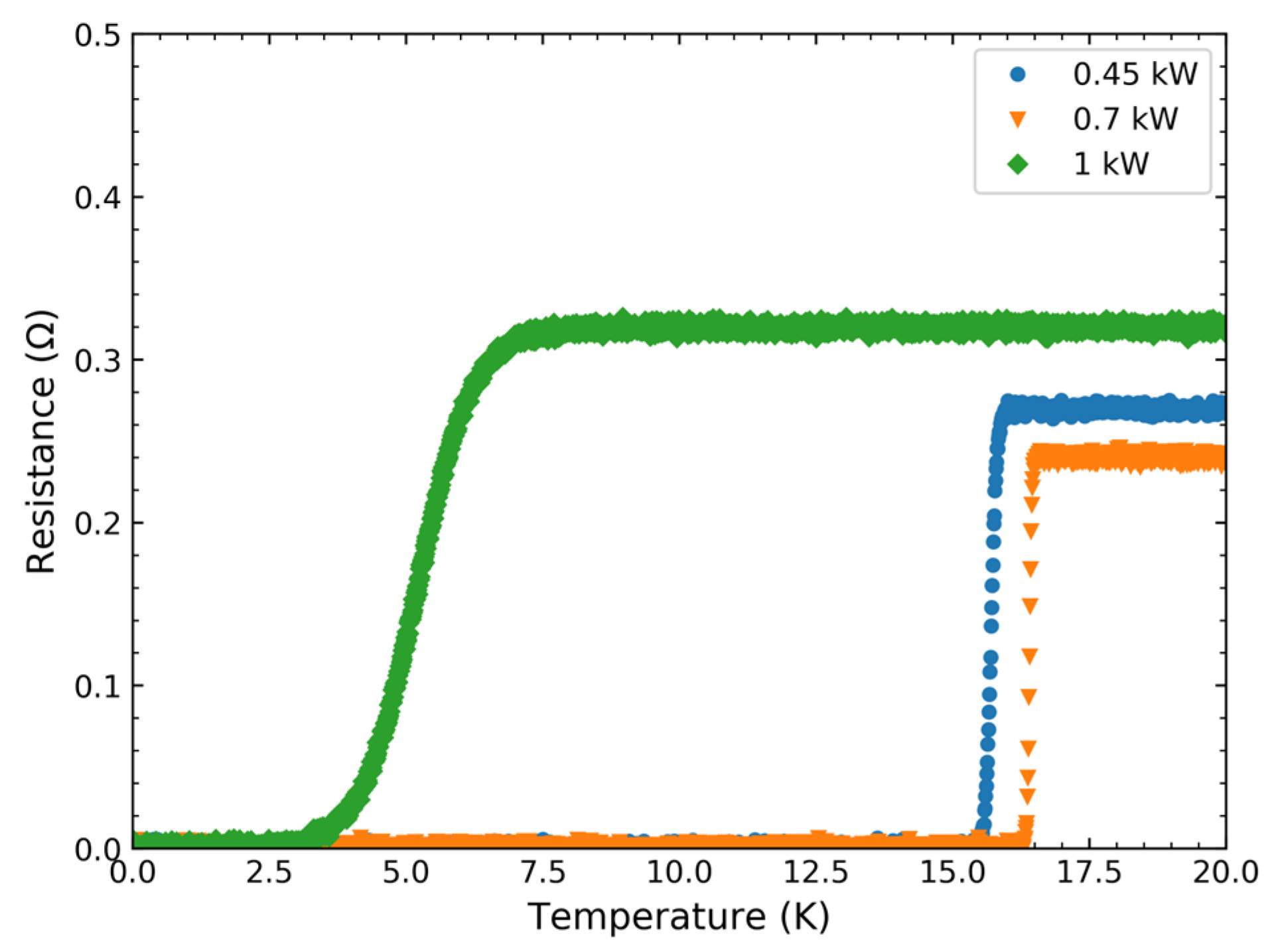
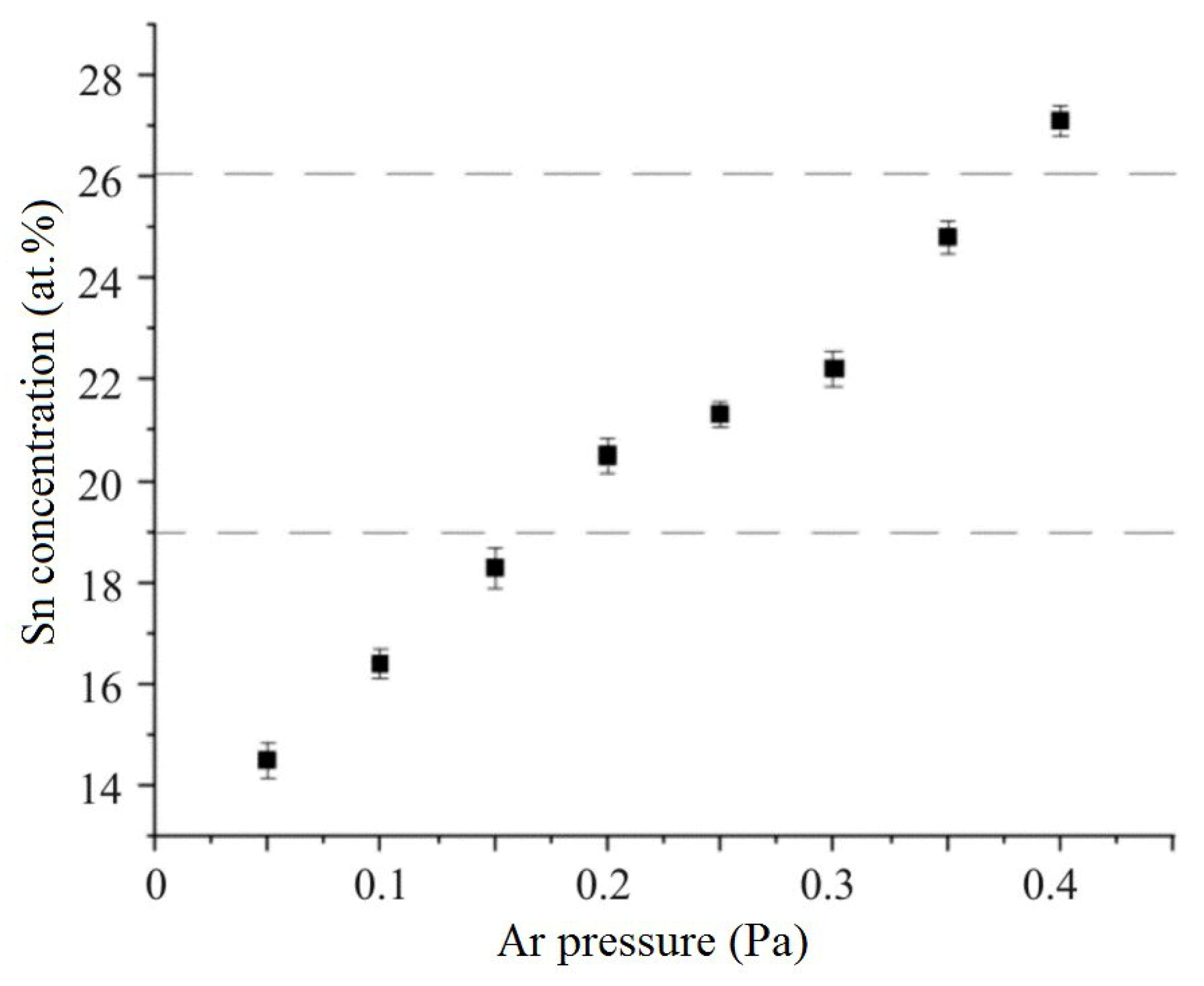
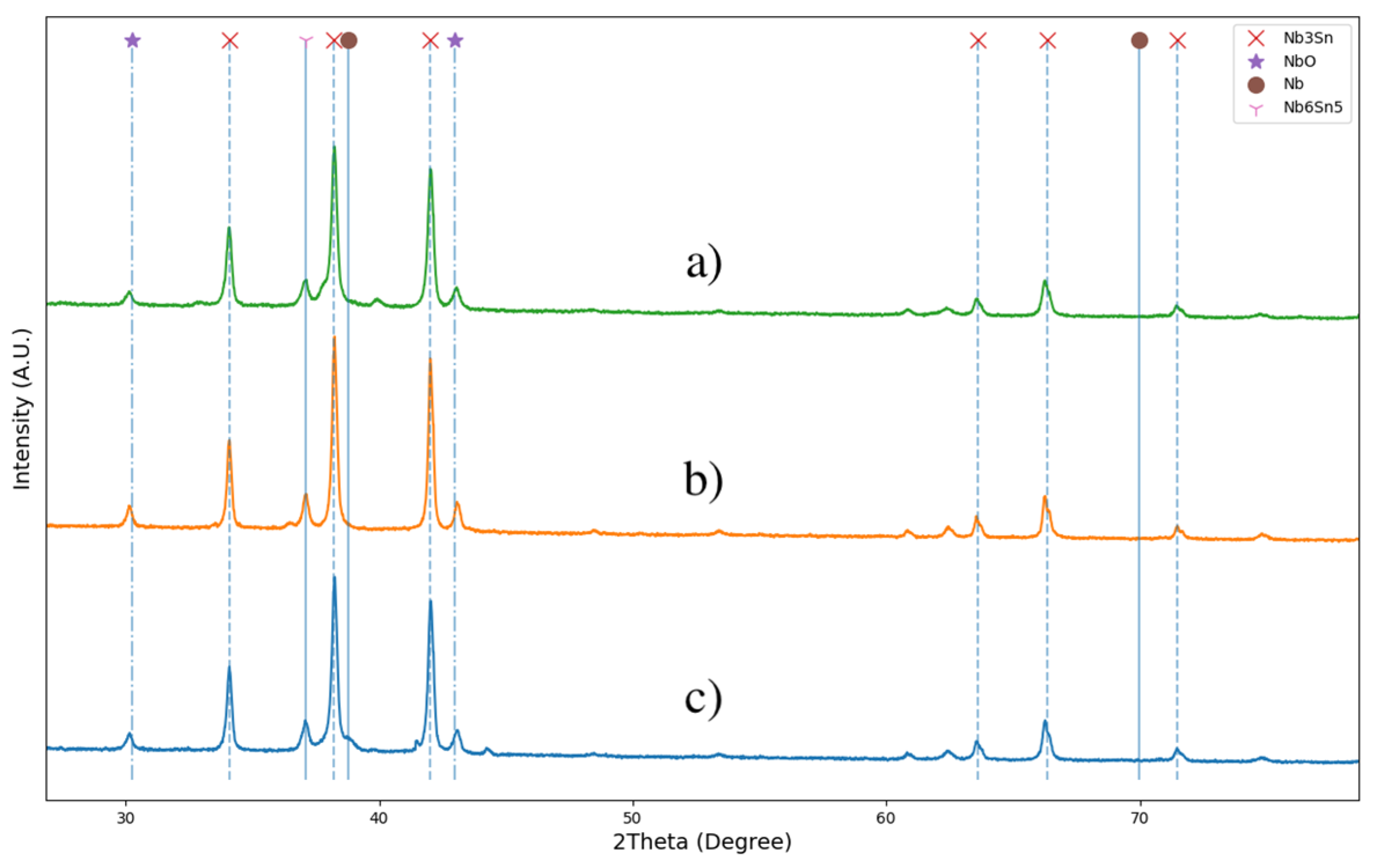
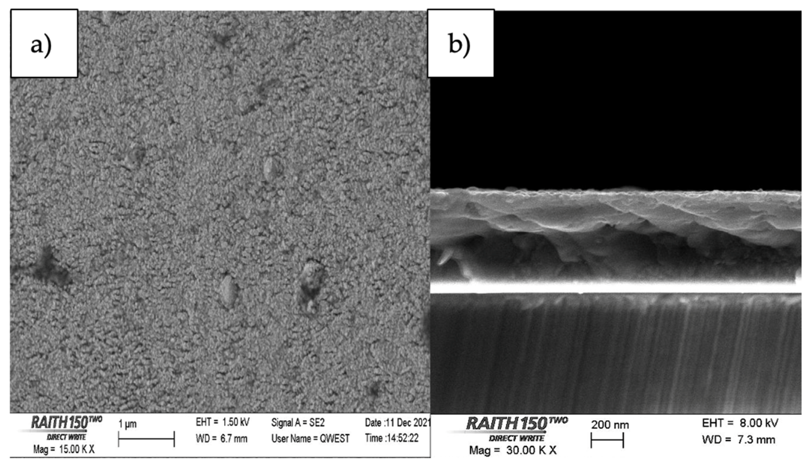
3. Results and Discussion

3.1. Co-Evaporation of Nb and Sn and Multilayer Coatings

It is known that the Nb3Sn phase is formed when the Sn content in the coating ranges from 19 to 26 at.%. In other ranges of the tin concentration, the formation of the undesirable phases Nb6Sn5 and NbSn2 is possible [14]. In order to obtain the required stoichiometric composition, a series of coating depositions at different magnetron discharge powers was carried out. The atomic Sn composition of the films deposited at different discharge powers was measured with EDS. The measurements were taken at five different locations for each film. The results of measuring the surface concentration of Sn in the coating (depending on the power of the magnetron M1) are shown in Figure 3.
As seen from the data, variations of the magnetron discharge power in the range of 0.45–0.7 kW resulted in a Sn surface concentration of the as-deposited coatings in the range of 19–24 at.%. The obtained concentrations correspond to the target values. For further research, the discharge power of M1 was chosen to be equal to 0.7 kW. Except for oxygen and trace carbon contents, no other impurities were found in the samples. At the same time, the layer-by-layer deposition mode was characterized by a high oxygen concentration (locally up to 20 at.%). More significant differences between the two deposition modes were revealed during the studies of the surface morphology and microstructure of the coatings.
Figure 4 shows the results of the studies of the surface (a) and the transverse cross-section (b) of the coating obtained with the simultaneous use of two magnetron sources. The surface of the coating is relatively smooth and homogeneous. The grain is clearly distinguishable on the transverse section, is quite large (700–900 nm), and has a clear orientation in the direction of the film growth.
The samples obtained by layer-by-layer deposition are characterized by an inhomogeneous structure and a rather fine grain with dimensions < 200–300 nm with no pronounced orientation (Figure 5a). The surface is rough, and the appearance of the surface indicates the formation of an oxide (Figure 5b).
In general, from the point of view of the properties of this type of coating in high-frequency fields, a larger grain is preferable [4]. In addition, despite a sufficiently high residual vacuum in the working chamber, it seems that Sn oxidation occurred during the deposition process, which prevented the formation of a homogeneous structure. This result also explains the large volume concentration of oxygen measured by energy dispersion spectroscopy.
For the formation of the target Nb3Sn phase, selected samples were subjected to high-temperature annealing in a vacuum furnace (at a temperature of 800 °C) since as-deposited Nb3Sn coatings do not demonstrate high critical temperatures [15]. Before and after the temperature exposure, the microstructure and phase composition of the samples were controlled using XRD.
The spectra after annealing are characterized by a pronounced structure with the presence of many reflexes, while the samples before annealing are characterized by the absence of reflexes, indicating an amorphous coating. In all modes at temperatures of 800 °C, the formation of the intermetallic Nb3Sn phase and the NbO phase occurred.
At the same time, for the sample obtained by multilayer deposition, the proportion of niobium oxide was significant, reaching a value of up to 25 vol.%. This result is also in qualitative agreement with the results of the elemental composition and microscopy studies. In general, an increased concentration of niobium oxide will not allow the formation of high superconducting properties for this type of coating. In addition, the presence of a large number of inclusions on the surface under conditions of high-frequency fields will lead to the formation of local field inhomogeneities, up to the loss of the superconducting state (“quenching”). Because of these considerations, more detailed studies with samples obtained using this processing mode were not carried out.
For the co-evaporated coatings, the XRD (Figure 6) analysis results indicate the presence of additional Nb6Sn5/NbSn2 phases at 1.0 kW (corresponding to a concentration of about 30 at.%). The coating samples obtained at a magnetron discharge power of 0.45 and 0.7 kW are characterized by high repeatability of the results and a relatively low volume fraction of NbO (up to 2–3% maximum).
Four-probe resistance measurements at liquid helium temperatures were carried out for all three modes of magnetron sputtering (Figure 7). For all samples, a transition to a superconducting state was observed. At the same time, the critical temperatures differed significantly. Thus, the worst results were demonstrated by a sample obtained at a magnetron discharge power of 1.0 kW–5.2 K. Significantly better results were obtained for a sample of 0.45 kW–15.7 K. It is obvious that the presence of non-superconducting Nb6Sn5/NbSn2 phases in the sample contributes to a decrease in the critical temperature value. The highest value of the critical temperature of 16.4 K was registered for a sample processed at a magnetron discharge power of 0.7 kW. This sample is characterized by a Sn content of 24 at.%, close to the “ideal” stoichiometric composition, and the lowest content of the NbO phase.
The results obtained qualitatively coincide with the results of the other measurements. The best results were obtained for samples with a low niobium oxide phase content, relatively high Sn content, large grains, and low surface roughness. Reducing the proportion of residual oxygen pollution can significantly improve the obtained results.

3.2. Deposition for a Stoichiometric Target

Similar to the experiments for Nb and Sn co-evaporation, in order to achieve the optimal conditions and desired target stoichiometry, a series of depositions were conducted. Coatings of Nb3Sn composite targets were sprayed at fixed parameters of the power supply. The discharge power was 0.5 kW, the pulse repetition rate was 100 kHz, and the fill factor was 70%. To control for the elemental composition, the pressure was varied (by the mean of the change in the Ar flow in the experimental chamber). The results of the experiments are shown in Figure 8.
From the above curve, the content of Sn in the coating strongly depends on the Ar pressure in the vacuum chamber. The measurement results using EDS indicate that the required Sn concentration is achieved in a pressure range of 0.2–0.35 Pa. Further studies, including annealing in a high-vacuum furnace, were carried out for samples obtained at pressure values in the specified range.
Before and after annealing of the samples, the phase composition was studied by XRD analysis. It is possible to identify some pattern characteristics of all of the analyzed samples. Firstly, all coatings before annealing are characterized by the presence of several diffraction peaks corresponding to Nb and Nb3Sn. The presence of a peak corresponding to pure niobium can be explained by the fact that deposition occurred on a “cold” substrate.
Secondly, the diffraction pattern changes drastically after high-temperature annealing. The spectra after annealing are characterized by a pronounced structure with the presence of many reflexes. Peaks of Nb3Sn and NbO are clearly distinguished in the entire pressure and temperature range. The peaks of the Nb3Sn have several pronounced orientations at (200), (210), (211), (320), (321), and (400).
The presence of reflexes corresponding to niobium oxide indicates, mainly, the oxidation of the target during high-temperature treatment. It is important to note that the volume content of oxide in the samples differs depending on the deposition mode. Thus, the lowest niobium oxide content of 4% is observed for a sample obtained at a pressure of 0.3 Pa and a corresponding tin concentration of about 23 at.%. The worst results were obtained for a sample at a pressure of 0.2 Pa—its volume content of the oxide exceeds 20%.
The sample obtained at a pressure of 0.35 Pa is also interesting. In terms of oxide content, the results are close to the 0.3 Pa sample. At the same time, the analysis indicates the presence of a peak of the Nb6Sn5 phase at 37.1° (Figure 9). The presence of this phase correlates with the measured tin content (about 25 at.%) and the phase diagram but is undesirable from the point of view of achieving high superconducting properties (for example, critical temperature). It can be assumed that local heterogeneities in the distribution of niobium and tin concentrations after deposition of the coating contribute to the formation of this phase. For a more detailed explanation of this phenomenon, it is necessary to carry out elemental mapping and examinations of samples using transmission electron microscopy (including the possibility of obtaining micro diffraction patterns).
Another interesting feature is related to the influence of the high-vacuum annealing temperature. At a temperature of 700 °C, as noted earlier, there are no reflexes corresponding to pure Nb. A further increase in temperature to 800 °C does not lead to a significant change in the XRD spectrum, but there is a slight increase in the intensity of the Nb3Sn peaks and a decrease in their FWHM, and, consequently, an increase in the volume fraction of the Nb3Sn.
A different picture is observed when analyzing images obtained at a temperature of 900 °C. There is a slight decrease in the volume content of Nb3Sn. In addition, a reflex corresponding to niobium is visible in one of the samples. This behavior, apparently, is associated with the beginning of the process of evaporation of Sn under long-term exposure to high temperatures. It can be expected that a further increase in temperature will lead to an increase in this effect and, thus, undesirable results.
The results of the studies of the surfaces and cross-sections by scanning electron microscopy and energy-dispersion spectroscopy also indicate several patterns. The grain is clearly distinguishable on the transverse section, is quite large, and has a clear orientation in the direction of the film growth. On the surface, in general, the grain is fine (about 150 nm). At the same time, the appearance of the surface indicates the presence of larger inclusions. Elemental analysis of such structures indicates an increased concentration of Sn (up to ~30 at.%), which can also negatively affect the uniformity of its superconducting properties for SRF applications.
The grain structure and concentration vary significantly depending on the processing mode. Thus, as the temperature increases to 800 °C, an increase in grain size is observed, as well as a slight decrease in the number of large clusters with an increased concentration of tin. A further increase to 900 °C leads both to the expected grain growth (which in theory should have a positive effect on the radio-frequency properties of the coating), and to an undesirable decrease in Sn concentration, along with the appearance of local structures (clusters) with a Sn content of less than 15%.
These results are in qualitative agreement with the data of the XRD analysis and indicate the undesirability of further increases in the annealing temperature. Figure 10 shows the typical appearance of the surface (a) and the cross section (b) for the coating obtained at a pressure of 0.3 Pa after annealing at a temperature of 800 °C.
Four-probe resistance measurements demonstrated the transition to a superconducting state at liquid helium temperatures for samples obtained under all three temperature conditions (samples at 0.3 Pa). At the same time, the highest value of 16.9 K was obtained for a sample processed at a temperature of 800 °C. An increase in the temperature to 900 °C led to a decrease in the critical temperature to 13.4 K. These results are qualitatively consistent with the results of microscopy, elemental, and X-ray structural analysis.
It can be concluded that it is impractical to further increase the processing temperature. It is possible to increase the critical temperature by further reducing the pressure and, hence, the oxygen contamination during the annealing. In addition, it is necessary to conduct additional studies of the effect of annealing time on the elemental and phase composition of the superconducting films.

4. Conclusions

In the current paper, we used several techniques to fabricate Nb3Sn coatings on sapphire substrates using magnetron discharge plasma. The techniques used were co-evaporation of Nb and Sn, their layer-by-layer deposition, and direct sputtering of a stoichiometric Nb3Sn target.
In the case of a dual magnetron system (Nb and Sn), the composition of the film was controlled by varying the magnetron discharge power. With a discharge power of 0.45–0.7 kW, we achieved 19–24 at.% surface concentration of Sn in the as-deposited film measured by EDS. None of the as-deposited films demonstrated a superconducting transition. In the case of a layer-by-layer deposition, in a given experimental condition, we observed significant oxygen contamination of the substrates and the presence of the NbO phase was confirmed by XRD. Therefore, these samples were excluded from further analysis. With the co-evaporation technique, we managed to produce films with a smooth and homogeneous surface. The film structure was clearly distinguishable and contained large grains (700–900 nm) with a pronounced orientation in the direction of the film growth. The highest critical temperature of 16.4 K was achieved for samples processed at a magnetron discharge power of 0.7 kW and further annealing in a vacuum furnace for 12 h at 800 °C. The film was characterized by a Sn content (24 at.%) close to the “ideal” stoichiometric composition and the lowest content of the NbO phase.
With the direct sputtering of a stoichiometric Nb3Sn target, the coating was deposited with a fixed magnetron discharge power of 0.5 kW. To vary the Sn fraction, the pressure in the vacuum chamber was adjusted in the range of 0.05–0.4 Pa. With an Ar pressure of 0.2–0.35 Pa, the achieved surface concentration was in the range of 21–24 at.%. After the annealing, XRD analysis revealed the formation of the peaks of Nb3Sn, with several pronounced orientations (200), (210), (211), (320), (321), and (400). The grains were clearly distinguishable on the transverse section, were quite large, and had a clear orientation in the direction of the film growth.
In the current studies, the highest value of the critical temperature of 16.9 K was achieved for a sample annealed at a temperature of 800 °C. A further increase to 900 °C resulted in a decrease of the Sn content, followed by a decrease of the superconducting transition temperature down to 13.4 K.
Therefore, with at least two techniques, we produced films with good superconducting properties that are potentially suitable for superconducting radio-frequency (SRF) cavities. However, the present study is not absolute, and while multiple annealing temperatures and deposition techniques are probed, significant effort should be directed toward further improvement of the experimental conditions to reduce the residual oxygen contamination and to test various annealing times and temperatures.

Author Contributions

Investigation, Y.Y.; Conceptualization, Y.Y. and A.S.; methodology, A.Y. and A.K. (Anastasiia Kharisova); software, A.K. (Anastasiia Kharisova); validation, Y.Y., A.S., A.Y. and A.K. (Artem Kazimirov); formal analysis, Y.Y.; investigation, A.S.; resources, Y.Y.; data curation, A.K. (Artem Kazimirov); writing—All authors have read and agreed to the published version of the manuscript.

Funding

This work was financially supported by Grant No. 21-12-00364 from the Russian Science Foundation.

Conflicts of Interest

The authors declare no conflict of interest.

References

  1. Posen, S.; Lee, J.; Seidman, D.N.; Romanenko, A.; Tennis, B.; Melnychuk, O.S.; Sergatskov, D.A. Advances in Nb3Sn superconducting radiofrequency cavities towards first practical accelerator applications. Supercond. Sci. Technol. 2021, 34, 025007. [Google Scholar] [CrossRef]
  2. Posen, S.; Hall, D.L. Nb3Sn superconducting radiofrequency cavities: Fabrication, results, properties, and prospects. Supercond. Sci. Technol. 2017, 30, 033004. [Google Scholar] [CrossRef]
  3. Pudasaini, U.; Eremeev, G.; Reece, C.E.; Tuggle, J.; Kelley, M. Initial growth of tin on niobium for vapor diffusion coating of Nb3Sn. Supercond. Sci. Technol. 2018, 32, 045008. [Google Scholar] [CrossRef]
  4. Tan, W.; Ma, R.; Pan, H.; Zhao, H.; He, X.; Chen, X.; Zhao, C.; Lu, X. The observation of tin islands in Nb3Sn thin films deposited by magnetron sputtering. Phys. C Supercond. Its Appl. 2020, 576, 1353667. [Google Scholar] [CrossRef]
  5. Xiao, L.; Lu, X.; Yang, Z.; Tan, W.; Yang, Y.; Zhu, L.; Xie, D. Annealing study on the properties of Cu-based Nb3Sn films under argon pressures for SRF applications. Phys. C Supercond. Its Appl. 2021, 586, 1353894. [Google Scholar] [CrossRef]
  6. Grassellino, A.; Romanenko, A.; Sergatskov, D.; Melnychuk, O.; Trenikhina, Y.; Crawford, A.; Rowe, A.; Wong, M.; Khabiboulline, T.; Barkov, F. Nitrogen and argon doping of niobium for superconducting radio frequency cavities: A pathway to highly efficient accelerating structures. Supercond. Sci. Technol. 2013, 26, 102001. [Google Scholar] [CrossRef]
  7. Sharma, R.G. Review on the fabrication techniques of A-15 superconductors. Cryogenics 1987, 27, 361–378. [Google Scholar] [CrossRef]
  8. Godeke, A. A review of the properties of Nb3Sn and their variation with A15 composition, morphology and strain state. Supercond. Sci. Technol. 2006, 19, R68. [Google Scholar] [CrossRef]
  9. Hillenbrand, B.; Martens, H.; Pfister, H.; Schnitzke, K.; Uzel, Y. Superconducting Nb3Sn cavities with high microwave qualities. IEEE Trans. Magn. 1977, 13, 378–491. [Google Scholar] [CrossRef]
  10. Sun, Z.; Ge, M.; Maniscalco, J.T.; Arrieta, V.; McNeal, S.R.; Liepe, M.U. Electrochemical Polishing of Chemical Vapor Deposited Niobium Thin Films. arXiv 2023, arXiv:2301.00788. [Google Scholar] [CrossRef]
  11. Agatsuma, K.; Tateishi, H.; Arai, K.; Saitoh, T.; Nakagawa, M. Nb3Sn thin films made by RF magnetron sputtering process with a reacted Nb3Sn powder target. IEEE Trans. Magn. 1996, 32, 2925–2928. [Google Scholar] [CrossRef]
  12. Kampwirth, R.; Hafstrom, J.; Wu, C. Application of high rate magnetron sputtering to the fabrication of A-15 compounds. IEEE Trans. Magn. 1977, 13, 315–318. [Google Scholar] [CrossRef]
  13. Sayeed, M.N.; Pudasaini, U.; Eremeev, G.V.; Elsayed-Ali, H.E. Fabrication of superconducting Nb3Sn film by Co-sputtering. Vacuum 2023, 212, 112019. [Google Scholar] [CrossRef]
  14. Ilyina, E.A.; Rosaz, G.; Descarrega, J.B.; Vollenberg, W.; Lunt, A.J.G.; Leaux, F.; Calatroni, S.; Venturini-Delsolaro, W.; Taborelli, M. Development of sputtered Nb3Sn films on copper substrates for superconducting radiofrequency applications. Supercond. Sci. Technol. 2019, 32, 035002. [Google Scholar] [CrossRef]
  15. Koblischka, M.R.; Pust, L.; Chang, C.-S.; Hauet, T.; Koblischka-Veneva, A. The Paramagnetic Meissner Effect (PME) in Metallic Superconductors. Metals 2023, 13, 1140. [Google Scholar] [CrossRef]
  16. Shakel, M.S.; Elsayed-Ali, H.E.; Eremeev, G.; Pudasaini, U.; Valente-Feliciano, A.M. First Results from Nb3Sn Coatings of 2.6 GHz Nb SRF Cavities Using DC Cylindrical Magnetron Sputtering System. arXiv 2023, arXiv:2307.08806. [Google Scholar]
  17. Deambrosis, S.M. 6 GHz Cavities: A Method to Test A15 Intermetallic Compounds Rf Properties; Universita Degli Studi di Padova: Padova, Italy, 2008. [Google Scholar]
  18. Allen, L.; Beasley, M.; Hammond, R.; Turneaure, J. RF surface resistance of high-Tcsuperconducting A15 thin films. IEEE Trans. Magn. 1983, 19, 1003–1006. [Google Scholar] [CrossRef]
  19. Carta, G.; Rossetto, G.; Zanella, P.; Crociani, L. Attempts to deposit Nb3Sn by MO-CVD. In Proceedings of the International Workshop on Thin Films and New Ideas for Pushing the Limits of RF Superconductivity, LNL, Legnaro, Italy, 9–12 October 2006. [Google Scholar]
  20. Rossi, A.A.; Deambrosis, S.M.; Stark, S. A15 Nb3Sn Films by Multilayer Sputtering & Review of SRF Tests. In Proceedings of the Proceedings of SRF 2009, Berlin, Germany, 20–25 September 2009; pp. 149–154. [Google Scholar]
  21. Le Febvrier, A.; Landalv, L.; Liersch, T.; Sandmark, D.; Sandstrom, P.; Eklund, P. An upgraded ultra-high vacuum magnetron-sputtering system for high-versatility and software-controlled deposition. Vacuum 2021, 187, 110137. [Google Scholar] [CrossRef]
  22. Sayeed, M.N.; Pudasaini, U.; Charles, E. Properties of Nb3Sn films fabricated by magnetron sputtering from a single target. Appl. Surf. Sci. 2021, 541, 148528. [Google Scholar] [CrossRef]
  23. Sayeed, M.N.; Eremeev, G.V.; Owen, P.; Reece, C.; Elsayed-Ali, H.E. Microstructural and superconducting radiofrequency properties of multilayer sequentially sputtered Nb3Sn films. IEEE Trans. Appl. Supercond. 2021, 31, 1–4. [Google Scholar] [CrossRef]
  24. Zhu, L.; Lu, X.; Yang, Z.; Tan, W.; Yang, Y.; Xiao, L.; Xie, D. Study on preparation of Nb3Sn films by bronze route. Phys. C Supercond. Its Appl. 2022, 601, 1354113. [Google Scholar] [CrossRef]
  25. Shakel, S.; Sayeed, N.; Eremeev, G.V.; Valente-Feliciano, A.-M.; Pudasaini, U.; Elsayed-Ali, H.E. Commissioning of a two-target DC cylindrical magnetron sputter coater for depositing Nb3Sn film on Nb superconducting radiofrequency cavities. Vacuum 2023, 217, 112563. [Google Scholar] [CrossRef]
  26. Vandenberg, J.; Gurvitch, M.; Hamm, R.; Hong, M.; Rowell, J. New phase formation and superconductivity in reactively diffused Nb3Sn multilayer films. IEEE Trans. Magn. 1985, 21, 819–822. [Google Scholar] [CrossRef]
  27. Xiao, L.; Lu, X.; Xie, D.; Tan, W.; Yang, Y.; Zhu, L. The Technical Study of Nb3Sn Film Deposition on Copper by HiPIMS. In Proceedings of the 19th International Conference on RF Superconductivity, SRF2019, Dresden, Germany, 30 June–5 July 2019; pp. 846–847. [Google Scholar]
  28. Sayeed, N.; Pudasaini, U.; Reece, C.E.; Eremeev, G.V.; Elsayed-Ali, H.E. Effect of substrate temperature on the growth of Nb3Sn film on Nb by multilayer sputtering. Thin Solid Film. 2022, 763, 139569. [Google Scholar] [CrossRef]
  29. Valizadeh, R.; Hannah, A.N.; Aliasghari, S.; Malyshev, O.B.; Stenning, G.B.G.; Turner, D.; Dawson, K.; Dahnak, V.R. PVD Deposition of Nb3Sn thin film on copper substrate from an alloy Nb3Sn target. In Proceedings of the IPAC’19, Melbourne, Australia, 19–24 May 2019; pp. 2818–2821. [Google Scholar]
  30. Aliasghari, S.; Avcu, E.; Skeldon, P.; Valizadeh, R.; Mingo, B. Abrasion resistance of a Nb3Sn magnetron-sputtered coating on copper substrates for radio frequency superconducting cavities. Mater. Des. 2023, 231, 112030. [Google Scholar] [CrossRef]
Figure 1. An external view of the experimental setup.
Metals 13 01730 g001
Figure 2. Typical temperature and pressure dependence during the high-temperature annealing.
Metals 13 01730 g002
Figure 3. Dependence of the Sn concentration in the coating on the magnetron power during layer-by-layer (multilayer) deposition using two magnetrons.
Metals 13 01730 g003
Figure 4. SEM images of the surface (a) and the cross-section (b) of the coating obtained by co-evaporation of Nb and Sn.
Metals 13 01730 g004
Figure 5. SEM images of the surface (a) and the cross-section (b) of the coating obtained by multilayer deposition of Nb and Sn.
Metals 13 01730 g005
Figure 6. XRD spectra of Nb–Sn thin films obtained after annealing: 1—coating obtained by layer-by-layer deposition of Nb and Sn; 2, 3—coatings obtained by co-evaporation.
Metals 13 01730 g006
Figure 7. Resistance versus temperature of co-evaporated Nb-Sn thin films obtained after 24 h of annealing at a temperature of 800 °C.
Metals 13 01730 g007
Figure 8. Dependence of the Sn concentration on the Ar pressure in the working chamber during the deposition of a coating for a composite target of Nb3Sn.
Metals 13 01730 g008
Figure 9. Results of the XRD analysis for images obtained during the deposition of a coating of a composite Nb3Sn target, demonstrating the formation of the Nb6Sn5 phase (0.35 Pa): (a) 700 °C, (b) 800 °C, (c) 900 °C.
Metals 13 01730 g009
Figure 10. SEM image of the surface (a) and cross-section (b) after the deposition of a coating of a Nb3Sn composite target (0.3 Pa) and annealing at a temperature of 800 °C.
Metals 13 01730 g010
Disclaimer/Publisher’s Note: The statements, opinions and data contained in all publications are solely those of the individual author(s) and contributor(s) and not of MDPI and/or the editor(s). MDPI and/or the editor(s) disclaim responsibility for any injury to people or property resulting from any ideas, methods, instructions or products referred to in the content.

