Abstract
The Silicon on Dust Substrate (SDS) is a gas-to-wafer process that produces multicrystalline silicon ribbons directly from gaseous feedstock (silane), avoiding the standard industry steps of polysilicon deposition, crystal growth, and wafering. The SDS technique consists of three main steps: (i) micrometric-sized silicon powder production by grinding silicon chunks; (ii) chemical vapor deposition (CVD) of silicon over this silicon powder substrate; and (iii) zone-melting recrystallization (ZMR) of the nanocrystalline pre-ribbon obtained in the CVD step. Several samples were produced by this technique. During CVD, mechanically self-sustained nanocrystalline pre-ribbons were grown over silicon powder substrates, with growth rates in the order of 50 µm/min. The ZMR process performance is substantially impacted by the pre-ribbon physical characteristics. The best and largest recrystallizations were achieved on pre-ribbons grown over powder substrates with smaller particle sizes, which also have lower substrate powder incorporation ratios. Multicrystalline silicon ribbons with crystalline areas as large as 2 × 4 cm2 were successfully produced. These areas have visible columnar crystal growth with crystal lengths up to 1 cm. The SDS ribbons’ measured resistivity confirmed the high powder content of the resulting material. The ability to produce solar cells on SDS multicrystalline silicon ribbons was demonstrated.
1. Introduction
In the last three decades, the photovoltaic (PV) market has progressed from the megawatt (MW) scale to the terawatt (TW) scale. This enormous growth of photovoltaic systems deployment was accompanied by a reduction in the cost of the PV energy by a factor of 100 [1], and in certain countries, PV energy is already the cheapest way to produce electricity [2]. The PV market is expected to grow in the coming decades due to demand growth and the necessary progressive decarbonization of energy production [3]. The PV market is mostly driven by crystalline silicon (c-Si) technologies that in the last decades have represented more than 90% of the installed capacity [4].
The reduction in the price of PV energy was achieved both by decreasing the PV systems’ production costs and by increasing their conversion efficiency.
One possible trajectory to reduce the cost of photovoltaic devices and consequently the cost of PV energy is the direct growth of silicon ribbons instead of the highly energetically intensive ingot growth.
We present here the Silicon on Dust Substrate (SDS) method, a gas-to-wafer process to produce multicrystalline silicon ribbons, based on atmospheric pressure, using low-temperature (<600 °C) chemical vapor deposition (CVD) of silicon on top of a silicon dust substrate, followed by a zone-melting recrystallization (ZMR).
For several decades, ZMR has been used to recrystallize and purify silicon and other materials [5,6]. To our knowledge, the best solar cell results achieved on silicon substrates obtained by zone-melting recrystallization were 16.0% at Mitsubishi Electric Corporation [7] and 13.5% at Fraunhofer ISE [8]. Moreover, Reber at al. reported on high-throughput ZMR performed at speeds as high as 350 mm/min [9].
The SDS method skips the stages of polysilicon deposition, crystal growth, and wafering that are present in the conventional methods to produce multicrystalline silicon, thus avoiding the considerable material losses inherent to the wafering process [10]. This method has the potential to significantly reduce the energy used to produce silicon photovoltaic substrates, a feature that can be particularly relevant in the present context of the Ukraine–Russia conflict and the inherent rising energy costs.
The proposed method also provides a pathway for silicon material reuse from manufacturing losses or end-of-life PV systems, supporting circular economy principles [11,12].
In previous studies, the SDS was thoroughly described, and several results were presented [13,14,15]. In the present manuscript, the impact of the powder substrate grain size on the recrystallization step is analyzed and the ability to produce solar cells on SDS substrates is demonstrated.
2. Materials and Methods
We describe here the use of the Silicon on Dust Substrate (SDS) to produce multicrystalline silicon ribbons to be used in photovoltaic applications; the produced ribbons were tested by manufacturing solar cells.
2.1. SDS Approach
The Silicon on Dust Substrate is a gas-to-wafer process, aiming to produce multicrystalline silicon ribbons directly from gaseous feedstock, bypassing the standard industry steps of polysilicon deposition, crystal growth, and wafering. Figure 1 presents the SDS process diagram compared with crystalline silicon wafer production for solar applications.
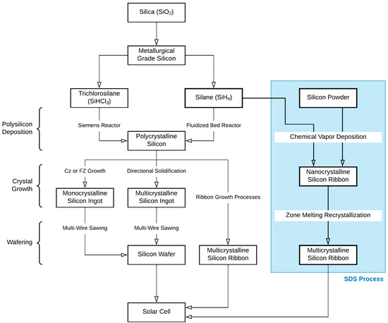
Figure 1.
Comparison between SDS and the crystalline silicon wafer industrial process. Note: Cz and FZ stand for Czochralski and Float Zone, respectively, the main growth methods to obtain monocrystalline silicon ingots.
The SDS technique consists of three main steps: (i) production of silicon powder; (ii) chemical vapor deposition (CVD) of silicon over a silicon powder substrate; and (iii) production of multicrystalline silicon ribbon by zone-melting recrystallization (ZMR) of the nanocrystalline pre-ribbon obtained in the CVD step.
The production of silicon powder is carried out in two stages: (a) silicon chunks are broken into small pieces using a wafer crusher with silicon-nitride-coated jaws; (b) the small pieces are then fed to a grinding mill, which produces the silicon powder. Any type of silicon material can be used as feedstock, but naturally the silicon powder obtained will retain the features of the original material.
In this study, the silicon chunks used as feedstock came from the remains of commercial multicrystalline p-type silicon samples with a resistivity between 0.5 and 1 Ω·cm.
The CVD step starts by placing a layer of silicon powder on top of a quartz holder, acting both as a deposition substrate during the CVD and as a sacrificial layer for easy detachment from the quartz. The silicon powder can also be obtained as a by-product of a fluidized bed reactor using silane as precursor. Next, a fast CVD at low temperature (<900 K) and atmospheric pressure, using silane as gaseous feedstock, deposits a thick layer of silicon over the powder substrate, resulting in a mechanically self-sustained, porous, and nanocrystalline silicon pre-ribbon. Finally, the pre-ribbon is subjected to ZMR, as a narrow horizontal floating molten zone with 2 mm height travels along the pre-ribbon and turns it into a multicrystalline silicon ribbon. Figure 2 shows a concise diagram of the SDS experimental process.
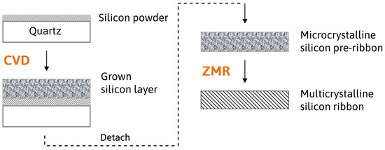
Figure 2.
SDS experimental process diagram.
The well-established production of silicon wafers, based on cutting either Czochralski-grown monocrystalline or directional-solidification-grown multicrystalline silicon ingots, using multi-wire sawing techniques, is responsible for global material losses rising to over 40% [1]; consequently, feedstock and wafering processes can represent up to one-third of the final cost of ingot-based silicon PV modules [16]. This situation justifies the research on alternative methods to produce silicon substrates that increase material yield and allow for further cost reductions of PV devices. Therefore, the SDS is part of a broader group of different approaches to the current PV industry standards that aims to increase the efficiency in material use, such as ribbon technologies [17,18], thin-films grown over a substrate [19,20,21], kerf-free wafering processes [22,23,24], and diamond-wire sawing followed by kerf recycling [25,26].
The SDS process is similar to several ribbon technologies in that it avoids the usual crystal growth methods, namely the use of a crucible and multi-wire sawing. However, some key differences set it apart from them: (i) in theory, SDS is a contamination-free process, since no foreign material is in contact with the silicon powder substrate during CVD or the floating molten silicon during ribbon recrystallization, which ensures that both gaseous feedstock and silicon powder have a high purity level; (ii) no high structural quality substrate is required; and (iii) it requires a low energy budget due to low temperature and atmospheric pressure used in the CVD process and due to the small volume of the molten zone during the ZMR process.
In summary, the SDS process has the potential to deliver good-quality material for solar cell manufacturing with a significant reduction in the overall cost.
2.2. Experimental Setup
The experimental setup used by the SDS process is composed of three main apparatuses: a grinding mill to deliver silicon powder of micrometric grain size [13], a CVD reactor to produce nanocrystalline pre-ribbons, and a zone-melting recrystallization furnace to finally obtain multicrystalline silicon ribbons. Both the grinding mill and CVD apparatuses are thoroughly described in previous works [13,14].
The current ZMR reactor is the fifth iteration of in-house developed reactors, built to perform zone-melting recrystallization in silicon ribbons using focused incoherent light as a heat source. The reactor is built of aluminum and composed of two parts: (i) the main body, measuring 220 × 140 × 76 mm3 and containing the optical system with two elliptical mirrors and two tubular halogen lamps of 1000 W each; (ii) the upper and lower chambers, which allow the vertical displacement of the recrystallizing ribbon and facilitate system cooldown. Silicon pre-ribbons from the CVD reactor, measuring up to 40 mm in width, can be recrystallized by a stable molten zone traveling at a speed in the range of 1 to 10 mm/min and under a controllable inner atmosphere. Figure 3a presents a simplified schematic of the reactor concept.
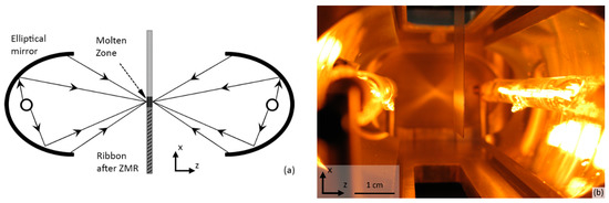
Figure 3.
ZMR reactor: (a) schematic of the concept and (b) close-up photo of the interior.
The recrystallization process was improved over past reactors, as the current optical system creates a stable and uniform molten zone, for up to 40 mm width (along the pre-ribbon length in the y direction) and 0.5 to 2.0 mm in height (x direction). Moreover, the reactor is airtight, making it possible to control the flow rate and gaseous species, which reduces the chance of contamination and oxidation. A close-up photo of the ZMR reactor’s interior is presented in Figure 3b, showing the optical system and a silicon pre-ribbon with focused radiation over the surface.
The optical system creates two heating regions at the same height on both sides of the silicon pre-ribbon surface, melting the entire ribbon material on a well-defined linear molten zone. The two mirrors have the same optical properties, with a focal distance of 30.6 mm and ellipse semi-axes of 39.9 mm and 25.5 mm. The 1000 W halogen lamps have a glass tubular encasement and an 80 mm long linear filament.
Each elliptical mirror has an effective focus angle of , resulting in a geometric efficiency of and a diffuse-to-focus power ratio of . The radiation intensity distribution over the pre-ribbon was computed with a ray-tracing software, and the following parameters were used: (i) the mirror surface is an aluminum-coated film, having an average reflection coefficient of 0.95 and no scattering; (ii) the reactor chamber material is unpolished aluminum with an average reflection coefficient of 0.60 and a gaussian scattering model; (iii) the number of analysis rays is 2 × 10⁶ for each lamp filament; and (iv) the target detector is a 60 × 30 mm rectangle with a 100% absorption rate placed in the same z axis position as the pre-ribbon. Figure 4 shows the ray-tracing simulation results obtained. Figure 4a presents the normalized radiation intensity map in the xy plane at the z coordinate where the pre-ribbon is placed. Figure 4b shows the normalized radiation intensity profile along the x coordinate at y = 0 (i.e., length of the ribbon), and Figure 4c shows the normalized radiation intensity profile along the y coordinate at x = 0 (i.e., width of the ribbon).
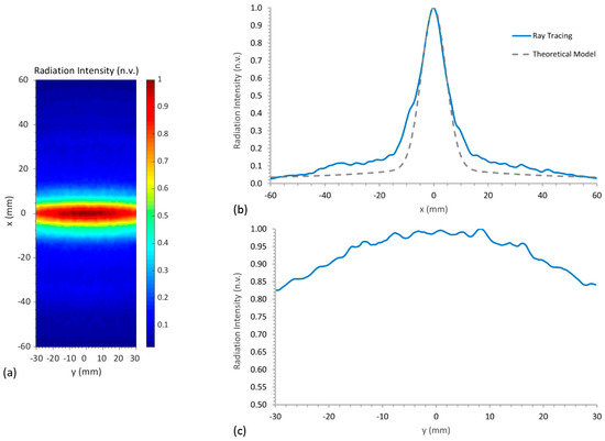
Figure 4.
Ray-tracing simulation of the radiation intensity over the recrystallized pre-ribbon (normalized): (a) xy plane intensity map; (b,c) profiles along the x and y directions.
It can be observed that the radiation is highly focused in a very thin strip that homogeneously covers the width of the pre-ribbon (y direction). Such a radiation profile explains the occurrence of a localized melting of silicon, which creates the molten zone.
2.3. Characterization
The characterization of the SDS ribbons consisted of the measurement of the thickness, before and after the ZMR step, followed by electrical measurements. The ribbons’ resistivity was measured with a four-point probe and the carrier lifetime was determined by microwave photoconductance decay (μ-PCD) measurements using a Semilab WT-1000. Finally, to further analyze the quality of ribbons, solar cells were produced and characterized by measuring one-sun I-V curve.
3. Results
The method of zone-melting recrystallization has been applied to several types of silicon substrates, both multicrystalline silicon wafers [26] and different kinds of silicon ribbons [14,27]. In addition, the ZMR method proved its ability to promote boron and phosphorous doping of silicon ribbons [28,29].
3.1. Pre-Ribbon Recrystallization
Obtaining recrystallized silicon samples, either ribbons or wafers, with a sufficiently low oxide content to be used in photovoltaic applications, depends on the occurrence of certain conditions. First, during the recrystallization, the partial pressure of oxygen on the furnace atmosphere should never exceed a threshold around 7% [26]. To ensure that this condition is met, it is important to consider that, despite the recrystallizations being performed in an argon atmosphere, there is possible contamination with ambient air. Furthermore, even if the samples are cleaned with an HF solution, their oxygen content will be released during recrystallization. The sample to be recrystallized must also meet two conditions: homogeneity and low porosity. It is harder to maintain a stable linear molten zone in a sample that does not have a homogeneous density and/or has a high level of porosity, where heat behavior is less predictable than in a homogenous and dense sample. Multicrystalline silicon wafers have relatively low oxygen content, and provided that the native oxide is removed by the HF cleaning, their recrystallization in an argon atmosphere is straightforward. On the other hand, the SDS pre-ribbons grown by CVD are more porous and less homogeneous, and the sample porosity also causes them to oxidize rapidly, which results in higher oxygen content than in the multicrystalline silicon wafers previously mentioned. Ribbons with such high oxygen content tend to form a film of silicon oxide in the heated areas of the ribbon during recrystallization. If not removed, the oxide layer will cover the molten zone, increasing the difficulty of monitoring and controlling it and often resulting in either an incomplete (or superficial) recrystallization or in a collapsed molten zone. Recrystallization of SDS ribbons is thus more complex; in fact, its complexity level strongly depends on the details of the CVD process, namely the grain size of the powder used as substrate.
The molten zone height can vary between 0.2 and 2.0 mm. The height attained depends not only on the lamp power applied and the focus accuracy of the optical system, but also on the sample properties and argon flux used. The appearance of the molten zone starts with the formation of one or more small silicon molten spots that rapidly spread laterally until a line-shaped molten zone (i.e., the linear molten zone) is formed. Initially its height is around 0.2–0.5 mm. After attaining a stable molten zone that spreads over the sample length (Figure 5), the molten zone height can be carefully increased up to 2.0 mm by a slight increase in the power applied to the halogen lamps.
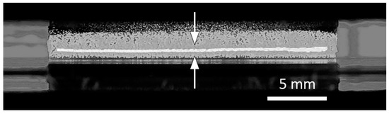
Figure 5.
Line-shaped molten zone in a CVD-grown pre-ribbon. The arrows point to the molten zone center.
3.2. SDS Pre-Ribbon Recrystallization and the Role of the Powder Grain Size
As previously mentioned, the properties of the pre-ribbon play an important role in the complexity and success level of the ZMR process. Figure 6 presents the images of three SDS ribbons after recrystallization. These ribbons differ mainly by the range of powder sizes used as substrate during the CVD process: (a) [106 µm, 180 µm]; (b) [75 µm, 106 µm]; (c) [45 µm, 75 µm].
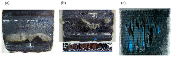
Figure 6.
SDS samples after ZMR: (a) [106 µm, 180 µm]; (b) [75 µm, 106 µm]; (c) [45 µm, 75 µm]. Note: Ribbon width is 25 mm.
In Figure 6a, an image of the ribbon grown with [106 µm, 180 µm] powder substrate is presented. It can be observed that during ZMR, soft oxide structures in the shape of thin filaments and hairy agglomerates are formed. In addition, several void areas are visible, which are due to molten zone collapse during recrystallization. To understand the reasons for this unsuccessful recrystallization, we must consider that the pre-ribbons obtained with such a large powder size have the highest powder incorporation ratio (~80%) between all the pre-ribbons obtained in this study [15]. A higher powder incorporation rate, which in fact corresponds to a lower incorporation of silicon from the gas phase, has two consequences for the ZMR process: (1) since the silicon from the gas phase deposits between the powder grains, gluing them together, a lower level of incorporation from gas will likely result in a less homogenous pre-ribbon; (2) the level of purity of the silicon powder is several orders of magnitude lower than the highly pure silicon deposited from the gas during CVD, and consequently a higher powder incorporation rate corresponds to a pre-ribbon with a higher contamination level. As previously mentioned, both these factors increase the level of complexity of the ZMR process.
When using substrates with lower grain sizes, the growth rate of the CVD process is higher (i.e., larger effective deposition area), originating from a higher incorporation of silicon from the gas phase and a lower powder incorporation ratio. As explained before, pre-ribbons with lower powder incorporation ratios will likely be more homogenous and have fewer impurities. The recrystallization of pre-ribbons grown using a [75 µm, 106 µm] powder substrate confirms this analysis, as can be observed in Figure 6b. Although the recrystallization of the pre-ribbon was challenging, with the formation of thick oxide layers in the silicon surface that hindered the success of the ZMR along large parts of the sample, in some small parts of the pre-ribbon it was possible to perform a complete recrystallization, obtaining elongated crystals with lengths up to 5 mm. For the pre-ribbon grown with the [45 µm, 75 µm] powder, the described trends are intensified: the CVD process has an even higher growth rate, and the powder incorporation ratio is reduced to 72%, resulting in a more homogenous pre-ribbon, potentially with a lower impurity content. Therefore, the recrystallization of this pre-ribbon was less eventful than the previous ones, and it was possible to successfully recrystallize an area of around 8 cm2, with elongated crystals with lengths up 1 cm visible on both sides of the ribbon, as can be observed in Figure 6c.
3.3. Characterization of SDS Ribbons
3.3.1. SDS Ribbon Thickness
The measurement of the ribbons’ thickness before and after recrystallization proved that there is a densification of samples during the ZMR step, resulting in thickness reductions between 40% and 60%, being larger for the samples grown with larger powder grain sizes. The ribbons’ thicknesses after recrystallization were in the 270–330 µm range.
3.3.2. Resistivity and Minority Carrier Lifetime Measurements
Table 1 presents the resistivity, average dopant concentration (ND), and carrier lifetime of an SDS ribbon.

Table 1.
Resistivity, dopant concentration, and carrier lifetime of SDS ribbon [14].
The bulk resistivity of the SDS Ribbons, measured using the four-point probe method, returned values around 0.70 Ω.cm, which corresponds to a doping level in the order of 2 × 1016 cm−3, the same doping level as the powder substrates used. This result further confirms the high powder incorporation rate of the ribbons. The SDS ribbons’ minority carrier lifetimes obtained by μ-PCD measurements were around 0.5 μs, which shows that the material obtained does not have enough quality to be used as a substrate for commercial solar cells. The low quality of the SDS ribbons can be attributed to the contamination of the silicon powder substrates with metallic impurities, such as iron. Such impurities, when incorporated in the multicrystalline silicon ribbons, act as recombination centers and limit the charge carrier lifetime [30].
3.3.3. Solar Cell Manufacture and Characterization
To further characterize the SDS ribbons, we produced solar cells on SDS substrates. Since the main goal was to compare the quality of the SDS ribbons obtained with commercial multicrystalline silicon wafers, the solar process was very simple: it consisted of the creation of the emitter (i.e., pn junction definition) and the metallic contacts’ formation. The solar cell emitter was produced by performing a phosphorous diffusion at a temperature of 900 °C. The metallic contacts were obtained in an evaporator: aluminum was used as back contact, and successive layers of titanium, palladium, and silver were evaporated to form the front contact. No anti-reflective coating, surface passivation, or back surface field were used; hence, one would not expect to attain high efficiencies. Still, SDS solar cells showed much lower efficiencies than the control cells made on commercial multicrystalline silicon wafers.
The solar cells obtained were characterized by measuring the one-sun I-V curve, and the solar cell parameters were obtained. In Figure 7, the I-V curve for the best SDS cell is presented.
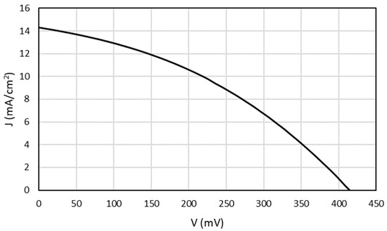
Figure 7.
I-V curve of the best SDS solar cell.
The main solar cell parameters for the best solar cells of each group are presented in Table 2.
Table 2.
Solar cell parameters of the best SDS and control solar cells.
As previously mentioned, solar cell processing is not optimized, which explains the overall low performance of the produced cells. The fill factor (FF) values are particularly low due to the lack of optimization of solar cell contacts, which caused important resistance losses. Regarding this aspect, the difference between SDS and control cells is not substantial. On the other hand, the SDS solar cell has, respectively, 29% and 26% losses in the open-circuit voltage (Voc) and short-circuit current density (Jsc), when compared to the control. Consequently, the best SDS solar cell attained an efficiency of 2.2% compared to 5.0% for the best control cell, which confirms the limited quality of the material obtained.
4. Discussion
The SDS process starts with the production of silicon powder. As previously mentioned, any type of silicon material can be used as feedstock, but in fact, the use of silicon with a high impurity level can compromise the growth process and quality of the ribbons obtained. Since the main goal of this study was to analyze the feasibility of the recrystallization of pre-ribbons grown by CVD over powder substrates with variable grain sizes, the purity level of the feedstock was not monitored, which explains the poor quality of the material obtained (i.e., low minority charge carrier lifetimes) and low performance of the solar cells produced. To achieve a better quality of the SDS ribbons, one must ensure that the metallic impurity level of the powder substrate is negligible.
It was observed that the success of the SDS process and the crystalline quality of the ribbons obtained are highly dependent on the size of the grain powder used as substrate during the CVD process. For larger powder grain sizes, the ZMR step is more eventful, with a lower success rate. For smaller powder grain sizes, ZMR is easier to perform, and for instance, using pre-ribbons grown on [45 µm, 75 µm] powder, crystalline areas as large as 8 cm2 were obtained.
All the SDS silicon ribbons produced have high powder incorporation rates (70–80%). Such high incorporation rates make the quality and features of the SDS ribbons highly dependent on the characteristics of the silicon powder. Hence, if a less pure silicon feedstock is used to produce the silicon powder, the resulting SDS ribbon will have a similar level of purity. Moreover, the feedstock doping level and type will largely determine the SDS ribbon doping level. Thus, it would be desirable to achieve a lower powder incorporation. On one hand, it is much easier to ensure the high purity of the gaseous source than of the powder. On the other hand, ribbons with a higher incorporation of silicon from the gaseous source tend to have a lower porosity [22], which strongly contributes to the success of the growth process and the quality of the SDS ribbons.
One possible way to reduce powder incorporation and ribbon porosity is to use a fixed amount of silicon powder as substrate and mechanically compact it at a fixed pressure around 100 MPa, four orders of magnitude higher than the manual compacting performed in this study.
Regardless of the SDS ribbons’ powder incorporation ratio, it is essential to ensure a higher purity of the silicon powders used as substrates to reduce the charge recombination in the silicon ribbon, as it compromises the quality of the solar cells produced.
5. Conclusions
The study presented here demonstrated the feasibility of the SDS process as a path to produce silicon ribbons for photovoltaic applications, avoiding the costly steps of ingot growth and wafering. The study also highlighted the importance of the features of the powder used as substrate during the CVD step, in particular its grain size: for pre-ribbons grown on powders with lower grain sizes, the ZMR step is easier to perform, the ribbons obtained have higher crystalline quality, and they can be used as substrates to produce solar cells.
As future developments, we suggest a better control of the quality of silicon powder used in the CVD step and achieving a lower powder incorporation ratio in the ribbons. Improved control of these two features will favor more straightforward zone-melting recrystallizations and the production of SDS ribbons with higher crystalline quality (i.e., larger crystal grains).
The SDS method can produce multicrystalline silicon ribbons for photovoltaic applications in a cost-effective way and has the potential to reduce the energy bill of photovoltaic systems. This is particularly relevant in the context of the present energy crisis. Additionally, the use of silicon chunks as a base material for the SDS process offers an opportunity to reuse manufacturing waste material or material from end-of-life PV systems, contributing to the increase in the circularity of the crystalline silicon PV industry.
Author Contributions
Conceptualization, F.S., J.A.S. and J.M.S.; methodology, F.S, J.A.S. and J.M.S.; software, F.S.; validation, formal analysis, investigation, F.S., I.C., J.A.S. and J.M.S.; resources and data curation, F.S. and I.C.; writing—original draft preparation, F.S. and J.A.S.; writing—review and editing, I.C. and J.M.S.; supervision, J.A.S. and J.M.S.; project administration and funding acquisition, J.M.S. All authors have read and agreed to the published version of the manuscript.
Funding
This research was funded by the Portuguese Fundação para a Ciência e a Tecnologia (FCT), through the grant number SFRH/BD/51377/2011 and through the project UIDB/50019/2020—IDL.
Institutional Review Board Statement
Not applicable.
Informed Consent Statement
Not applicable.
Data Availability Statement
Data will be made available on demand.
Conflicts of Interest
The authors declare no conflict of interest.
References
- ITRPV. International Technology Roadmap for Photovoltaic. 2022. Available online: https://www.vdma.org/international-technology-roadmap-photovoltaic (accessed on 15 December 2022).
- Kost, C.; Shammugam, S.; Fluri, V.; Peper, D.; Memar, A.D.; Schlegl, T. Levelized Cost of Electricity Renewable Energy Technologies. 2021. Available online: https://www.ise.fraunhofer.de/content/dam/ise/en/documents/publications/studies/EN2021_Fraunhofer-ISE_LCOE_Renewable_Energy_Technologies.pdf (accessed on 15 December 2022).
- International Energy Agency. World Energy Outlook 2019; International Energy Agency: Paris, France, 2019. [Google Scholar]
- Philipps, S.; Warmuth, W. Fraunhofer ISE: Photovoltaics Report; Fraunhofer ISE: Freiburg, Germany, 2022. [Google Scholar]
- Pfann, W.G. Techniques of zone melting and crystal growing. Solid State Phys. 1957, 4, 423–521. [Google Scholar]
- Pfann, W.G.; Theuerer, H.C. Applications of zone melting to analytical chemistry. Anal. Chem. 1960, 32, 1574–1578. [Google Scholar] [CrossRef]
- Ishihara, T.; Arimoto, S.; Morikawa, H.; Nishimoto, Y.; Kawama, Y.; Takami, A.; Hamamoto, S.; Naomoto, H.; Namba, K. Development of High Efficiency Thin Film Polycrystalline Silicon Solar Cells Using VEST Process. MRS Online Proc. Libr. 1997, 485, 3–11. [Google Scholar] [CrossRef]
- Kieliba, T.; Pohl, J.; Eyer, A.; Schmiga, C. Optimization of c-Si Films Formed by Zone-Melting Recrystallization for Thin-Film Solar Cells. In Proceedings of the 3rd World Conference on Photovoltaic Solar Energy Conversion, Osaka, Japan, 11–18 May 2003; p. 1170. [Google Scholar]
- Reber, S.; Eyer, A.; Haas, F. High-throughput zone-melting recrystallization for crystalline silicon thin-film solar cells. J. Cryst. Growth 2006, 287, 391–396. [Google Scholar] [CrossRef]
- Radhakrishnan, H.S.; Cho, J.; Bearda, T.; Roeth, J.; Depauw, V.; Van Nieuwenhuysen, K.; Gordon, I.; Szlufcik, J.; Poortmans, J. Freestanding and supported processing of sub-70 μm kerfless epitaxial Si and thinned Cz/FZ Si foils into solar cells: An overview of recent progress and challenges. Sol. Energy Mater. Sol. Cells 2019, 203, 110108. [Google Scholar] [CrossRef]
- Contreras-Lisperguer, R.; Muñoz-Cerón, E.; Aguilera, J.; de la Casa, J. A set of principles for applying Circular Economy to the PV industry: Modeling a closed-loop material cycle system for crystalline photovoltaic panels. Sustain. Prod. Consum. 2021, 28, 164–179. [Google Scholar] [CrossRef]
- Powell, D.M. Crystalline silicon photovoltaics: A cost analysis framework for determining technology pathways to reach baseload electricity costs. Energy Environ. Sci. 2012, 5, 5874–5883. [Google Scholar] [CrossRef]
- Augusto, A. Study of a Process to Grow Silicon Ribbons by Fast CVD. Ph.D. Thesis, Faculty of Sciences, University of Lisbon, Lisboa, Portugal, 2012. [Google Scholar]
- Serra, F.; Amar, E.; Pera, D.R.; Silva, J.A.; Serra, J.M. Zone melting recrystallization of microcrystalline silicon ribbons obtained by chemical vapor deposition. AIP Conf. Proc. 2019, 2147, 140008. [Google Scholar]
- Serra, F. Multicrystalline Silicon Ribbons Grown over a Dust Substrate. Ph.D. Thesis, Faculty of Sciences, University of Lisbon, Lisboa, Portugal, 2021. [Google Scholar]
- Kalejs, J.P. Silicon ribbons and foils—State of the art. Sol. Energy Mater. Sol. Cells 2002, 72, 139–153. [Google Scholar] [CrossRef]
- Hahn, G.; Schönecker, A. New crystalline silicon ribbon materials for photovoltaics. J. Phys. Condens. Matter 2004, 16, R1615–R1648. [Google Scholar] [CrossRef]
- Green, M.A. Thin-film solar cells: Review of materials, technologies and commercial status. J. Mater. Sci. Mater. Electron. 2007, 18, 15–19. [Google Scholar] [CrossRef]
- Jäger-Waldau, A. Status of thin film solar cells in research, production and the market. Sol. Energy 2004, 77, 667–678. [Google Scholar] [CrossRef]
- Schmich, E.; Schillinger, N.; Reber, S. Silicon CVD deposition for low-cost applications in photovoltaics. Surf. Coat. Technol. 2007, 201, 9325–9329. [Google Scholar] [CrossRef]
- Henley, F.J. Kerf-Free Wafering: Technology Overview and Challenges for Thin PV Manufacturing. In Proceedings of the 35th IEEE Photovoltaic Specialists Conference, Honolulu, HI, USA, 20–25 June 2010; pp. 001184–001192. [Google Scholar]
- Niepelt, R.; Hensen, J.; Steckenreiter, V.; Brendel, R.; Kajari-Schöder, S. Kerfless exfoliated thin crystalline Si wafers with Al metallization layers for solar cells. J. Mater. Res. 2015, 30, 3227–3240. [Google Scholar] [CrossRef]
- Bellanger, P.; Slaoui, A.; Minj, A.; Martini, R.; Debucquoy, M.; Serra, J.M. First Solar Cells on Exfoliated Silicon Foils Obtained at Room Temperature by the SLIM-Cut Technique Using an Epoxy Layer. IEEE J. Photovolt. 2016, 6, 1115–1122. [Google Scholar] [CrossRef]
- Kumar, A.; Melkote, S.N. Diamond Wire Sawing of Solar Silicon Wafers: A Sustainable Manufacturing Alternative to Loose Abrasive Slurry Sawing. Procedia Manuf. 2018, 21, 549–566. [Google Scholar] [CrossRef]
- Tomono, K.; Miyamoto, S.; Ogawa, T.; Furuya, H.; Okamura, Y.; Yoshimoto, M.; Komatsu, R.; Nakayama, M. Recycling of kerf loss silicon derived from diamond-wire saw cutting process by chemical approach. Sep. Purif. Technol. 2013, 120, 304–309. [Google Scholar] [CrossRef]
- Serra, J.M. Estudo de um Processo de Preparação de Fitas de Silício para Aplicação Fotovoltaica. Ph.D. Thesis, Faculty of Sciences, University of Lisbon, Lisboa, Portugal, 1995. [Google Scholar]
- Bellanger, P.; Sow, A.; Grau, M.; Augusto, A.; Serra, J.M.; Kaminski, A.; Dubois, S.; Straboni, A. New method of fabricating silicon wafer for the photovoltaic application based on sintering and recrystallization steps. J. Cryst. Growth 2012, 359, 92–98. [Google Scholar] [CrossRef]
- Silva, J.A.; Brito, M.C.; Costa, I.; Alves, J.M.; Serra, J.M.; Vallêra, A.M. Sprayed boric acid as a dopant source for silicon ribbons. Sol. Energy Mater. Sol. Cells 2007, 91, 1948–1953. [Google Scholar] [CrossRef]
- Silva, J.A.; Platte, B.; Brito, M.C.; Serra, J.M. New doping method to obtain n-type silicon ribbons. J. Cryst. Growth 2015, 428, 29–34. [Google Scholar]
- Dubois, S.; Palais, O.; Ribeyron, P.J.; Enjalbert, N.; Pasquinelli, M.; Martinuzzi, S. Effect of intentional bulk contamination with iron on multicrystalline silicon solar cell properties. J. Appl. Phys. 2007, 102, 083525. [Google Scholar] [CrossRef]


Disclaimer/Publisher’s Note: The statements, opinions and data contained in all publications are solely those of the individual author(s) and contributor(s) and not of MDPI and/or the editor(s). MDPI and/or the editor(s) disclaim responsibility for any injury to people or property resulting from any ideas, methods, instructions or products referred to in the content. |
© 2023 by the authors. Licensee MDPI, Basel, Switzerland. This article is an open access article distributed under the terms and conditions of the Creative Commons Attribution (CC BY) license (https://creativecommons.org/licenses/by/4.0/).