Article

In Situ Study the Grooving Effect Induced by Ag Particles on Rapid Growth of Cu6Sn5 Grain at Sn-xAg/Cu Soldering Interface during the Heat Preservation Stage

1
Physics Science and Engineering Technology College, Yichun University, Yichun 336000, China
2
School of Materials Science and Engineering, Dalian University of Technology, Dalian 116024, China
3
Faculty of Mechanical Engineering, Silesian University of Technology, Konarskiego 18A, 44-100 Gliwice, Poland
*
Authors to whom correspondence should be addressed.
Metals 2023, 13(8), 1445; https://doi.org/10.3390/met13081445
Submission received: 28 June 2023 / Revised: 1 August 2023 / Accepted: 3 August 2023 / Published: 11 August 2023

Abstract

:
Synchrotron radiation X-ray imaging technique was applied for in situ observation of Cu6Sn5 intermetallic compounds (IMC) growth in Sn/Cu and Sn-3.5Ag/Cu joints under isothermal temperature conditions of 250/300/350 °C and time duration of 1.5 h. The IMC in Sn-Ag solder was characterized by the formation of grooves during the interfacial reaction, and this can be attributed to the Ag content. Kinetically, the growth rate constants for the height of Cu6Sn5 were observed to increase with temperatures and the presence of Ag in solder. As compared to pure Sn solders, the Sn-3.5Ag solders were observed with interfacial IMC of greater height, smaller base width, and lowered aspect ratio.

1. Introduce

In electronic packaging industries [1], Pb-free Sn-Ag solders have been widely utilized for chip joint processing during the manufacturing of cheaper large-volume consumer products owing to their reasonable costs, good soldering performance, superior mechanical properties, as well as high resistance to thermal fatigue [2,3]. One of the notable reliability challenges in the context of lead-free Sn-based solder alloys is the formation of brittle intermetallic compounds (IMCs) [3,4,5,6,7,8]. The formation of Cu6Sn5 IMCs in Sn/Cu, Sn-Ag/Cu, and Sn-Ag-Cu/Cu during reflow soldering is mainly governed by the grain boundary diffusion of Cu into the solder, and this is again influenced by the interfacial grain orientation or Ag3Sn nano-particles in cooling stage [2,9,10,11,12,13]. Moreover, the solidified precipitated Ag3Sn phase is observed to only distribute on both sides of the groove boundary between adjacent grains, but not the entire grain surface from the SEM figures [2], from which can be inferred that Ag-free atoms are mainly distributed on the groove edges of the grains during the heat preservation stage. In our previous works, we also realized that competitive growth of Ag3Sn was only found in the early stage of the solidification process, and most of Ag3Sn was dissolved, and only some of them could grow up to the end [2,3]. Thus, the interfacial microstructure during the isothermal reflow heating is very crucial in the determination of overall IMC growth behavior. Many scholars consider soldering as a whole process to aimed at understanding the effects of Ag addition (or Ag concentration) on IMC growth, which cannot sufficiently explain the Cu6Sn5 microstructure solely during reflow soldering as the measurements results consist of the large number of IMCs precipitated at the interface during the cooling stage. Guo and Yang et al. [2,9], have utilized high pressure air gun to blow the liquid Sn, Sn-Ag, Sn-Ag-Cu solder away from the interface above the Cu substrate after a desired time duration of reflow soldering in order to avoid the cooling effects and mimic the growth of IMC at constant temperature [14]. Since the characterization method in their experiment was ex situ, it is difficult to predict the exact point of time grooving starts for different values of temperature. Moreover, ex situ sample characterization using high-pressure air and cross-section etching or polishing involves deviation and destruction effects on the resultant IMC size and morphology, which then leads to dimensional errors, and thus, this method cannot be utilized alone to generate thickness data for Cu6Sn5 compound formed at the interface [15].
In order to find the solution to these limitations, the synchrotron radiation-based real-time X-ray imaging experiments and high-pressure air method have been both utilized in this present study to in situ and ex situ observe the grooving effects of Ag particles on aspect ratio evolution of Cu6Sn5 grain at liquid-solder (L-S) interface of Sn-Ag/Cu joints at different temperatures during the heat preservation stage.

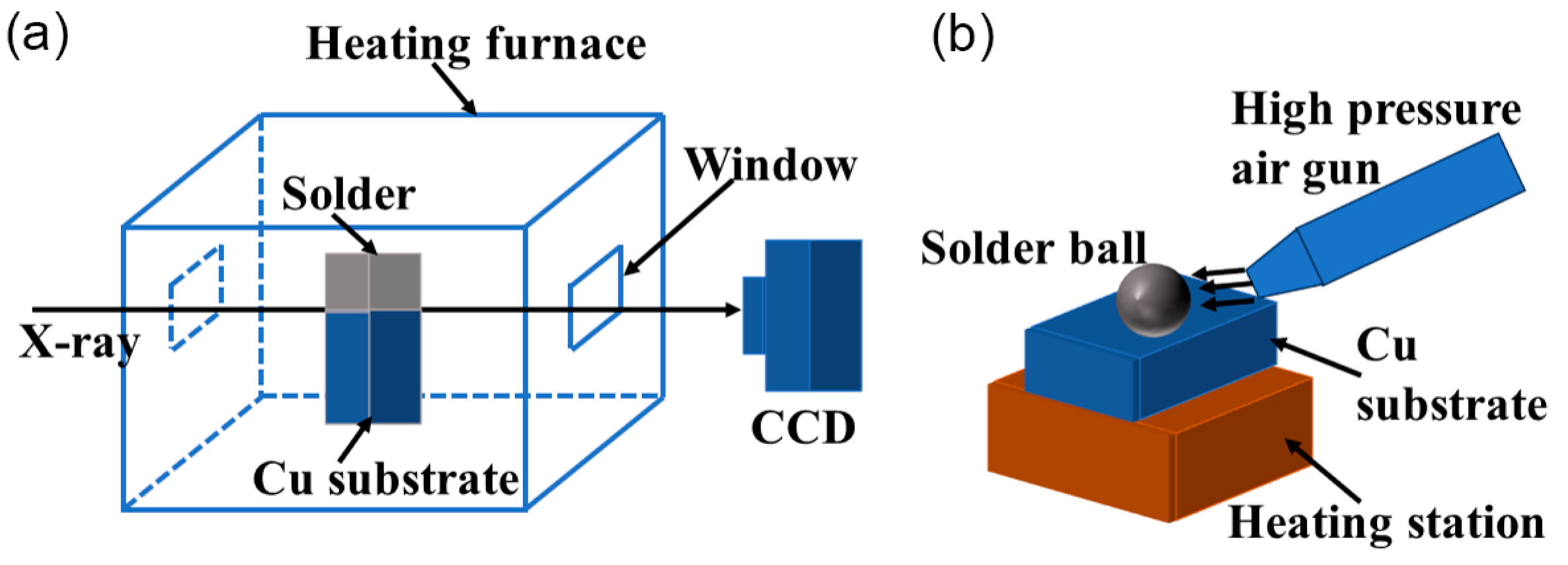
2. Experiment and Methods

The solder compositions chosen for this experiment are Sn-1Ag, Sn-3.5Ag solders, where the Pure Sn (Dalian Golden Saddle Welding Limited Company, Dalian, China; purity: 99.99%, Melting point: 231.89 °C) and Ag (Qingyuan Metal Materials Limited Company, Qingyuan, China; purity: 99.95%, Melting point: 961.78 °C) were mixed in accordance with the corresponding mass percentage (wt.%) and then put into a vacuum tube furnace. The temperature is raised to 500 °C in presence of argon atmosphere and kept for 5h to ensure that the ingredients are mixed uniformly and then cooled to room temperature within the furnace. The Sn and Sn-xAg (x = 1, 3.5) solders are rolled into thin sheets and melted on titanium foil, forming solder balls with diameters of 1 mm in a tin melting furnace. Finally, the preparation for soldering was finished after washing the solder balls with acetone and alcohol.
The situ experiment was carried out using the BL13W1 beamline [16] of Shanghai synchrotron radiation facility (SSRF), Shanghai, China. The energy of monochromatic beam was selected as 23 Kev. A charged couple device (CCD) camera was used to capture the images, with an image size of 2048 pixels × 2048 pixels, resolution ratio of 0.325 μm/pixel, and time interval of 4s per frame. Pure Sn (99.95% pure), Sn-3.5Ag, and polycrystalline Cu (99.95% pure) were used as soldering materials. Figure 1a shows the schematic diagram of experimental setup for in situ observations. The Cu sheet size was chosen as 20 mm × 5 mm × 0.1 mm, and solder size was taken as 10 mm × 5 mm ×0.1 mm. The soldering experiment was carried out in a furnace at three constant soldering temperature values of 250/300/350 °C, and the furnace heating was turned off after 1.5 h. Thus, the start time of the experiment is taken as the point when the system reaches and stabilizes in the set temperature value by precision temperature control cabinet. Shanghai synchrotron radiation (SR) facility was applied to characterize the microstructure of interfacial IMCs. For reliability study, the SR images were used to determine the IMC thicknesses by the following mathematical formula [10]:
H IMC = H SR × N IMC N SR
where H IMC is the mean thickness of IMC layers, H SR is the actual height of the SR image, and N IMC and N SR are the number of pixels in the IMC layers and the entire SR image, respectively. The SR images (2048 pixel × 2048 pixel) covering numerous grains in the interface were analyzed for each sample.
In context of observing top-section and cross-section views of intermetallics compounds via ex situ scanning electron microscopy (SEM) method, the pure Sn (99.99%), Sn-1Ag, Sn-3.5Ag solders with a diameter of 1mm solder balls are used to react with polycrystalline Cu substrate (Qingyuan Metal Materials Limited Company, Qingyuan, China; purity: 99.99%, melting point: 1083.4 °C, the size: 2000 μm × 2000 μm × 100 μm) substrate in the reflow furnace at 250 °C, 275 °C, 300 °C with reaction time being 30 s, 60 s, 120 s. Then, the samples are cooled by high-pressure air as ex situ samples (Figure 1b). Two kinds of cooling samples are prepared for SEM by grinding, polishing, and etching with 5% HNO3 + 2%HCl + 93%C2H5OH (in volume) solution to reveal the cross-sectional morphology. Similarly, some samples were etched with 10%HNO3 solution (in volume) to remove the solder away for top-view observation. The top-view and cross-sectional-view of IMC are observed by SEM (Zeiss Supra 55(VP)), and the specimens were inspected via EDX line-scan for Cu and Sn across the interface (The scanning step is 0.1 μm). Furthermore, the identity of the intermetallic phases was also experimentally verified by an XRD pattern. The relevant parameters of XRD are as follows: RIGAKU desktop diffractometer (Miniflex 600); working voltage and current are 40 kV and 15 mA; scanning speed is 10°/min; step size is 0.02°; scanning angle from 10° to 90°; Cu-Kα rays; the soldering specimens were a cylinder with a diameter of 0.4 mm and a thickness of 0.11 mm.

3. Results and Discussion

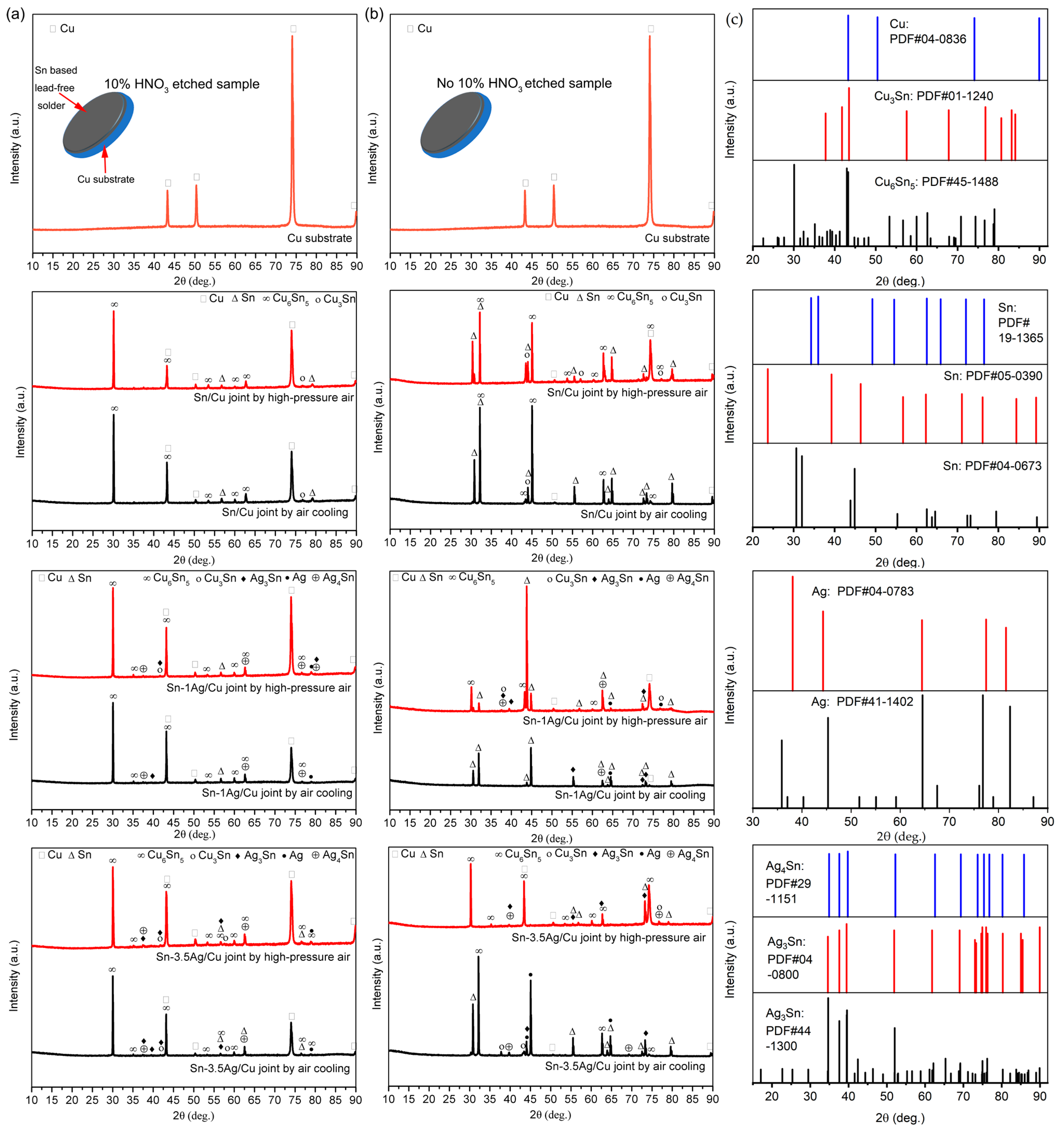
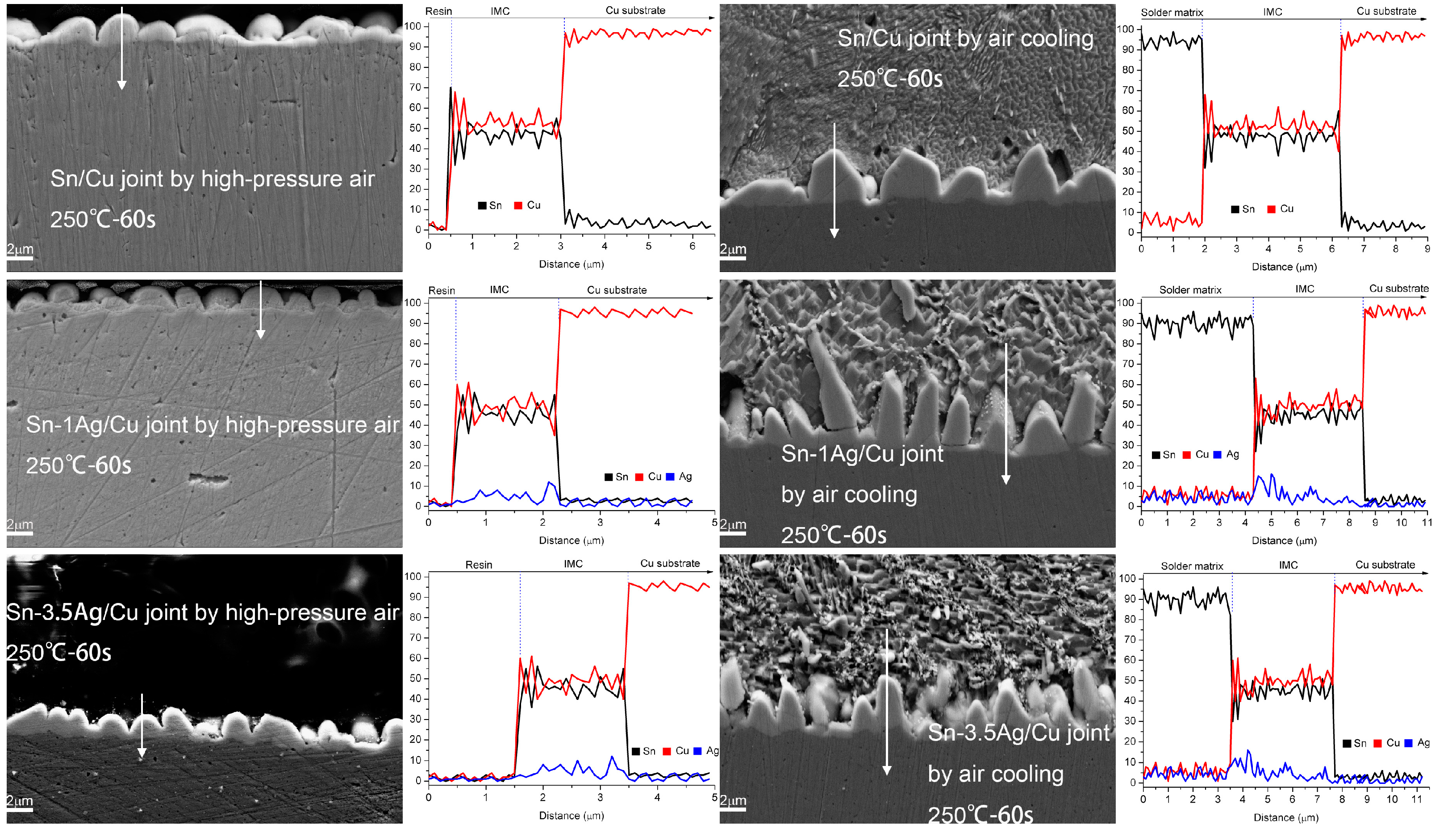
3.1. Analysis of Intermetallic Phases and Its Composition Soldering Joint Interface

When the Ag element is present in the solder, it will affect the growth of Cu6Sn5 at the interface. Figure 2 shows the Sn-Ag binary phase diagram. From the figure, it can be seen that when the Ag content is more than (including 3.5 wt.%) 3.5 wt.%, there are unstable Ag3Sn cluster structures in the liquid Sn solder [17]. But for the Ag content is less than 3.5 wt.%, the Ag element exists as atoms in the solder. When the soldering temperature decreases (the cooling stage), the Sn-Ag solder will precipitate a stable Ag3Sn phase. From the above description, it can be seen that for Sn-3.5Ag solder, the form, and size of Ag3Sn exist differently during the heat preservation and cooling stages, and the influence mechanism on the growth of Cu6Sn5 grain at the interface is also different. Due to the instability of the Ag3Sn phase formed during the heat preservation stage and its continuous dynamic changes only in the form of short-range clusters (Ag3Sn was a small amount of phase and most of Ag element still exists as Ag atoms, which is consistent with Qu’s discovery that the Ag3Sn phase during the early cooling stage was very small, few, and unstable [3]) as shown in the following formula: A g 3 S n T 3 A g + S n . However, for Sn-1Ag solder, the Ag element exists as Ag atoms in the solder to influent the growth of Cu6Sn5 grain until the cooling stage begins.
The identity of the intermetallic phases was also experimentally verified by an XRD pattern, as shown in Figure 3. From the XRD diagram, it can be seen that there are a total of four phases, such as Cu, Sn, Cu6Sn5, and Cu3Sn phase, for Sn/Cu soldering joints. But for Sn-Ag/Cu joints, in addition to the four phases described above, the other three phases (Ag, Ag3Sn, Ag4Sn) have also been detected. The EDX line-scan for Cu and Sn-base solder across the interface (The direction and position of line scanning are shown by the arrows in the figure) were also prove that there are two elements, Sn and Cu, at the Sn/Cu interface, while Sn-Ag/Cu interface has three elements (Sn, Ag, and Cu) in Figure 4. The Ag peak of the XRD pattern (Figure 3) also directly proves the existence of Ag particles (namely, Ag atom [18,19]). The presence of Ag nanoparticles will facilitate the formation of Cu-Sn bonds, leading to a faster increase in the thickness of the Cu6Sn5 layer at the Sn-Ag/Cu soldering interface than that at Sn/Cu, as shown in Figure 5h,j and Figure 6c. From the XRD spectrum, it was also found that the Ag phase often coexists with the Ag3Sn phase and Ag4Sn phase at the same detection peak. It is also difficult for us to distinguish the location of the Ag phase and the stage of the soldering process. The preliminary research results of the author and his research team also indicate that the Ag3Sn phase [2], but not the Ag phase (not observed), is stable during the cooling stage, while the Ag3Sn phase is in a dynamic process of continuous dissolution and formation during the heat preservation stage [3]. It can be simply inferred that the Ag phase basically exists during the heat preservation stage of soldering. As we all know from the Sn-Ag binary phase diagram (Figure 2) [17,20,21,22], when the soldering temperature decreases, the activity of the Ag phase and its saturation and diffusion properties in the molten Sn medium continue to decrease, leading to the continuous precipitation of Ag atoms to form metastable (Ag4Sn [18]) or stable (Ag3Sn [2,23]) Ag containing compounds. In the cooling stage, the cooling rate of the solder joint is first fast and then slow, resulting in a high degree of undercooling in the early stage [2]. In the case of high Ag concentration and high undercooling, this is conducive to the formation of the Ag4Sn phase (the nucleation-free energy of the Ag4Sn phase is greater than that of Ag3Sn [19]). As mentioned in reference [18], at the initial stage of cooling, supersaturation Ag atoms and liquid Sn first form the Ag4Sn phase through peritectic reaction: A g h i g h   c o n c e n t r a t i o n + S n ( l o w   c o n c e n t r a t i o n ) A g 4 S n . As the temperature further decreases, the Ag4Sn phase undergoes a eutectic reaction with the remaining liquid phase Sn to form the Ag3Sn phase: A g 4 S n + S n ( L ) A g 3 S n . Therefore, at the end of the equilibrium soldering process, there is a eutectic structure (the remaining liquid Sn phase and Ag3Sn phase), and there may also be a mixed non-equilibrium structure of Ag3Sn wrapped in the outer layer of the incompletely transformed Ag4Sn.
Finally, the presence of Ag element at the Sn-Ag/Cu interface was also found through EDX line scanning, which indirectly proves that Ag atoms are active and exist in the heat preservation stage of soldering. However, during the cooling stage, they exist in the form of some equilibrium (Ag@Ag3Sn) or nonequilibrium compound (Ag@Ag4Sn).

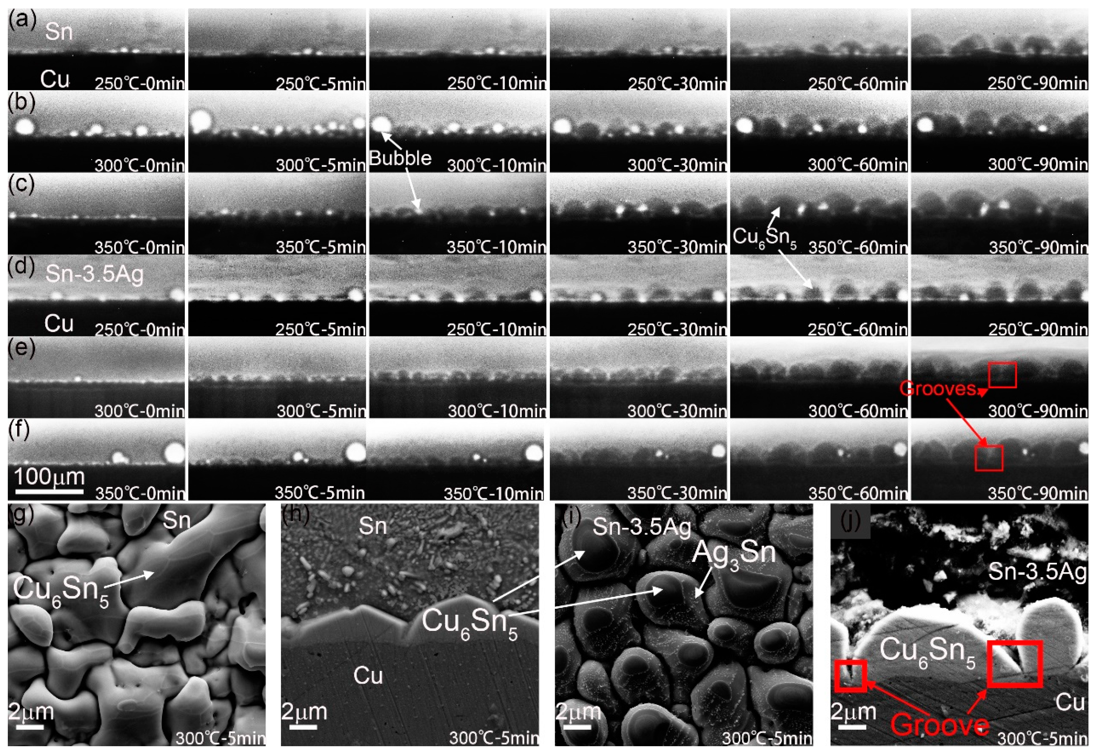
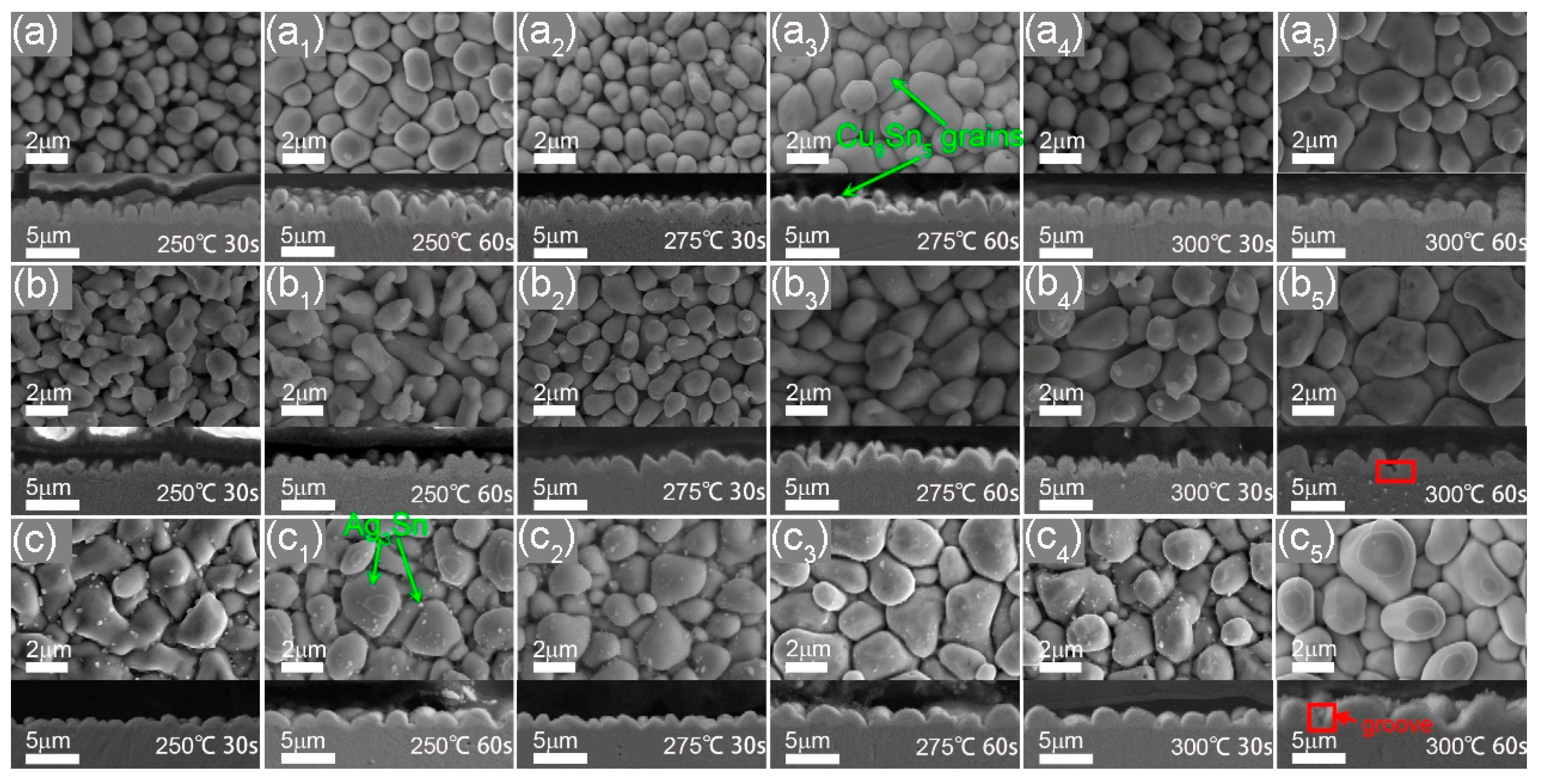
3.2. Microstructure of Interface IMC during the Heat Preservation Stage

The in-situ observation results of the heat preservation stage of the reflow soldering experiment, as characterized by the synchrotron radiation-based X-ray images, are presented in Figure 5a–f, whereas the ex-situ results characterized by SEM images are shown in Figure 5g–j. In the X-ray images a–f, the Cu substrate appears as the black region, the liquid solder is seen as gray-colored, and the Cu6Sn5 IMCs appear in the intermediate color between solder and substrate. The white-colored portions at the interface are the gaseous bubbles, which are caused by the inability to exhaust gas in a timely manner during soldering melting. Due to the randomness of bubbles, different sizes and quantities of bubbles may appear in different soldering joints. Therefore, it is necessary to eliminate the influence of bubbles on the growth of Cu6Sn5 at the interface as much as possible, but not significant for the grooves formed between adjacent grains (not affecting the movement of Ag atoms).
In the context of the synchrotron radiation results in Figure 5a–c for IMC formed due to L-S interfacial reaction in Sn/Cu system, it can be observed that the size of the scalloped compound is considerably larger at the later stages of the soldering reflow time. Moreover, the experimental IMC sizes corresponding to a given time point are larger in the context of higher temperature reflow experiments. The experimental results in Sn-3.5Ag/Cu joints, as in Figure 5d–f, show the same trend of size in relation to reaction time and reflow temperature. However, the grain morphology of IMC at the interface of Sn-3.5Ag/Cu appears different than that of the Sn/Cu system, and the distinction between them can be observed more clearly at the latter stages of in situ reactions. At t = 90 min or 1.5 h, it can be inferred that the scalloped IMCs of the Sn/Cu system do not have observable furrow between them, whereas IMCs at the interface of Sn-3.5Ag/Cu are characterized by the presence of narrow mechanical grooves [10] or channel between them. The in situ observation of furrow formations in Sn-Ag solders is supported by the cross-section SEM results as in Figure 5i,j, in which grooves are present only in the case of IMC corresponding to the Sn-Ag/Cu system. Notably, in the isothermal reflow heating experiment characterized by a small magnitude of Jackson’s parameter (αJ < 2) [24], the top view of IMC for both the solder types in Figure 5g,h are evidently scalloped, and additionally, the Sn-Ag solder related IMC is characterized by the presence of nano-sized Ag3Sn particles. Notably, the Ag3Sn nanoparticles distribution is denser at the peripheral surface of the Cu6Sn5 grains. This distribution pattern is more likely to shield and inhibit the lateral growth of Cu6Sn5 grains on the one hand, whereas it alters the grain boundary diffusion mechanism on the other hand.
Figure 5. The real-time results for isothermal reflow heating in liquid Sn/solid Cu system at different constant temperature are shown in figures (ac). The corresponding results for Sn-3.5Ag/Cu system are presented in figures (df). The pictures (g,i) represent top and cross-section views respectively obtained under SEM for interfacial IMC of Sn/Cu undergoing liquid removal via air jet. The corresponding images for SEM results in Sn-Ag/Cu systems are shown in figures (h,j).
Metals 13 01445 g005
The measurements related to interfacial IMC for the in situ experiments with Sn and Sn-3.5Ag solders were obtained in accordance with the methodology utilized in the work of Qu et al. [25]. With the help of real-time imaging technique, the experimental data of the number of IMC scallops per interface length as well as average height (h), width (w), and aspect ratio (w/h) of individual IMC grains for each solder sample type have been plotted against time for several temperatures in Figure 6a–d. From the figure, it can be seen that with the extension of soldering temperature and time, the number of IMC grains continues to decrease while the IMC grain width, IMC layer thickness, and IMC grain aspect ratio all continue to increase. Under the same reflux conditions, compared to the Sn/Cu interface, the Sn-3.5Ag/Cu interface has more IMC grains, smaller grain width and aspect ratio, and larger IMC layer thickness. This indicates that the addition of Ag element inhibits the lateral annexation and growth of Cu6Sn5 grains, promotes the longitudinal growth, and leads to a smaller aspect ratio of Cu6Sn5 grains at the Sn-3.5Ag/Cu interface and a larger IMC layer thickness.
At a given temperature, the number of IMC grains per unit interface length is greater for Sn-3.5Ag solders in accordance with Figure 6a, thus implying the Cu6Sn5 grains are wider in the context of pure Sn solder, as depicted in Figure 6b. In general, both the w and h of an IMC grain for the Sn/Cu and Sn-Ag/Cu systems increase with the experimental time and temperature. But considering the aspect ratio data for samples in Figure 6d, it is obvious that the lowest aspect ratio for Sn/Cu at an experimental temperature value of 350 °C stands on top of the greatest aspect ratio for Sn-3.5Ag/Cu at 250 °C. The w or numerator term in an aspect ratio of pure Sn solder sample increasing at a faster rate than that for Sn-Ag solder and denominator h of pure Sn specimens increasing at a slower rate than the Sn-3.5Ag specimens will have a double effect in the higher magnitude of an aspect ratio of Sn/Cu solders as compared to Sn-3.5Ag/Cu solders. From this, it can be inferred that the height of Sn-3.5Ag solders is increased at a faster rate than that of pure Sn solders, whereas the increment in width of the former is somehow constrained by the formation of channels. Moreover, as shown by Figure 6c, it is verified that the height of IMC for the Sn-3.5Ag/Cu system at a given temperature is greater than that for Sn/Cu joints, and this difference is more pronounced at the latter stages of interfacial reaction maintained at a constant temperature. For example, at 350 °C and at t = 1.5 h, the magnitude of h attained by IMC for Sn-Ag solder is 22 μm, whereas that for pure Sn is just only 20 μm. The Cu6Sn5 IMC for Sn solder at 250 °C attains a height of 12 μm by the end of 1.5 h, and the IMC for Sn-Ag solders at the same time period of time exceeds it with a difference of less than 1 μm.
Figure 6. (a) shows the plot of time versus average number of IMC scallops per 665 μm (=2048 pixels × 0.325 μm/pixels) of interface length for the Sn/Cu and Sn-Ag/Cu systems at the temperatures 250, 300 and 350 °C. The figures (b) and (c), respectively, correspond to the average width (w) and height or thickness (h) of an IMC grain, whereas the picture in (d) illustrates the variation of aspect ratio (w/h) of a grain with time for the solder systems. All the measurements have been obtained from the in-situ experimental results.
Metals 13 01445 g006
Due to the low resolution of synchrotron radiation, the definition of Synchrotron radiation pictures is low. Therefore, we used high-resolution SEM to study the effect of different Ag concentrations on the interface IMC growth during the heat preservation stage. Figure 7 is SEM images of the top-view and cross-sectional morphologies of IMC formed at Sn-XAg/Cu interfaces (X = 0, 1, 3.5) under 250/275/300 °C with 30 s and 60 s during the heat preservation stage. From Figure 7, we can see that the IMC grains are all scalloped in shape with various soldering conditions. With the soldering time and temperature increasing, the grains grow bigger. For Sn and Sn-1Ag solders, the morphology of IMC is very similar to each other. But, for Sn-3.5Ag solder, the morphology of IMC is higher, and the IMC thickness is also thicker. In addition, nano Ag3Sn particles appear on the boundary surface of existing Cu6Sn5 grains at Sn-3.5Ag/Cu interface, not at Sn-1Ag/Cu interface. That is because the high-pressure air may not be clear enough to remove the liquid solder matrix, especially high Ag solder Sn-3.5Ag. So, we can see some nano Ag3Sn particles appear on the existing Cu6Sn5 grains. Meantime, the Ag concentration is smaller in Sn-1Ag solder than that in Sn-3.5Ag solder so that the Ag3Sn is easier to appear at the Sn-3.5Ag/Cu interface by high-pressure air. Obviously, it can be seen that the groove appears at the interface of Ag-containing solder/Cu soldering joints, as shown in Figure 7, which get a similar result with synchrotron radiation.

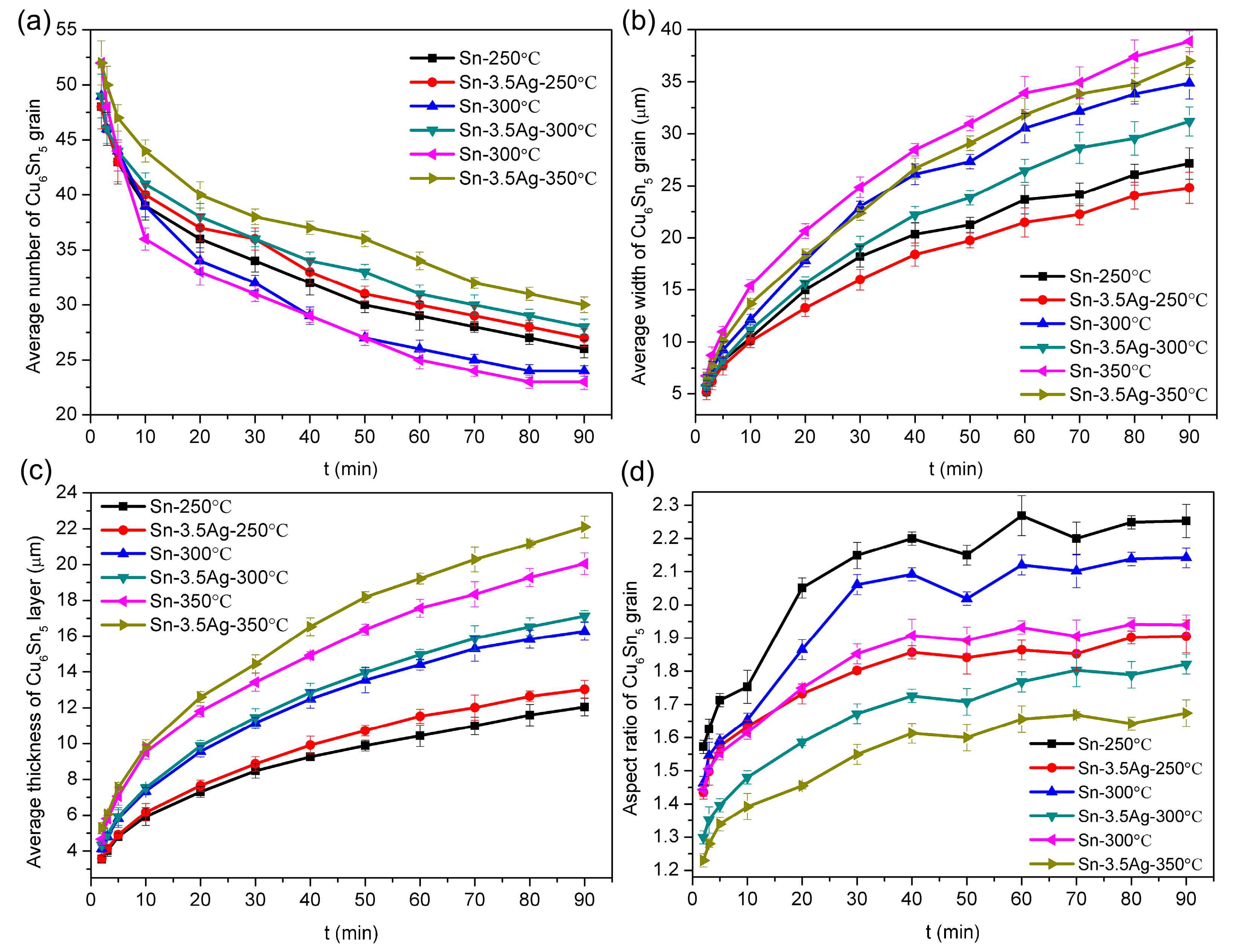
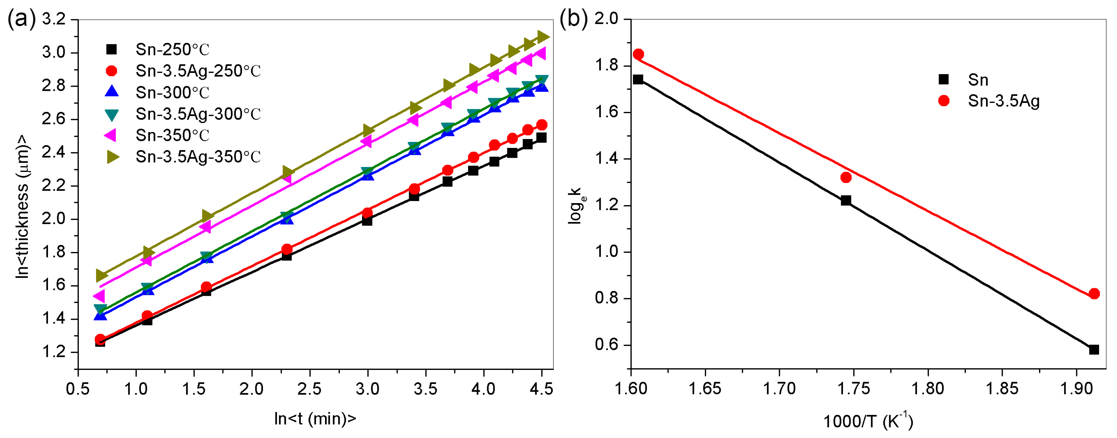
3.3. Growth Dynamics Analysis of Interface IMC during the Heat Preservation Stage

From the viewpoint of reliability, the growth kinetics of IMC height (h) has been considered significant. The thickness increase of intermetallic compound during L-S interfacial reaction in solder/substrate pair at an isothermal temperature T is given as [17]:
h ( t , T ) = k × t n
k = k 0 exp ( Q R T )
In Equations (2) and (3), k is the growth rate coefficient, k0 is constant, t is the reaction time, and n is the kinetic exponent, Q is the activation energy of Cu6Sn5 growth, R is the Boltzman constant (8.314 kJ/mol), and T is soldering isothermal temperature. In logarithmic form, Equations (2) and (3) can be rewritten as
ln h = Q R T + n ln t
Figure 8 is the linear fitting curve of thickness and activation energy of Cu6Sn5 growth at the Sn/Cu and Sn-3.5Ag/Cu systems for soldering time 90min. The growth index (n), growth rate coefficient (k), and growth activation energy (Q) calculated using Formulas (3) and (4) are listed in Table 1.
From Figure 8a and Table 1, the measured values of n show approximately t1/3 dependence on time, and thus, the IMC formation via interfacial reactions for both Sn and Sn-Ag solders type is mainly dominated by the grain boundary diffusion [26]. The growth rate constant k for both the solders increases with T, and notably, the growth rate constant for Sn-3.5Ag/Cu at a given temperature is greater than the corresponding value for Sn/Cu joints. At 250 °C, there is only a slight difference of 0.0044 μm/min−1/3 in the magnitudes of k between Sn-3.5Ag and Sn solders, whereas the differences account for 0.0996 and 0.3896μm/min−1/3 at temperatures of 300/350 °C, respectively. Despite the fact that Ag3Sn particle shield or suppress the lateral growth of Cu6Sn5 [9], the presence of these particles is associated with enhanced height or thickness of Cu6Sn5 grain in isothermal L-S conditions. This vertical growth but lateral suppression of IMC growth can occur only if there is an enhanced rate of Cu supply from the substrate. As we know from the analysis in Section 3.1, the Ag element exists as Ag atoms in the low silver solder to influent the growth of Cu6Sn5 grain until the cooling stage begins. There may be the possibility of a grooving effect caused due to the presence of Ag nanoparticles at the interface of the solder/substrate system, which then can establish routes for promoting the grain-boundary diffusion-controlled growth of Cu6Sn5 in the L-S interface of Sn-3.5Ag/Cu solder [15] and this effect is more pronounced at higher temperatures. Based on the above analysis, it can be concluded that during the insulation stage, the addition of the Ag element reduces the activation energy of Cu6Sn5 growth at the interface (Table 1), and the obtained growth activation energy is within the range of activation energy obtained of the soldering process by other scholars (27 KJ·mol−1~64.8 KJ·mol−1) [16]. Compared with the low-temperature aging process, the diffusion ability of atoms in the brazing stage is much greater than that in the aging process. Therefore, it can be seen that the atomic nucleation energy and compound growth activation energy in the molten state are much lower than those in the solid-state aging process [2,3,4,5,9,10,15,16,17,24]. Ag nanoparticles and Ag3Sn clusters (unstable and very few) only exist in the solder, adsorbing in the high-energy region of the grain boundary, hindering the lateral annexation and migration of the grain boundary to retain the grooves between the adjacent grains, thereby promoting the growth of Cu6Sn5 at the interface. Therefore, the addition of the Ag element leads to a decrease in the activation energy of Cu6Sn5 growth, promoting the continuous thickening of the Cu6Sn5 layer.

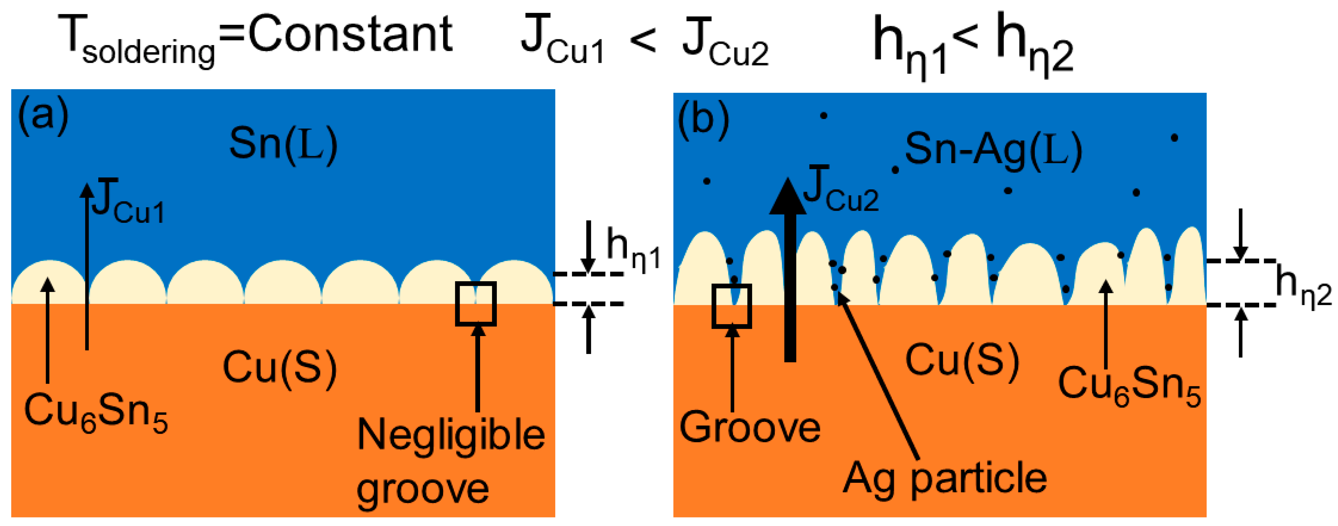
3.4. Grooving Effect of Ag Particles on the Growth Mechanism of Interface IMC

Figure 9 represents the schematic diagram to explain the mechanism of alteration of grain boundary diffusion of Cu into the molten solder in the presence of a third particle, namely Ag, at the interface (blue represents Sn based solder, yellow represents intermetallic compound (Cu6Sn5), and reddish brown represents polycrystalline Cu substrate). During the interfacial reaction of Sn and Cu and assuming grain boundary diffusion is more dominant than the bulk diffusion, the flux of Cu into the Sn or Sn-3.5Ag solder is given by the following expression [27,28]:
J C u , g b = D C u × S g b × ρ l C b C e w
wherein DCu is the diffusivity of Cu in liquid solder, w is the grain width, and ρl is the density of solder. Ce and Cb are the equilibrium concentrations of Cu at solder/Cu6Sn5 interface and Cu6Sn5/Cu grain boundary interfaces, respectively. Sgb is the area proportion of the grain boundary channel to the total grain area and is expressed as
S g b = 1 1 + 3 w 2 δ
The channel width of the grain boundary [26,27], δ is represented as lgb for Sn, and l*gb for Sn-3.5Ag solders in Figure 9. From Equations (5) and (6), it can be inferred that the diffusion flux of Cu increases when δ is large and w is smaller. In the presence of Ag particles of radius r at the grain boundary of Cu, the zener pinning effect, by inducing thermal grooving [29], will constrain the growth of Cu grains [30] and thus reduce the grain width (w). Moreover, the pinning of Ag on the Cu grain boundary will induce the latter to attain a catenoid-like shape in 3D after being subjected to particle pressure (P), whose maximum value is given as [31]:
P max = 3 2 × γ g b r × f v
wherein γgb is the surface energy at the grain boundary and fv is the volume fraction of the Ag nanoparticles along the grain boundaries. The result of this pinning effect in different orientations will induce a thermal grooving effect at the grain boundaries. This will lead to the selective-orientation growth of Cu6Sn5 within shrinking grains of basal polycrystalline Cu, and the subsequent result is the enlargement of nano-grain boundary channels at the interface of Sn-3.5Ag/Cu solders. Thus, with greater width (l*gb) of grain boundary channel and smaller basal grain size of IMC (w*3 in Figure 9), the flux of Cu into the solder is enhanced in accordance with Equation (3), and thus, the final Cu6Sn5 will attain a greater height (h*3 in Figure 9) in context of Sn-3.5Ag/Cu solder joints. This explanation is supported by the experimental results presented in Figure 5. wherein the IMC of pure Sn solders are observed to have larger basal grain width, lower number of scallops per interface length, and smaller height as compared to the IMC of Sn-3.5Ag solders. The pinned Ag at the Cu grain boundaries will subsequently react with liquid solder to form Ag3Sn nano-particles which are mostly found to concentrate along the grain boundary [32], as evidenced in Figure 5j. The incremental difference of height attainment by IMCs of Sn-Ag and Sn solders as the temperature is elevated can be explained by the dependence of the pinning effect on the surface energy of grain boundary (Equation (7)).
From the perspective of diffusion flux, Figure 10 is the schematic diagram of the effects of the Ag3Sn cluster on the flux of Cu of interfacial IMC growth at the heat preservation stage of Sn/Cu and Sn-3.5Ag/Cu soldering interfaces (blue represents Sn based solder, yellow represents intermetallic compound (Cu6Sn5), and reddish brown represents polycrystalline Cu substrate). In the interface reaction process between Sn and Cu, grain boundary diffusion is more dominant than bulk diffusion [33]. The flux of Cu atoms entering Sn or Sn-3.5Ag solder through grain boundaries, JCu, can be expressed using Formula (5) [28].
From the phase diagrams of Sn-Cu and Sn-Ag [17,34,35], it can be seen that the equilibrium concentration of Cu at the interface between Sn solder and Cu6Sn5 is slightly higher than that in Sn-Ag solder. From Figure 9, it can be seen that the total width of grain boundary gaps at the Sn-Ag/Cu interface is greater than that at the Sn/Cu interface. Therefore, more Cu atoms can reach the Cu6Sn5/Cu grain boundary interface, where the equilibrium concentration (CCu) of the Cu6Sn5/grain boundary (GB) interface in Sn-Ag solder is greater than that in Sn solder. Therefore, compared to the Sn/Cu interface, the values of (CCu) and Sgb are larger at the Sn-Ag/Cu interface. According to Formulas (4) and (5), the diffusion flux JCu2 at the grain boundary of the Sn-Ag/Cu interface is relatively higher.
The distribution results of Cu concentration in Sn-xAg solder are basically the same, so the Cu flux flowing into the solder body from the interface reaction zone is the same [2]. Based on the above analysis, it can be concluded that the Cu flux of IMC grown at the Sn-Ag interface IMC is greater than that that at the Sn/Cu interface. Therefore, during the heat preservation stage, the IMC thickness of the Sn-Ag/Cu interface is relatively thicker than that of the Sn/Cu interface.
From the above analysis, it can be seen that during the heat preservation stage, the addition of the Ag element not only changes the micromorphology of interface IMC but also changes the Cu concentration in different regions of the solder body to inhibit the dissolution of interface IMC and promote the growth of interface IMC. This article can explain the mechanism of the influence of Ag particles on the Sn-Ag/Cu soldering interface. However, the observation of Ag nanoparticles during the heat preservation and cooling stages still needs to be continued so as to better explain the interface reaction mechanism during the heat preservation stage. At present, the mechanism of the influence of Ag and Ag3Sn particles on the liquid–solid interface reaction during the heat preservation and cooling stages of soldering has been studied. Subsequent research will continue to investigate the influence mechanism of two types of particles on the solid–solid interface reaction during service time, as well as their lifespan under different service conditions (such as thermal cycling, thermoelectric coupling, salt spray corrosion).

4. Conclusions

In summary, it has been demonstrated through in situ synchrotron radiation-based experiments that Sn-Ag solders are characterized by mechanically grooved interfacial IMC, and this effect can be correlated with the enhancement of Cu grain boundary diffusion into liquid solder and subsequent formation of IMC with larger heights during isothermal reflow soldering. Moreover, the thermal grooving effect in the Cu substrate is associated with the formation of smaller widths and selectively oriented Cu6Sn5 IMC in the Sn-3.5Ag solders.

Author Contributions

Design and idea of the paper, H.M.; resources, H.M.; data curation, B.G.; writing—original draft preparation, B.G.; writing—review and editing, B.G. and A.K.; image drawing and date processing, B.G. and A.K.; preparation of soldering samples, R.W.; metallographic treatment and characterization of soldering samples, H.Z.; funding acquisition, H.M. All authors have read and agreed to the published version of the manuscript.

Funding

This work was supported by the Youth Natural Science Foundation Project of Jiangxi Provincial Department of Science and Technology (Grant Nos. 20224BAB214012), Student Innovation and Entrepreneurship Training Program of Yichun University (Grant Nos. 202010417079 and S202310417007) and Yichun University’s 2021 Education Reform Project (Grant Nos: 209/P320152221).

Data Availability Statement

The data presented in this study are available in the article.

Acknowledgments

The authors acknowledge the support by the synchrotron radiation experiments were performed at the BL13W1 beamline of Shanghai Synchrotron Radiation Facility (SSRF), China.

Conflicts of Interest

The authors declare no conflict of interest.

References

  1. Kim, G.; Son, K.; Lee, J.H.; Joo, Y.C.; Park, Y.B. Size effect on the electromigration characteristics of flip chip pb-free solder bumps. Electron. Mater. Lett. 2022, 18, 431–439. [Google Scholar] [CrossRef]
  2. Guo, B.F.; Kunwar, A.; Zhao, N.; Chen, J.; Wang, Y.P.; Ma, H.T. Effect of Ag3Sn nanoparticles and temperature on Cu6Sn5 IMC growth in Sn-xAg/Cu solder joints. Mater. Res. Bull. 2018, 99, 239–248. [Google Scholar] [CrossRef]
  3. Ma, H.T.; Qu, L.; Huang, M.L.; Zhao, N.; Wang, L. In-Situ study on growth behavior of Ag3Sn in Sn-3.5Ag/Cu soldering reaction by synchrotron radiation real-time imaging technology. J. Alloys Compd. 2012, 537, 286–290. [Google Scholar] [CrossRef]
  4. Ma, H.R.; Kunwar, A.; Guo, B.F.; Sun, J.H.; Jiang, C.R.; Wang, Y.P.; Song, X.G.; Zhao, N.; Ma, H.T. Effect of cooling condition and Ag on the growth of intermetallic compounds in Sn-based solder joints. Appl. Phys. A Mater. Sci. Process. 2016, 122, 1052. [Google Scholar] [CrossRef]
  5. Kunwar, A.; Ma, H.R.; Ma, H.T.; Sun, J.H.; Zhao, N.; Huang, M.L. On the increase of intermetallic compound’s thickness at the cold side in liquid Sn and SnAg solders under thermal gradient. Mater. Lett. 2016, 172, 211–215. [Google Scholar] [CrossRef]
  6. Cabrales, H.D.N.; Arroyo, L.O.; Silva, I.C.; Caballero, I.M.; Pardavé, M.P.; González, J.A.; Borja, R.P.P. Influence of TiO2 nanoparticles content as reinforce material to enhance the mechanical and corrosion resistance properties of Sn and Sn-Ag alloy for dental applications. J. Mech. Behav. Biomed. 2023, 140, 105687. [Google Scholar] [CrossRef]
  7. Yakymovych, A.; Shtablavyi, I. Effect of nanosized Ni reinforcements on the structure of the Sn-3.0Ag-0.5Cu alloy in liquid and after-reflow solid states. Metals 2023, 13, 1093. [Google Scholar] [CrossRef]
  8. Yeh, C.Y.; Wang, J.Y.; Wu, C.Y.; Chiu, C.Y.; Lee, C.H.; Huang, B.R.; Fu, K.L.; Chang, J.S.; Yen, T.H.; Lee, Y.F.; et al. Development of growth model on interfacial intermetallic compound at circular Cu/Sn3.5Ag interface. J. Mater. Sci. Mater. Electron. 2022, 33, 25580–25588. [Google Scholar] [CrossRef]
  9. Yang, M.; Ji, H.J.; Wang, S.; Ko, Y.H.; Lee, C.W.; Wu, J.X.; Li, M.Y. Effects of Ag content on the interfacial reactions between liquid Sn-Ag-Cu solders and Cu substrates during soldering. J. Alloys Compd. 2016, 679, 18–25. [Google Scholar] [CrossRef]
  10. Yang, M.; Li, M.Y.; Wang, C.Q. Interfacial reactions of eutectic Sn3.5Ag and pure tin solders with Cu substrates during liquid-state soldering. Intermetallics 2012, 25, 86–94. [Google Scholar] [CrossRef]
  11. Sobral, B.S.; Vieira, P.S.; Lima, T.S.; Spinelli, J.E.; Cheung, N.; Garcia, A.; Silva, B.L. Effects of Zn addition on dendritic/cellular growth, phase formation, and hardness of a Sn–3.5 wt% Ag solder alloy. Adv. Eng. Mater. 2023, 25, 2201270. [Google Scholar] [CrossRef]
  12. Barik, E.M.; Gillot, C.; Hodaj, F. Bubble formation and growth during Transient Liquid Phase Bonding in Cu/SnAg system for microelectronic packaging. J. Mater. Sci. Mater. Electron. 2022, 33, 2360–2374. [Google Scholar] [CrossRef]
  13. Wang, X.; Zhang, L.; Li, M.L. Microstructure and properties of Sn-Ag and Sn-Sb lead-free solders in electronics packaging: A review. J. Mater. Sci. Mater. Electron. 2022, 33, 2259–2292. [Google Scholar] [CrossRef]
  14. Guo, B.F.; Ma, H.T.; Kunwar, A.; Chu, X.H. Effect of the degree of supercooling on growth mechanism of Cu6Sn5 in pure Sn/Cu solder joint. J. Mater. Sci. Mater. Electron. 2021, 32, 7528–7540. [Google Scholar] [CrossRef]
  15. Ma, H.T.; Kunwar, A.; Sun, J.H.; Guo, B.F.; Ma, H.R. In Situ study on the increase of intermetallic compound thickness at anode of molten tin due to electromigration of copper. Scr. Mater. 2015, 107, 88–91. [Google Scholar] [CrossRef]
  16. Guo, B.F.; Kunwar, A.; Jiang, C.R.; Zhao, N.; Sun, J.H.; Chen, J.; Wang, Y.P.; Huang, M.L.; Ma, H.T. Synchrotron radiation imaging study on the rapid IMC growth of Sn-xAg solders with Cu and Ni substrates during the heat preservation stage. J. Mater. Sci. Mater. Electron. 2017, 33, 36–72. [Google Scholar] [CrossRef]
  17. Li, J.F.; Agyakwa, P.A.; Johnson, C.M. Kinetics of Ag3Sn growth in Ag-Sn-Ag system during transient liquid phase soldering process. Acta Mater. 2010, 58, 3429–3443. [Google Scholar] [CrossRef]
  18. Dai, W.; Liu, Y.Y.; Huang, N.G.; Lan, R.L.; Zheng, K.K.; Lu, Y.X.; Li, J.; Jiang, Y.M.; Sun, Y.T. Selective corrosion of β-Sn and intermetallic compounds in an Ag–Sn alloy at different potentials in NaCl and Na2SO4 solutions. Corros. Sci. 2023, 212, 110958. [Google Scholar] [CrossRef]
  19. Schmuelling, G.; Oehl, N.; Fromma, O.; Knipper, M.; Olesiak, J.K.; Plaggenborg, T.; Parisi, J.; Winter, M.; Placke, T. Synthesis and electrochemical characterization of nano-sized Ag4Sn particles as anode material for lithium-ion batteries. Electrochim. Acta 2016, 196, 597–602. [Google Scholar] [CrossRef]
  20. Manasijevi, D.; Balanovi, L.; Markovi, I.; Gorgievski, M.; Stamenkovíc, U.; Đorđevíc, A.; Miníc, D.; Cosovi, V. Structural and thermal properties of Sn-Ag alloys. Solid State Sci. 2021, 119, 106685. [Google Scholar] [CrossRef]
  21. Shalaby, R.M. Development of holmium doped eutectic Sn-Ag lead-free solder for electronic packaging. Solder. Surf. Mt. Technol. 2022, 34, 277–286. [Google Scholar] [CrossRef]
  22. Hou, N.; Xian, J.W.; Sugiyama, A.; Yasuda, H.; Gourlay, C.M. Ag3Sn morphology transitions during eutectic growth in Sn–Ag alloys. Metall. Mater. Trans. A 2023, 54 Pt A, 909–927. [Google Scholar] [CrossRef]
  23. Cui, Y.; Xian, J.W.; Zois, A.; Marquardt, K.; Yasuda, H.; Gourlay, C.M. Nucleation and growth of Ag3Sn in Sn-Ag and Sn-Ag-Cu solder alloys. Acta Mater. 2023, 249, 118831. [Google Scholar] [CrossRef]
  24. Choi, W.K.; Jang, S.Y.; Kim, J.H.; Paik, K.W.; Lee, H.M. Grain morphology of intermetallic compounds at solder joints. J. Mater. Res. 2002, 17, 597–599. [Google Scholar] [CrossRef] [Green Version]
  25. Qu, L.; Zhao, N.; Zhao, H.J.; Huang, M.L.; Ma, H.T. In situ study of the real-time growth behavior of Cu6Sn5 at the Sn/Cu interface during the soldering reaction. Scr. Mater. 2014, 72–73, 43–46. [Google Scholar] [CrossRef]
  26. Schaefer, M.; Fournelle, R.A.; Liang, J. Theory for intermetallic phase growth between cu and liquid Sn-Pb solder based on grain boundary diffusion control. J. Electron. Mater. 1998, 27, 1167–1176. [Google Scholar] [CrossRef]
  27. Kim, H.K.; Tu, K.N. Kinetic analysis of the soldering reaction between eutectic SnPb alloy and Cu accompanied by ripening. Phys. Rev. B 1996, 53, 16027–16034. [Google Scholar] [CrossRef] [PubMed]
  28. Huang, M.L.; Yang, F. Size effect model on kinetics of interfacial reaction between Sn-xAg-yCu solders and Cu substrate. Sci. Rep. 2014, 4, 7117. [Google Scholar] [CrossRef] [PubMed] [Green Version]
  29. Hummel, R.E.; Goho, S.M.; DeHoff, R.T. The role of thermal grooving, thermotransport and electrotransport on the failure of thin film metallizations. In Proceedings of the 22nd International Reliability Physics Symposium, Las Vegas, NV, USA, 3–5 April 1984; pp. 234–241. [Google Scholar]
  30. Moelans, N.; Blanpain, B.; Wollants, P. Pinning effect of second-phase particles on grain growth in polycrystalline films studied by 3-D phase field simulations. Acta Mater. 2007, 55, 2173–2182. [Google Scholar] [CrossRef]
  31. Tonks, M.R.; Zhang, Y.; Butterfield, A.; Bai, X.M. Development of a grain boundary pinning model that considers particle size distribution using the phase field method. Model. Simul. Mat. Sci. Eng. 2015, 23, 045009. [Google Scholar] [CrossRef]
  32. Sharps, P.R.; Tomsia, A.P.; Pask, J.A. Wetting and spreading in the Cu-Ag system. Acta Metall. 1981, 29, 855–865. [Google Scholar] [CrossRef] [Green Version]
  33. Sun, J.; Zhao, L.Y.; Liang, H.X.; Zhang, Y.; Li, X.X.; Teng, C.Y.; Wang, H.; Bai, H.L. A review on phase field modeling for formation of η-Cu6Sn5 intermetallic. Metals 2022, 12, 2043. [Google Scholar] [CrossRef]
  34. Moon, K.W.; Boettinger, W.J.; Kattner, U.R.; Biancaniello, F.S.; Handwerker, C.A. Experimental and thermodynamic assessment of Sn-Ag-Cu solder alloys. J. Electron. Mater. 2000, 29, 1122–1136. [Google Scholar] [CrossRef]
  35. Hamasha, M.M.; Hamasha, K.; Hamasha, S. Impact of isothermal aging on mechanical properties of 92.8%Sn-3%Ag-0.5%Cu-3.3%Bi (cyclomax) solder joints. Metals 2023, 13, 591. [Google Scholar] [CrossRef]
Figure 1. A schematic diagram to illustrate the experimental setup for (a) in situ observation of isothermal reflow soldering in Sn/Cu and Sn-3.5Ag/Cu systems at SSRF, (b) high-pressure air gun system for ex situ characterization of isothermal reflow results.
Metals 13 01445 g001
Figure 2. Sn-Ag binary phase diagram.
Metals 13 01445 g002
Figure 3. XRD analysis results of Sn-based lead-free solder/Cu soldering joints: (a) 10% HNO3 etched samples; (b) No 10% HNO3 etched samples; (c) PDF card of physical phase.
Metals 13 01445 g003
Figure 4. Microstructures and EDX line-scan images of Sn-base solder/Cu soldering joints.
Metals 13 01445 g004
Figure 7. SEM images of the top-view and cross-sectional morphologies of the IMC grains at (aa5) Sn/Cu, (bb5) Sn1Ag/Cu, and (cc5) Sn-3.5Ag/Cu interfaces with soldering time of 30 s and 60 s at 250/275/300 °C by high-pressure air.
Metals 13 01445 g007
Figure 8. (a) Linear fitting curve of thickness and (b) activation energy of Cu6Sn5 growth at the Sn/Cu and Sn-3.5Ag/Cu systems.
Metals 13 01445 g008
Figure 9. The schematic sketch shows the absence and presence of thermal grooving mechanism in Cu grain boundaries in (a) Sn/Cu and (b) Sn-3.5Ag/Cu interfaces, respectively. This results in the pronounced distinction in the amount of the grain boundary diffusion of Cu into the two different molten solder. The Cu grains in figures (a,b) are represented as Gi and G*j, respectively, whereas the corresponding Cu6Sn5 grains are denoted as gk and g*l, i = 1, 2, 3, …, m; j = 1, 2, 3, …, n; k = 1, 2, 3, …, o and l = 1, 2, 3, …, p.
Metals 13 01445 g009
Figure 10. The schematic diagram of effects of Ag nanoparticles on the flux of Cu of interfacial IMC growth at the heat preservation stage of soldering: (a) Sn/Cu soldering progress, (b) Sn-Ag/Cu soldering progress.
Metals 13 01445 g010
Table 1. Values of k, n, and Q in growth kinetics equation for experimental samples.
Temperature (°C)Sn/CuSn-3.5Ag/Cu
k (μm/minn)nk (μm/minn)n
2502.840.332.840.34
3003.200.363.300.36
3503.640.364.030.37
Q/(KJ·mol−1)35.32 28.88
Disclaimer/Publisher’s Note: The statements, opinions and data contained in all publications are solely those of the individual author(s) and contributor(s) and not of MDPI and/or the editor(s). MDPI and/or the editor(s) disclaim responsibility for any injury to people or property resulting from any ideas, methods, instructions or products referred to in the content.

