Article

Experimental Investigations of the AC-Conductivity in NaTaO3 Ceramic Materials Doped with Cu and Al Metal Ions

by
Iosif Malaescu
1,2,
Paula Sfirloaga
3 and
Catalin Nicolae Marin
1,*
1
Faculty of Physics, West University of Timisoara, Bd. V. Parvan No. 4, 300223 Timisoara, Romania
2
Institute for Advanced Environmental Research, West University of Timisoara (ICAM-WUT), Oituz Str., No. 4, 300086 Timisoara, Romania
3
National Institute of Research and Development for Electrochemistry and Condensed Matter, 144 Dr. A. P. Podeanu, 300569 Timisoara, Romania
*
Author to whom correspondence should be addressed.
Metals 2024, 14(7), 793; https://doi.org/10.3390/met14070793
Submission received: 22 May 2024 / Revised: 29 June 2024 / Accepted: 2 July 2024 / Published: 8 July 2024

Abstract

:
Two ceramic samples of sodium tantalate (NaTaO3), doped with metal ions of copper (Cu; sample S1) or aluminum (Al; sample S2), were obtained by the sol-gel method. Complex impedance measurements in the frequency range (200 Hz–2 MHz) and at temperatures between 30 °C and 90 °C allowed identification of a transition temperature from semiconductor-type behavior to conductor-type behavior for each sample (52 °C for sample S1 and 54 °C for sample S2). In the temperature range with semiconductor behavior, the activation energy of each sample was determined. Based on the Mott’s variable-range hopping (VRH) model, the density of localized states at the Fermi level, N(EF), the hopping distance (R) and the hopping energy (W) were determined, for the first time, on NaTaO3 samples doped with Cu or Al metal ions. The increase in N(EF) of sample S2 compared to N(EF) of sample S1 was explained by the decrease in the hopping distance of charge carriers in sample S2 compared to that in sample S1. Additionally, using the correlated barrier hopping (CBH) model, the energy band gap (Wm) and the hopping (crossover) frequency (ωh) at various temperatures were determined. Knowledge of these electrical properties is very important for explaining the electrical conduction mechanisms in metal ion-doped compounds, with perovskite structure being of interest for the use of these materials in the conversion of thermoelectric energy, photocatalytic applications, electronics or other applications.

1. Introduction

An important category of ceramic materials that has been extensively studied in recent years includes perovskite oxides with the general chemical formula A2+B4+(X2−)3, where A and B are cations and X is an anion, typically oxygen. These materials can be used in various applications such as energy conversion and storage [1,2], photocatalytic applications [3], photovoltaic and solar cells [4], memory devices, sensors, detectors and multilayer capacitors [5,6] or tunable microwave devices [7]. In the development of electronic and microelectronic devices, a series of lead compounds (such as lead titanate, lead zirconate titanate and lead magnesium niobate) has been extensively used [8]. The broad range of applications of perovskites is due to their physicochemical properties, which can be controlled by varying the chemical composition, particle size or technological parameters of material manufacture [9,10]. Using the resistive switching property of perovskites, it was possible to investigate the possibility of making new electronic devices, such as memristors [11], artificial synapses [12], as well as applications in storage, sensing and display information.
At present, other ceramic materials have been achieved, such as tantalates, with different perovskite structures and enhanced features compared to compounds containing lead, which can also be used in applications. Tantalates of ATaO3-type (A = Li, Na, and K) [13] have important photocatalytic properties [14,15] and NaTaO3 is currently considered a potential candidate for thermoelectric materials [16,17]. Other authors [18,19] show that NaTaO3 has ferroelectric characteristics. The electronic structure of NaTaO3, can be changed by doping with metallic ions (such as Ag, Fe, Al, Cu, etc.), which leads to the modification of its electrical and optical properties [20,21]. At the same time, in Ref. [22], the authors studied the effect of doping with Fe ions on the structural, dielectric and magnetic properties of the SrTiO3 perovskite material. The results obtained by investigating the dielectric parameters in the frequency range from 30 Hz to 1 MHz [22] showed that the values of the dissipation factor are high at low frequencies. This behavior is due to the grain boundaries of high resistance, which are more important than the grains [23]. Few papers are known regarding the determination of the electrical properties, such as electrical conductivity, of these perovskite compounds.
In this paper, the effect of doping sodium tantalate (NaTaO3) with Cu or Al metal ions on the frequency and temperature dependence of the electrical conductivity σ(f,T) is investigated by means of complex impedance measurements in the frequency range of 200 Hz–2 MHz and at different temperatures from 30 °C to 90 °C. Using these measurements, the aim of the paper is to determine the static (DC) and dynamic (AC) electrical conductivity of the synthesized materials, their transition temperature from semiconducting to conducting behavior, and to determine the semiconducting properties, based on the variable range hopping (VRH) and correlated barrier hopping (CBH) theoretical models.
Knowledge of the electrical conductivity of these ceramic materials, in addition to their morpho-structural analysis, is very useful to obtain information regarding the possibility of using these materials in different fields of applications [11,24].

2. Materials and Methods

2.1. Synthesis

Using the sol-gel method, two samples were synthesized: a sample of sodium tan-talate (NaTaO3) doped with Cu metal ions (NaTaO3:Cu), hereafter named sample S1 (SG-Cu) and another sample doped with Al ions (NaTaO3:Al), hereafter referred to as sample S2 (SG-Al). The amount of dopant ions of Cu and Al was 1%, in a weight ratio. For the synthesis of samples, purely analytical chemicals (99.98%) were used (purchased from Aldrich, St. Louis, MO, USA). Tantalum ethoxide (Ta(OC2H5)5) (1 mL), solution of ethyl alcohol (1:1) and distilled water were used. The precipitation was carried out at room temperature, with sodium hydroxide solution (1M NaOH), at pH = 7, under continuous magnetic stirring. For the synthesis of NaTaO3 doped with Cu or Al, 0.04 g of Cu(NO3)2 and 0.04 g Al(NO3)3, respectively, were added to the suspension, under continuous stirring. The resulting mixtures were heated for 2 h at a temperature of 90 °C and the products thus obtained, in the form of a gel, were then dried in an oven at 110 °C for 4 h. Finally, for crystallization and obtaining the perovskite phases, NaTaO3 samples doped with Cu and Al were subjected to heat treatment for 6 h at a temperature of 600 °C, with a heating rate of 5 °C/min. The materials thus obtained were in powder form.

2.2. Characterization Techniques

The phase analysis of the prepared samples was carried out based on the X-ray diffraction pattern, and recorded with a Bruker-AXS D8 (Billerica, MA, USA) Advance diffractometer with CuKα radiation (λ = 1.5406 Å, Zr filter on the diffracted beam, 40 kV and 40 mA). The diffractometer was operated in constant scan mode over the range of 10° ≤ 2θ ≤ 85°, with zero point determined from an external quartz standard. The position and width of the diffraction maxima were determined using the evaluation package DIFFRACPLUS software 12.0. The morphological analysis of the samples was performed with an FEI Inspect S microscope model scanning electron microscopy (SEM), which also has the capability of performing the elemental analysis and mapping of samples using the Energy Dispersive X-ray Analysis (EDX) facility. The optical studies were carried out using the UV-VIS Spectrophotometer type DRUV-VIS Lambda 950 Perkin-Elmer (Waltham, MA, USA), which works in the wavelength range of 250–2500 nm allowing both reflection and diffuse transmission measurements. The electrical conductivity of prepared samples was determined based on the complex impedance measurements in the frequency range 200 Hz–2 MHz and at different temperatures between 30 and 90 °C, using an LCR meter (Agilent (Santa Clara, CA, USA) E-4980-A type, in conjunction with a laboratory experimental setup [25], similar to ASTM D150-98 [26]). This LCR meter can perform measurements in the frequency range 20 Hz–2 MHz, but the choice of measurement range depends on the device under test (DUT). For reliable measurements, the quality factor of DUT must be greater than 10. Thus, for our measuring cell, the measuring frequency range is 200 Hz–2 MHz.

3. Results

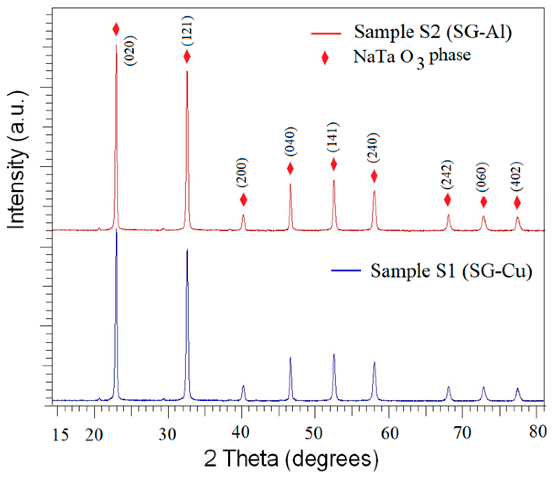
3.1. X-ray Diffraction Analysis

Figure 1 shows the X-ray diffraction patterns of the sodium tantalate samples doped with Cu and Al metal ions.
From Figure 1 it is observed that the XRD patterns of the samples are similar and they present the diffraction peaks corresponding to the well crystallized single phase NaTaO3 (JCPDS 73-0878). The X-ray diffraction data (Figure 1) allowed a good determination for the full width at half maximum (FWHM), β, of several diffraction maxima that present sufficient width: (020), (121), (040), (141) and (240), thus being able to calculate the average crystallite diameter of samples using the Debye–Scherrer equation. The results are listed in Table 1.
The X-ray powder diffraction spectra of SG-Al and SG-Cu samples were indexed using the EXPO2009 computer program (Version 2009) [27], leading to the lattice parameters shown in Table 1, the results are consistent with the space group Pcmn (space group number 62), belonging to the orthorhombic crystallographic family. At the same time, in Table 1 we presented the values of the lattice parameters for undoped NaTaO3, obtained with the VESTA program. It can be observed that by introducing Cu and Al dopant ions, the lattice parameters change, which proves the presence of dopants in the crystalline lattice. The values obtained for the lattice parameters are very close to those obtained by other authors [28].

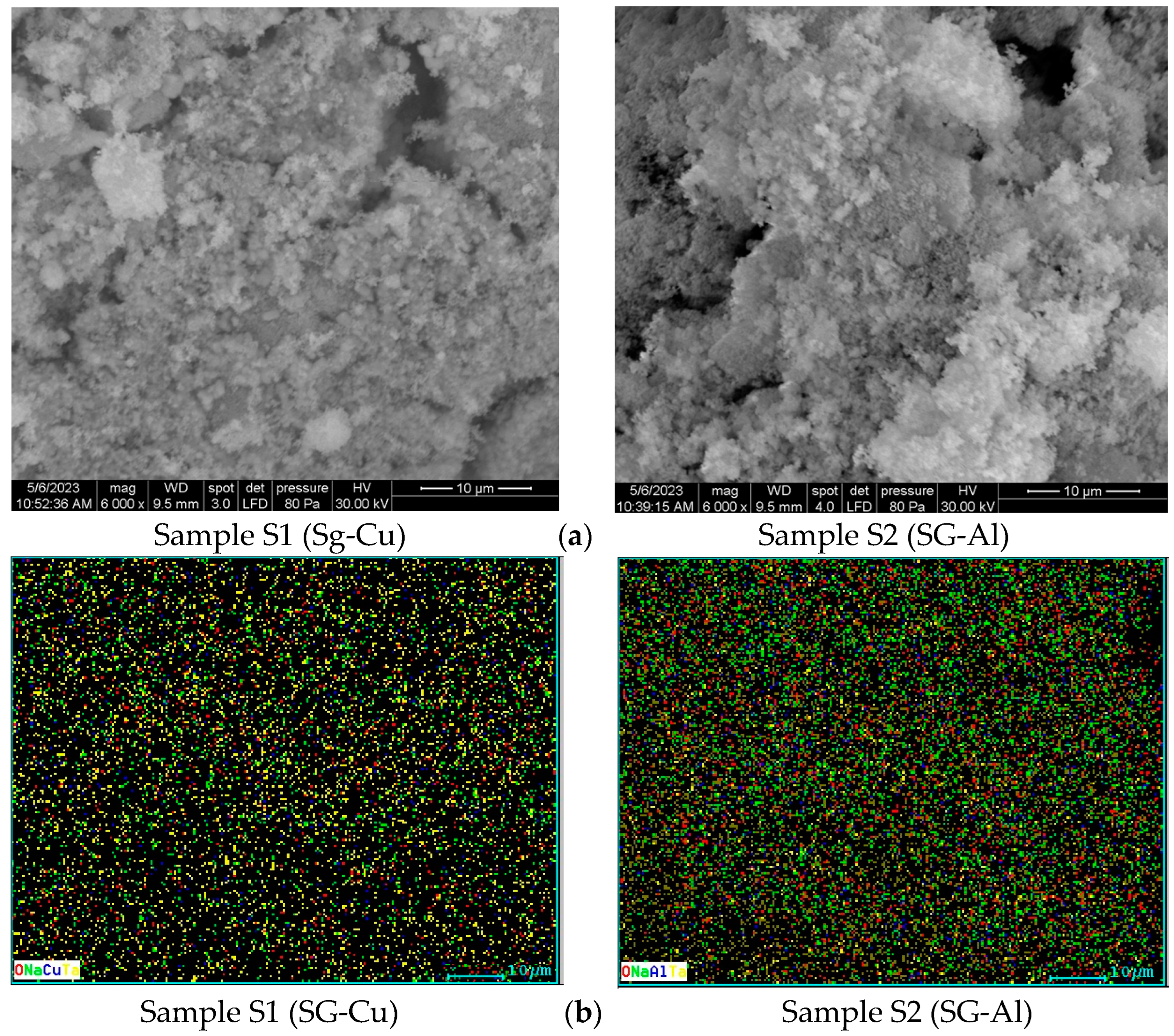
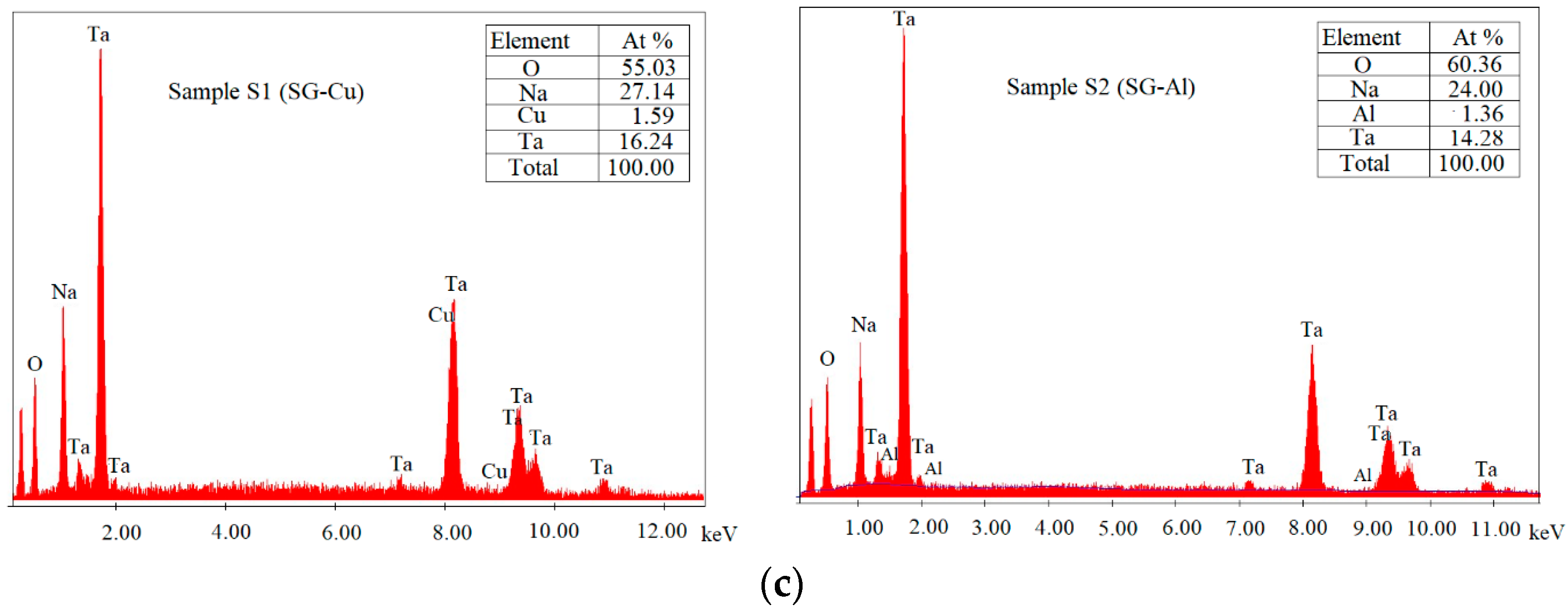
3.2. Scanning Electron Microscopy

The SEM images, the EDX spectrum, elements quantification and mapping of the Al or Cu doped NaTaO3 ceramic materials synthesized by sol-gel method, are shown in Figure 2.
From the SEM images of samples (Figure 2a), one can observe that for both samples the particles have a spherical shape, with dimensions of hundreds of nanometers, and are strongly agglomerated. Also, element’s mapping (Figure 2b) revealed uniform distribution of all present elements: O, Na, Ta and metal ions used as dopant (Cu or Al).

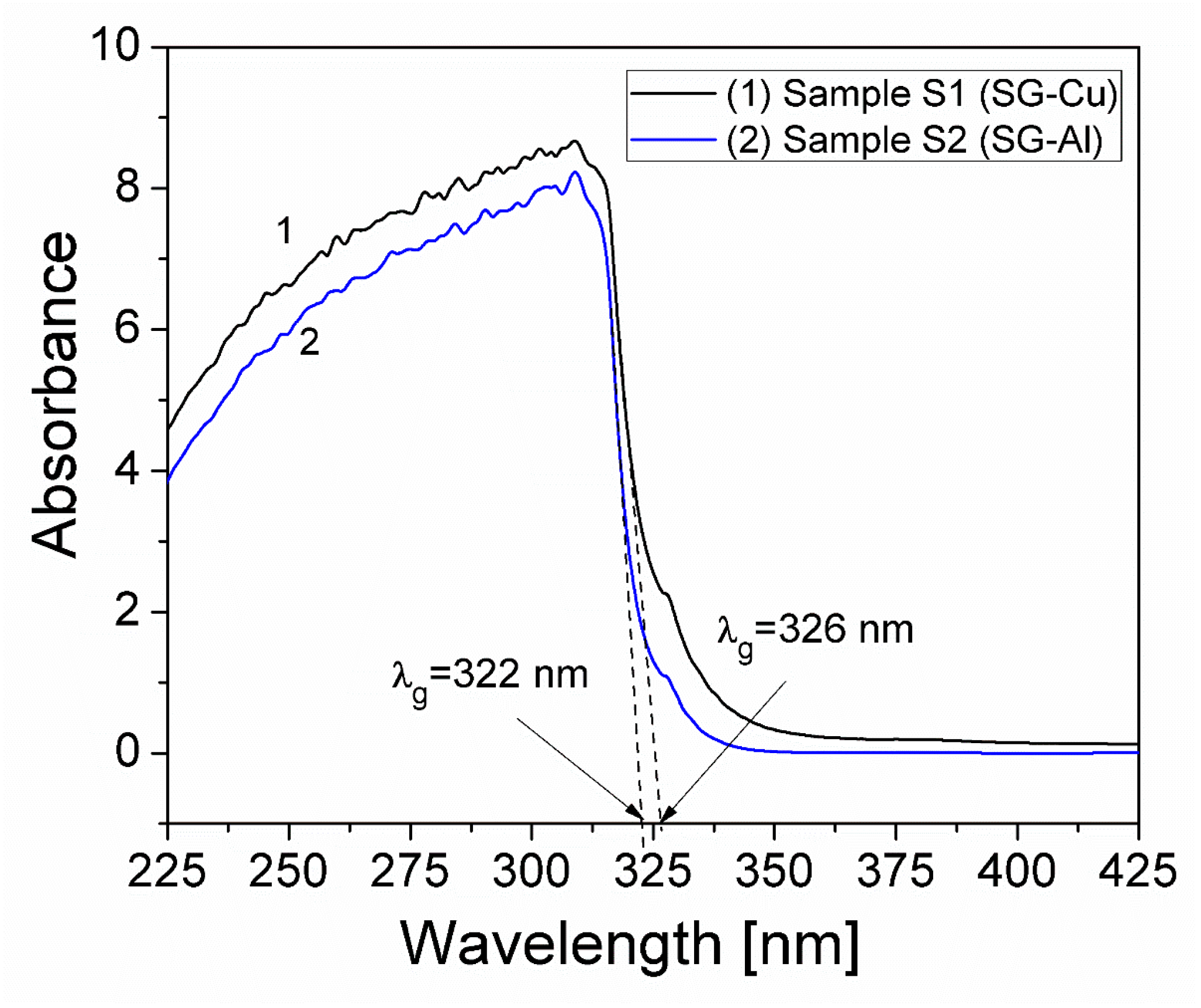
3.3. UV-VIS Spectroscopic Analysis

Figure 3 shows the UV-VIS absorption spectra of the samples. The wavelength λg, at the end of the absorption range was determined as the intersection between the wavelength axis and the tangent line drawn on the absorption spectrum. As can be seen from Figure 3, the λg values of the two samples are λg = 326 nm for sample S1 (Sg-Cu) and λg = 322 nm for sample S2 (SG-Al). Using the Kubelka–Munk method [29], the values of λg from Figure 3 and Equation (1), the values of the band gap energy (Eg) of the investigated samples, were computed [30].
E g ( e V ) = 1240 λ g ( n m )
The obtained values are Eg = 3.80 eV for sample S1 (SG-Cu) and Eg = 3.85 eV for sample S2 (SG-Al), which is smaller than the value reported in Ref. [30] (i.e., 4 eV) for a NaTaO3 obtained by the hydrothermal method. Therefore, the presence of the dopants (Cu or Al) in the structure of NaTaO3 leads to a decrease in the band gap energy, Eg, which can be useful for photocatalysis. The obvious decrease of the band gap energy (Eg) compared to that of pure NaTaO3, demonstrates an improved absorption in the visible (infrared) light range, and an increase in carrier mobility for each doped structure [31]. Studies have shown [31,32] that NaTaO3 is the first semiconductor photocatalyst that produces infrared absorption when doped with metal cations, which leads to a decrease in the band gap energy. At the same time, doping with metal ions reduces the rate of electron-hole recombination and consequently the population of charge carriers in the equilibrium state increases [32].

3.4. Electrical Properties

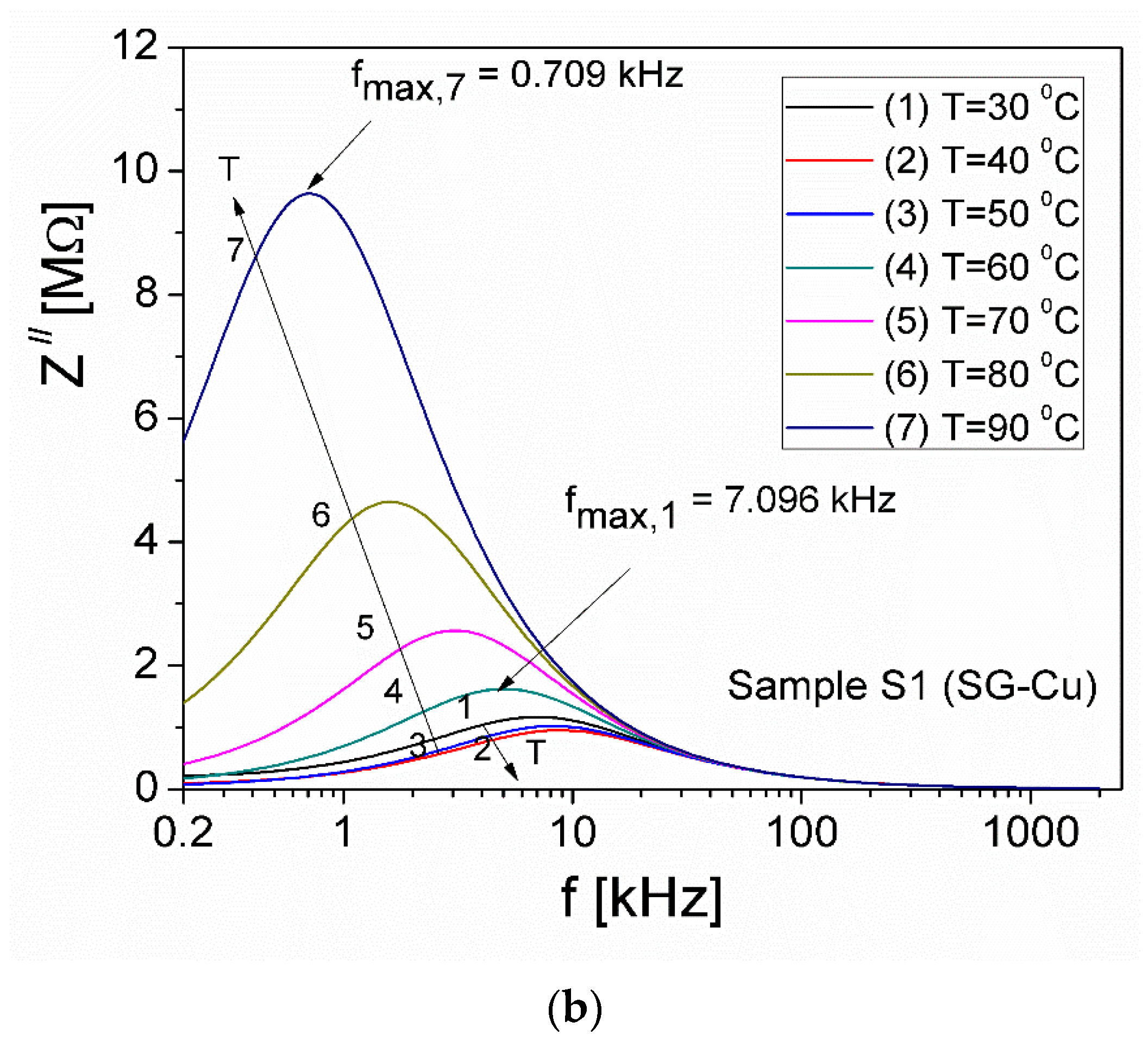
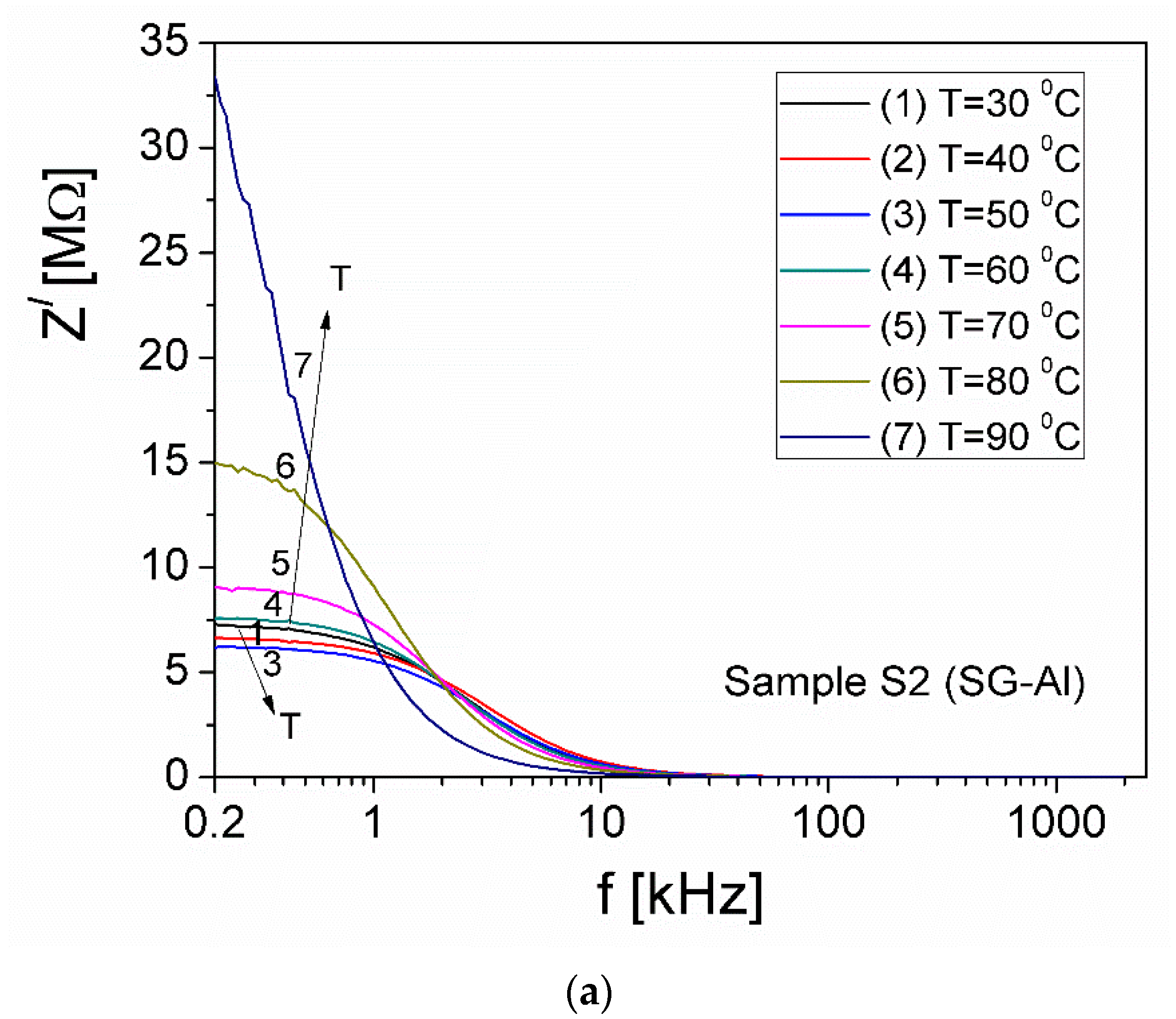
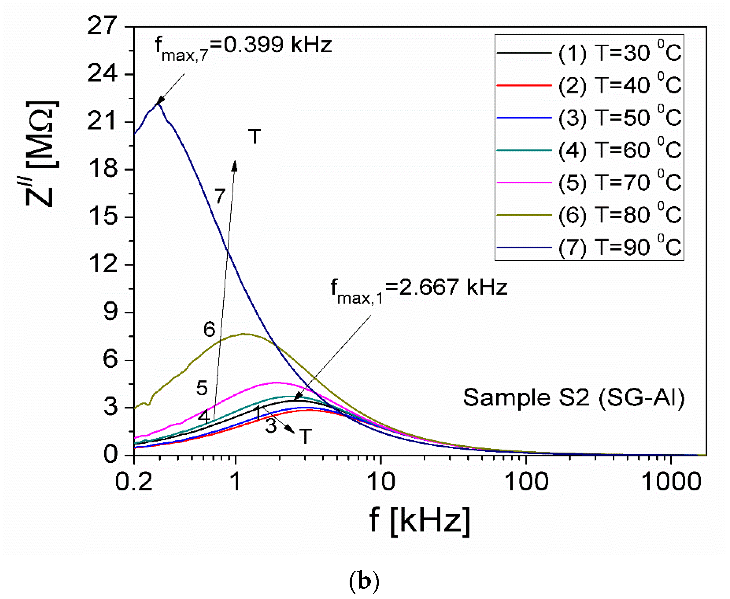
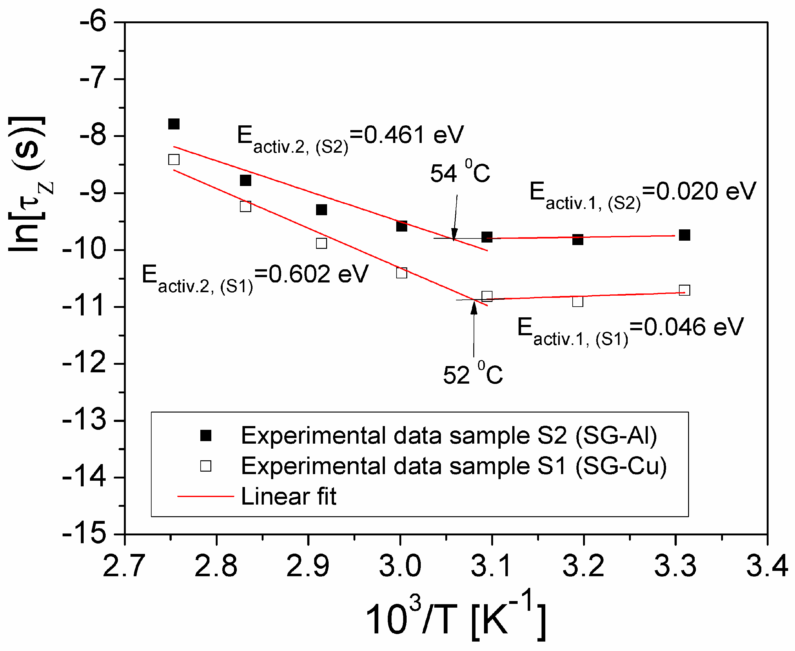
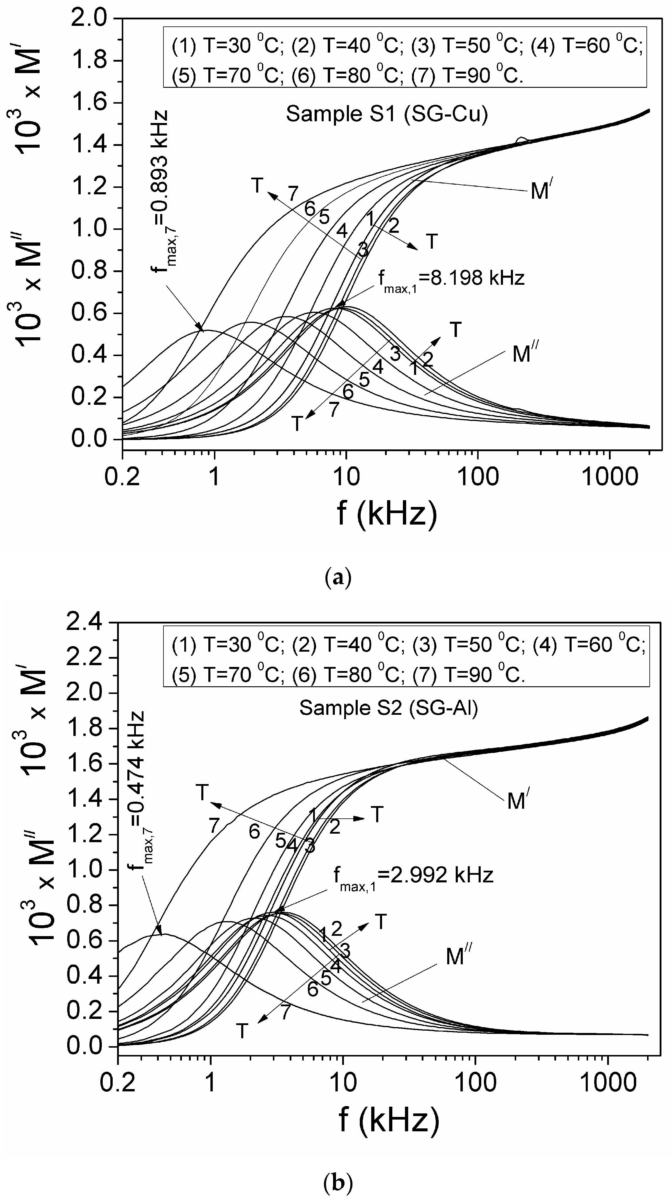
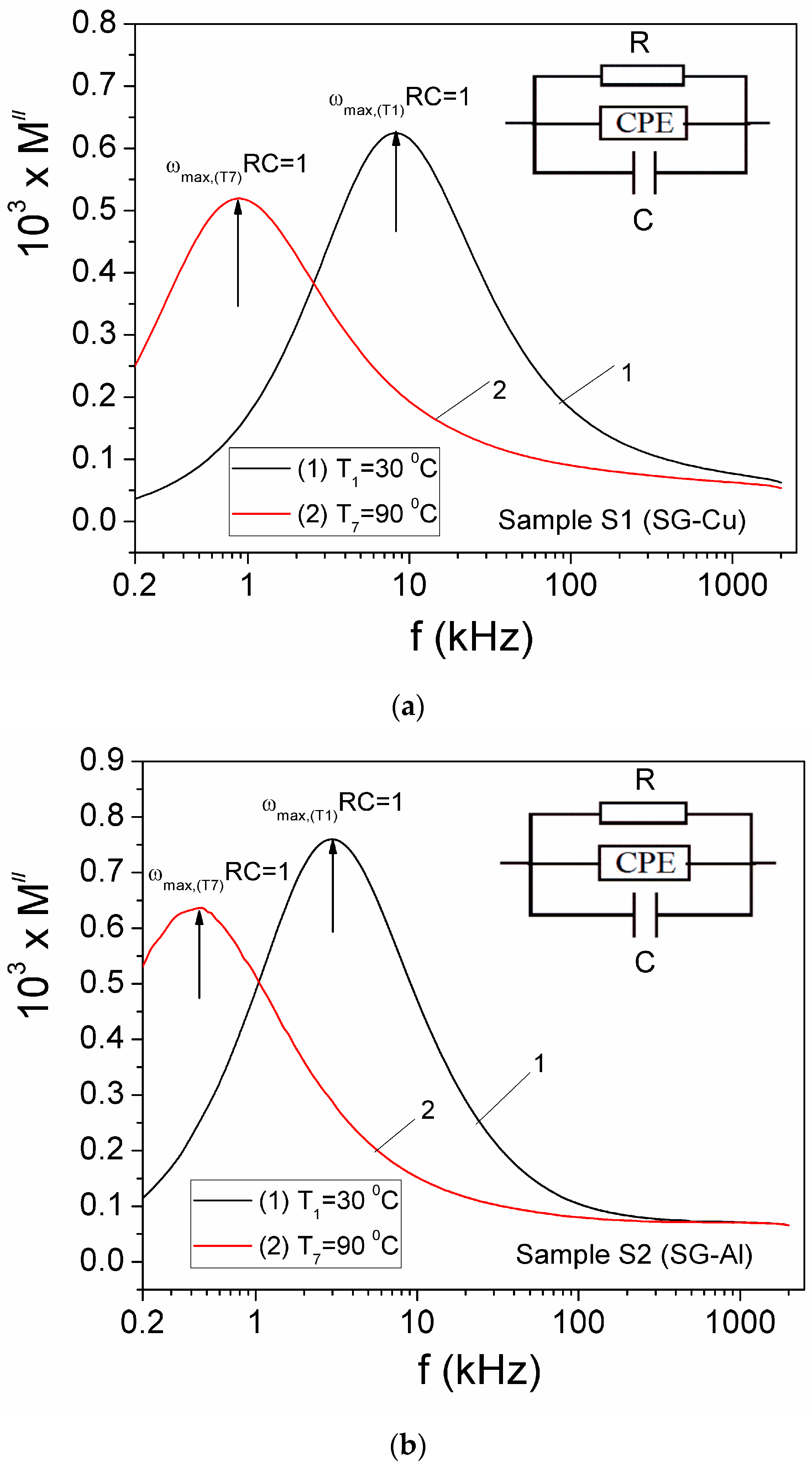
3.4.1. Complex Impedance

The frequency and temperature dependencies of the Z′ and Z″ components of the complex impedance of the samples, in the frequency range 200 Hz–2 MHz and at different temperatures between 30 and 90 °C are shown in Figure 4 for sample S1 (SG-Cu) and in Figure 5 for sample S2 (SG-Al).
As can be seen from Figure 4a and Figure 5a, for a constant temperature T, the real component Z′ of the complex impedance decreases with increasing frequency, for both samples. At low frequencies, between 200 Hz and 600 Hz, by increasing the temperature up to about 40–50 °C, it is observed that Z′ decreases slightly, then starts to increase significantly, up to values of 18 MΩ for sample S1, SG-Cu and up to 33 MΩ for sample S2, SG-Al, by increasing the temperature in the range 50–90 °C.
From Figure 4b and Figure 5b one can be observe that the imaginary component Z″ presents a maximum at frequency fmax,Z for both samples and for all investigated temperatures. For both samples, fmax,Z shifts towards higher values when the temperature increases up to approximately 50–60 °C, after which the temperature continues to increase up to 90 °C, fmax,Z moves towards smaller values.
This behavior of Z″ may be due to the perovskite-type structure of the two samples, highlighting the existence of an electrical relaxation process [33], which is due to the presence of charge carriers in the investigated samples [34,35]. The relaxation process is determined by the hopping of the charge carriers between localized states, according to the VRH model of Mott and Davis [34]. Based on the experimental values, fmax,Z from Figure 4b and Figure 5b, and on the Debye equation, τZ = ½πfmax,Z [36], we computed the relaxation times τZ, of the two samples at each temperature T. The variation of the relaxation time τZ, over the measurement temperature intervals, agrees with an Arrhenius type law:
τ Z = τ 0 exp E a c t i v . k T
where, τ0 represents the pre-exponential factor of the relaxation time; k is the Boltzmann’s constant and Eactiv. is the activation energy or the barrier energy between the localized states [34,37].
Figure 6 shows the plot of the experimental dependence, ln(τZ), on (103/T) for the investigated samples. The linear fit of the curves in Figure 6 provides two different slopes for each sample, which correspond to the two temperature ranges: below 52 °C and above 52 °C (for sample S1) and below 54 °C and above 54 °C (for sample S2), respectively. These temperature dependencies of τZ could be associated with two ranges of different electrical conductivity of the samples [38]. From the fitting with a straight line, of equation y = a + bx, where a is the intercept and b is the slope of the line, we determined the values of the activation energy, Eactiv., of samples S1 and S2, corresponding to the two temperature ranges. The obtained values are 0.046 eV (below 52 °C) and 0.602 eV (above 52 °C) for sample S1 (SG-Cu) and 0.020 eV (below 54 °C) and 0.461 eV (above 54 °C) for sample S2 (SG-Al), respectively. As a result, it can be stated that for the samples of NaTaO3 doped with Cu and Al ions respectively, we highlighted for the first time a transition from a semiconductor-like behavior to a conductor-like behavior, at a temperature of 52 °C for sample S1 (SG-Cu) and a temperature of 54 °C for sample S2 (SG-Al) respectively, where the change in the activation energy, Eactiv., also appears (see Figure 6).

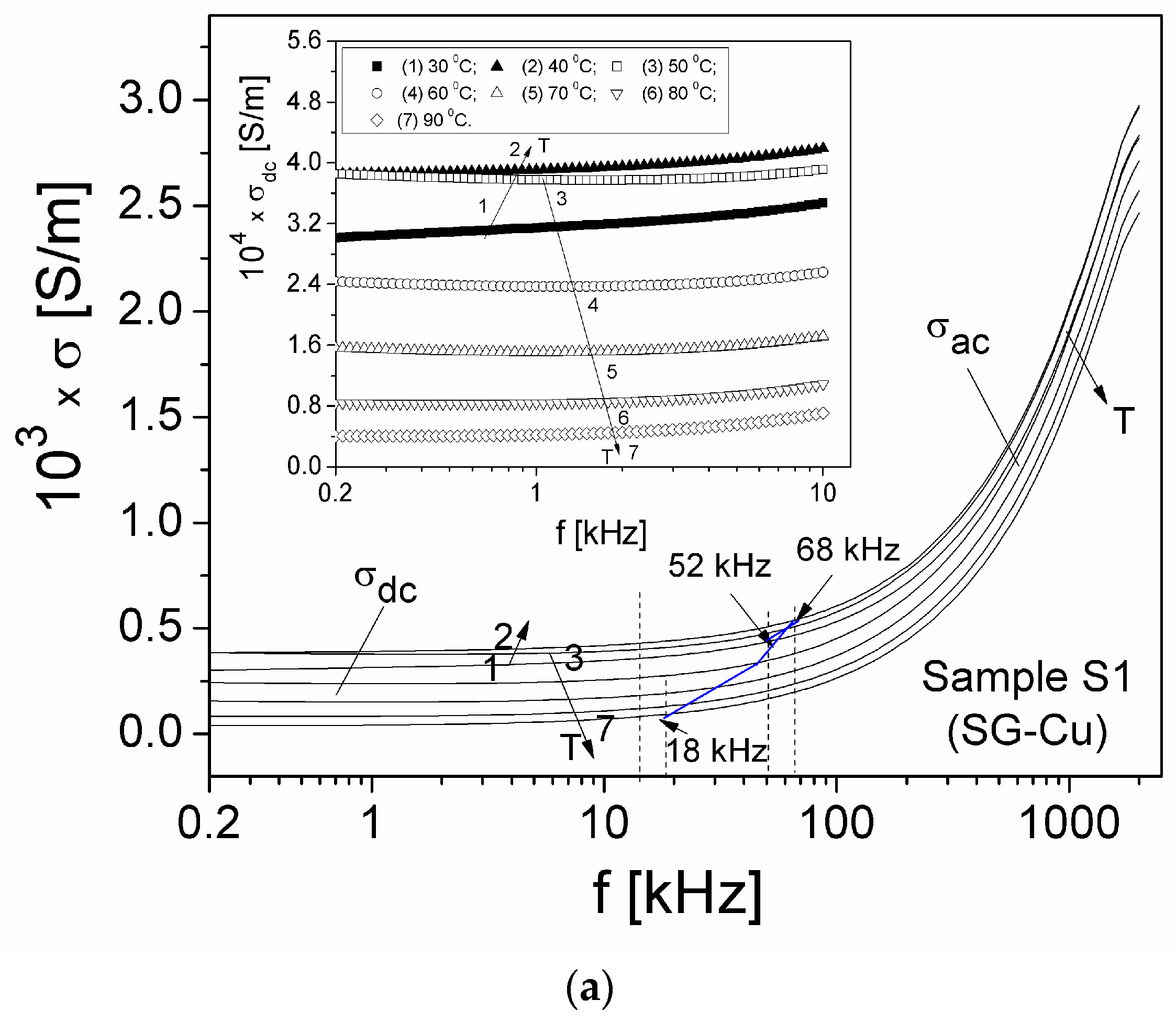
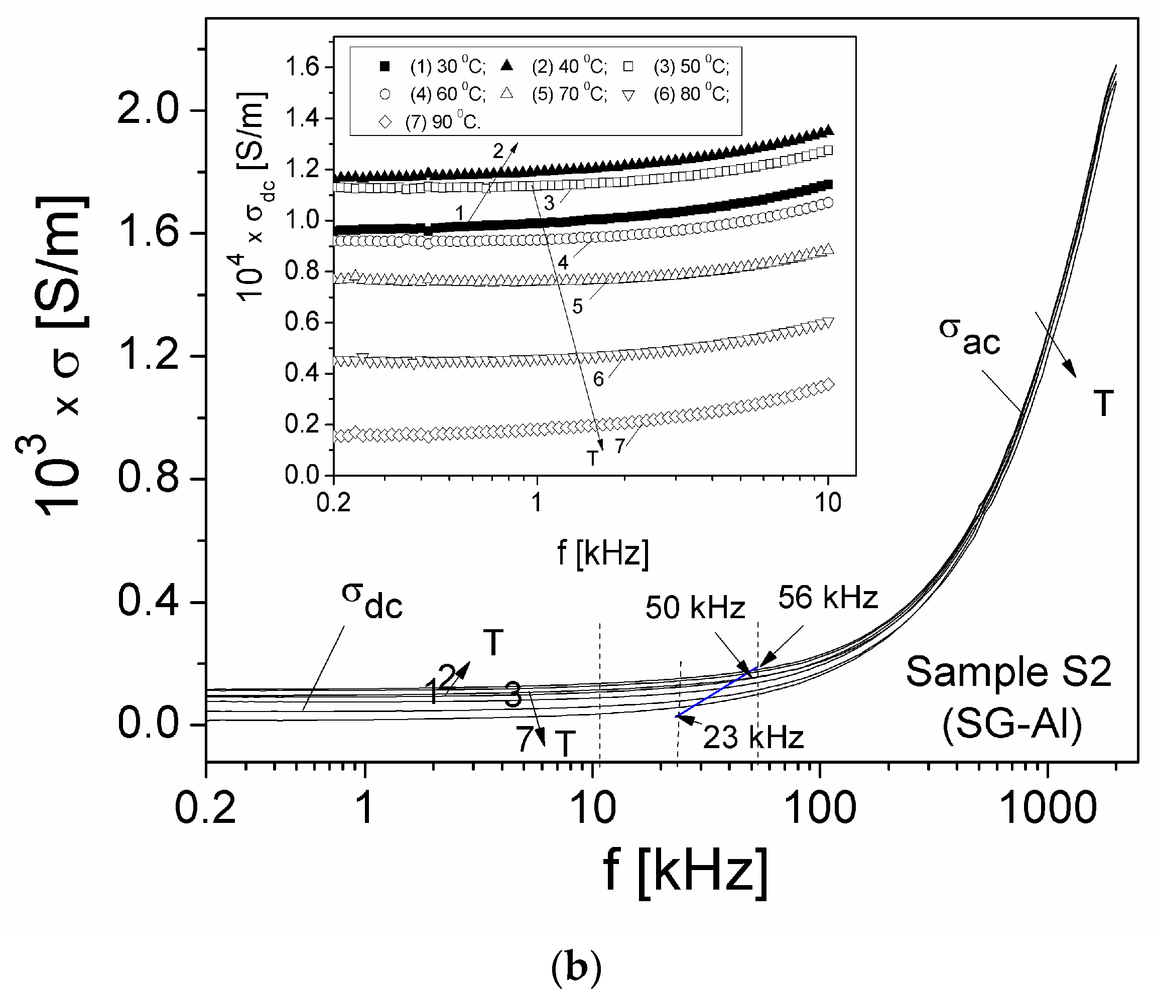
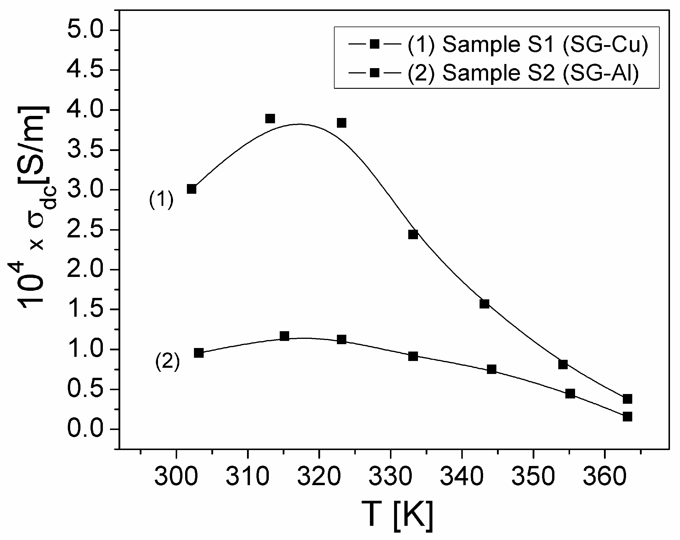
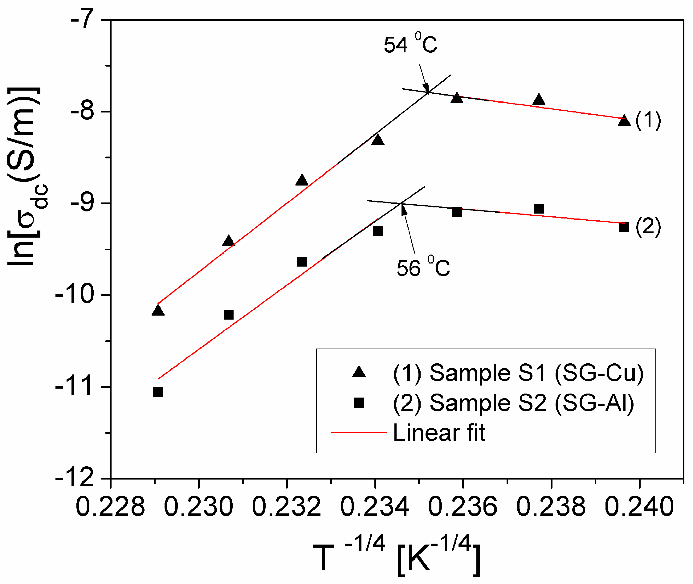
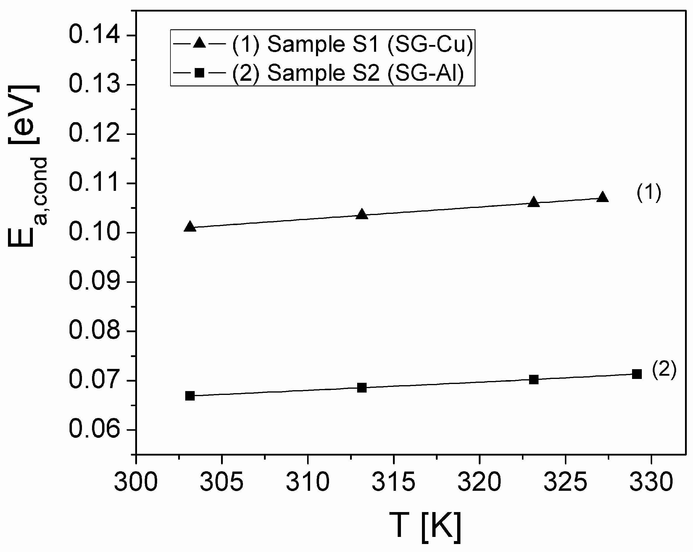
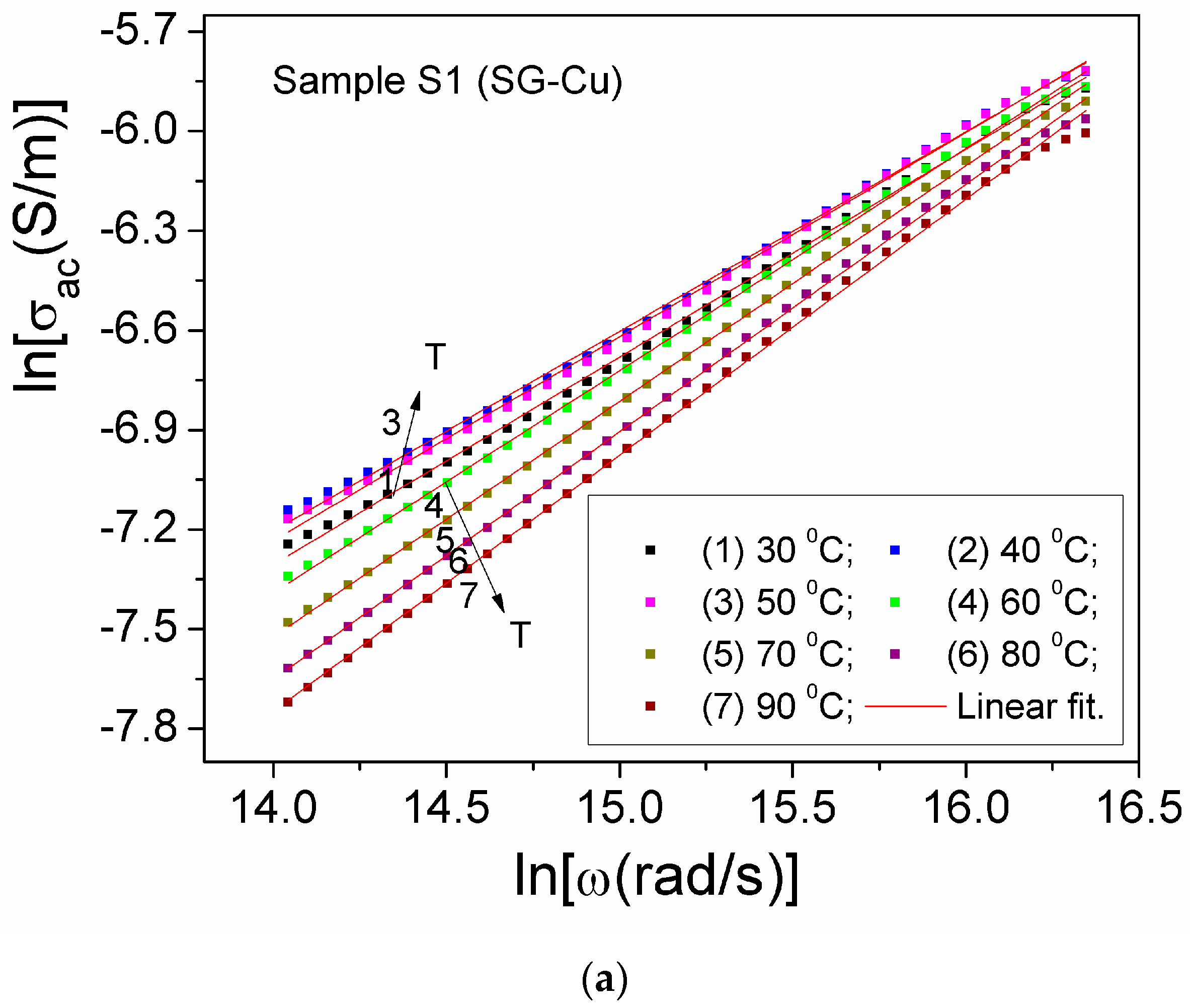
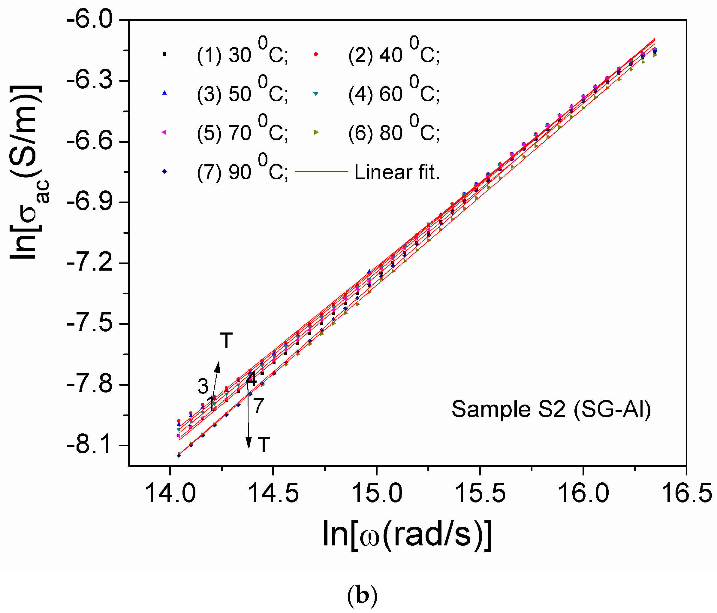
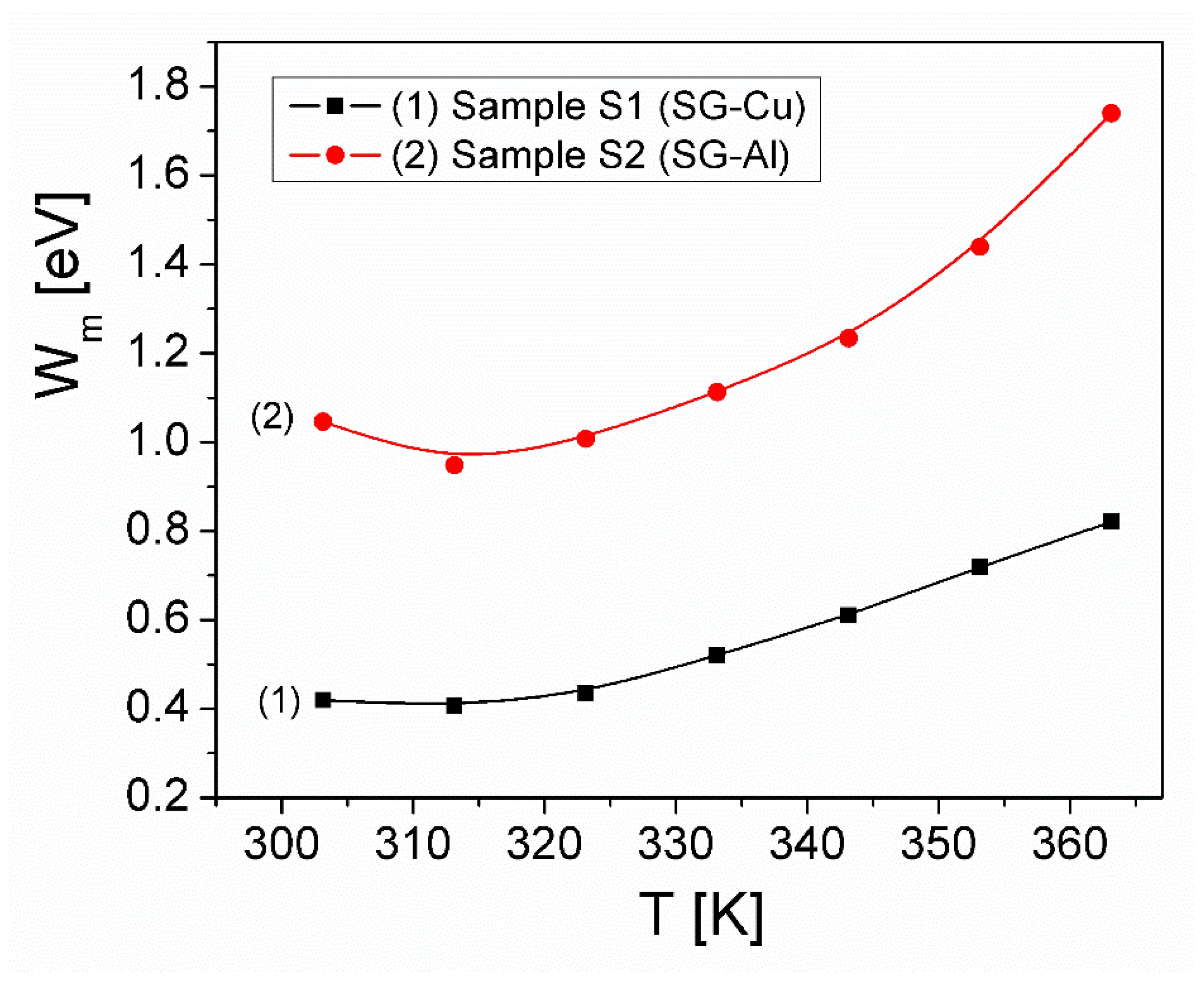
3.4.2. DC and AC Conductivity

Using the experimental values of the Z′ and Z″ components of the complex impedance of the samples (Figure 4 and Figure 5), we computed the electrical conductivity σ, with the relation:
σ = d A Z Z 2 + Z 2
where d is the thickness of sample and A is its cross-sectional area.
The frequency dependence of the conductivity, σ, of the investigated samples over the frequency range (200 Hz–2 MHz) and at different temperatures between 30 and 90 °C, is shown in Figure 7a for sample S1 (SG-Cu) and Figure 7b for sample S2 (SG-Al), respectively.
As can be seen from Figure 7, for each sample, the conductivity consists of two components according to Jonscher’s theoretical model [39], where the total conductivity is given by the equation:
σ ( ω , T ) = σ d c ( ω , T ) + σ a c ( ω , T )
The component denoted by σdc is called static conductivity (or DC conductivity) and the second component denoted by σac is called dynamic conductivity (or AC conductivity). At the same time, from Figure 7a,b it can be observed that σdc remains nearly constant for each temperature, T, up to the frequency of approximately 10 kHz, after which a rapid increase follows for both samples. In the inset of Figure 7a,b, the frequency dependence of σdc, over the range 200 Hz−10 kHz and at different temperatures between 30 and 90 °C is presented. Based on the values obtained for the static conductivity, σdc, from Figure 7a,b, at every temperature, T, at which the measurements were performed, we plotted the temperature dependence of the static conductivity, σdc(T), for both samples, as shown in Figure 8.
From Figure 8, it is observed that σdc(T), increases when the temperature increases from 30 °C to approximately 50 °C, then decreases with the increase in temperature from 50 °C to 90 °C, this behavior agrees with the VRH theory of Mott [34]. The increase in conductivity, σdc, in the region of low temperatures, between 30 and 50 °C, corresponds to semiconductor type behavior. This increase can be attributed to the increase in the drift mobility of electric charge carriers, which are thermally activated when the temperature increases [33]. As a result, it can be highlighted that, around the temperature of 50 °C, there is a transition from a semiconductor-type behavior to a conductor-type behavior in the investigated samples. At temperatures above 50–60 °C, the static conductivity decreases with the increase in temperature, indicating that the samples behave like conductors [40].
For both investigated samples, over the temperature range 30–50 °C, where they have a semiconductor-type behavior, based on Mott’s VRH model [34], the temperature dependence of the static conductivity, σdc is given by the equation:
σ d c = σ 0 exp D T 1 / 4
In Equation (5), σ0 is the pre-exponential factor with dimensions of Ω−1m−1 and D is given by the relation:
D = 4 E c o n d k T 3 / 4
Figure 9 shows the experimental dependence ln(σdc)(1/T1/4), for the two samples at low frequencies. The linear fit of the curves in Figure 9, corresponding to both sample S1 (SG-Cu) and sample S2 (SG-Al), shows that the slope of the conductivity changes at T = 54 °C (for sample S1) and at T = 56 °C (for sample S2). This result is in agreement with the variation of the relaxation time, τZ with temperature, shown in Figure 6, which was associated with two ranges of different electrical conductivity of the samples. Thus, the result obtained in Figure 9, highlights once again the fact that the temperatures of 54 °C for sample S1 (SG-Cu) and 56 °C for sample S2 (SG-Al), represent the transition temperature from a semiconductor-type behavior to a conductor-type behavior, also taking place a change of the activation energy of conduction, Ea,cond, of the samples, as we also obtained in Figure 6. At the same time, by increasing the temperature to approximately 50–60 °C, the doping ions of Cu and Al, respectively, induce in the NaTaO3 structure, a transition from the semiconductor-like to conductor-like behavior of the TaO compounds [41]. Considering the paper [41], we can say that in the case of NaTaO3 samples doped with Cu ions (sample S1) and respectively with Al ions (sample S2), Cu-Ta and Al-Ta bonds are formed on the TaO surface, which introduce holes as the main charge carrier and, consequently, the Fermi level is shifted into the valence band, where electronic states are now populated. As a result, it can be said that in the analyzed samples a metallic transition takes place at a temperature located between 50 and 60 °C, called transition temperature, thus highlighted for the first time in perovskite compounds of this type.
From the straight-line fitting of the experimental dependence, ln(σdc)(1/T1/4), from Figure 9, for each sample, we determined the slope D, corresponding to the interval (30–54 °C), for sample S1, and for the temperature range (30–56 °C) for sample S2, respectively, in which the samples show a semiconductor-like behavior. Then with the relation Equation (6) we computed the activation energy of conduction, Ea,cond(T), for each sample. Figure 10 shows the temperature dependence Ea,cond(T), for the S1 (SG-Cu) and S2 (SG-Al) samples.
From Figure 10, it can be seen that Ea,cond increases linearly with temperature, for both samples, from 0.101 eV to 0.107 eV for sample S1 (SG-Cu) and from 0.067 eV to 0.071 eV for sample S2 (SG-Al). The mechanism of the electrical conductivity in the investigated samples at low frequencies can be explained by the hopping process of the charge carriers between the localized states [42] over the temperature range between 30 °C and approximately 54–56 °C, based on the Mott VRH model. The obtained values are similar to the values obtained in Ref. [22] for the activation energy of the conduction process for NaTaO3 samples doped with Fe or Ag ions.
As we showed in Ref. [43], taking into account Mott’s VRH model and the values obtained for the activation energy of the conduction process, Ea,cond(T), we established Equation (7), which allows the determination of the density of localized states at the Fermi level, N(EF):
N ( E F ) = λ ( a k T ) 3 ( 4 E a , c o n d ) 4
where λ ≈ 16.6, is a non-dimensional constant and a ≈ 109 m−1 is the degree of localization [34]. Using Equation (7) and the values of Ea,cond(T), from Figure 10, we have computed N(EF) at temperatures below 50–60 °C for both samples. The following values were obtained for the first time for NaTaO3 ceramic samples doped with Cu or Al metal ions: N(EF) = 4.45 × 1019 cm−3⋅eV−1 for sample S1 (SG-Cu) and N(EF) = 23.12 × 1019 cm−3⋅eV−1 for sample S2 (SG-Al), and these do not depend on temperature for the investigated temperature range. Similar results, where N(EF) remains constant throughout the investigated temperature range, were also obtained for other materials, such as: vivianite [40] or crednerite [44] materials.
From the values obtained for the density of localized states at the Fermi level of the two samples, it is observed that N(EF) for sample S2 (SG-Al) is higher than N(EF) for sample S1 (SG-Cu). The result is in agreement with the decrease of DC conductivity, σdc of sample S2 compared to σdc of sample S1 (see Figure 8), i.e., the decrease of the activation energy for electrical conduction, Ea,cond (see Figure 10) leads to an increase of the density of states at the Fermi level N(EF). We consider that this increase in N(EF) could be correlated with a decrease in the hopping distance between the localized states of the charge carriers. To justify this statement, we determined two other Mott’s parameters of the VRH model: the hopping distance R and the hopping energy W, with these equations [34]:
R = 9 8 a k T N ( E F ) 1 / 4
W = 3 4 π R 3 N ( E F )
Using the N(EF) values of samples S1 and S2, and the Equations (8) and (9), we determined the hopping distance, R, and the hopping energy, W, at different temperatures for the investigated samples. The values obtained are indicated in Table 2.
As can be seen from Table 2, for both samples, the hopping distance, R, decreases with increasing temperature and the hopping energy, W, increases with increasing temperature. Also, the hopping distance, R, and the hopping energy, W, corresponding to sample S2 (SG-Al) are smaller than R and W corresponding to sample S1 (SG-Cu) for the same temperature, T. This result confirms our previous statement regarding the increase in density states at the Fermi level N(EF) of sample S2 (SG-Al) compared to N(EF) of sample S1 (SG-Cu), due to the decrease of the hopping distance R(S2) compared to R(S1).
In the dispersion region corresponding to high frequencies (Figure 7a,b), the dynamic conductivity, σac(ω,T), respects the equation [39]:
σ a c ( ω , T ) = A 0 ( T ) ω n ( T )
where n is a temperature-dependent exponent (0 < n < 1) and A0 is a pre-exponential factor that depends on temperature [39]. By taking the logarithm of Equation (10), a linear dependence between lnσac and lnω is obtained. Figure 11a,b shows the experimental dependence of ln(σac) on ln(ω) for samples S1 (SG-Cu) and S2 (SG-Al) at each temperature T.
By fitting the experimental dependence ln(σac)(ln(ω)), from Figure 11 with a straight line, the exponent n and the parameter A0, corresponding to each sample at every temperature, T, can be determined and the obtained values are listed in Table 3.
From Table 3, it can be observed that in the case of sample S2 of NaTaO3 doped with Al ions, the exponent n has relatively high values (over 0.7), at all temperatures T over the investigated range, while in the case of sample S1 of NaTaO3 doped with Cu ions, high values for the exponent n (over 0.7) are obtained only when the temperature increases above 70 °C. The relatively high values obtained for the exponent n (over 0.7), show that in the investigated samples the phenomenon of electrical conduction at high frequencies (f > 100 kHz) is due to a hopping process of the charge carriers from samples between the nearest neighboring states, according to the CBH (correlated barrier hopping) model [35,45], which in the case of sample S1 of NaTaO3 doped with Cu ions is present only at high temperatures, above 70 °C. At the same time, this result can also be correlated with the fact that the activation energy for conduction Ea,cond obtained for sample S1 (SG-Cu) is higher than the activation energy for conduction Ea,cond obtained for sample S2 (SG-Al), as shown in Figure 10. The exponent n in a first approximation, based on CBH model can be written as:
n = 1 6 k T W m
In Equation (11) Wm represents the maximum energy barrier height (or band gap energy) [45,46] and can be calculated using Equation (11) and the n values of the two samples (Table 3) corresponding to each temperature T. The temperature dependence of the maximum energy barrier height, Wm(T), is shown in Figure 12 for the two samples.
From Figure 12 it can be seen that the addition of metal ions of Al or Cu in the structure of the NaTaO3 perovskite compound leads to a decrease in the energy of the band gap, up to temperatures of 40–50 °C, after which Wm starts to increase with the increase in temperature, up to 90 °C, tending to values of 0.75 eV for sample S1 (SG-Cu) and 1.74 eV for sample S2, approaching the bandgap energy value of the un-doped NaTaO3 material, which has values between 1 and 3 eV [17,47]. According to Jonscher’s theoretical model [39], the total conductivity given by Equation (4), can also be written in the following form:
σ ( ω , T ) = σ d c 1 + ω ω h n
Based on Equations (10) and (12), the expression of ωh results immediately. It represents the hopping frequency [37,39], i.e., the frequency of transition from the DC regime to the dispersive regime AC, of the electrical conductivity.
ω h = σ d c A 0 1 / n
The obtained values for ωh are shown in Table 3. In Figure 7a,b, the hopping frequencies (fh = ωh/2π), are indicated at which the transition from the DC regime to the AC regime occurs. The results show that by increasing the temperature from 30 °C to 50 °C, fh, increases slightly for both samples (see Figure 7), after which it decreases until at 18 kHz (sample S1) and 23 kHz (sample S2), when the temperature increases up to 90 °C. It is known that the mechanisms of electrical conduction in materials can be investigated based on the electrical modulus, M = M′ − iM″, where the real (M′) and imaginary (M″) components can be determined with the relations [48]:
M = ω ε 0 A d Z
M = ω ε 0 A d Z
In these relationships, ε0 is the free space dielectric permittivity. Using Equations (14) and (15) and the Z′ and Z″ values from Figure 4 and Figure 5, we determined the components M′ and M″ of the electrical modulus for the two samples. Figure 13 shows the frequency dependence of the M′ and M″ components at all investigated temperatures, T, for both sample S1 (SG-Cu) (Figure 13a) and sample S2 (SG-Al) (Figure 13b).
From Figure 13 it can be seen that for each temperature, by increasing the electric field frequency, the M′ component increases continuously and tends to a constant value of approximately 1.5 (for sample S1) and 1.8 (for sample S2). At the same time, for a constant frequency, the value of M′ decreases slightly with the increase in temperature up to approximately 50 °C, after which it starts to increase when the temperature increases from 50 °C to 90 °C. This behavior can be attributed to the temperature-dependent relaxation process in the investigated samples [49]. The imaginary component M′′ presents a maximum for each temperature, corresponding to a frequency, fmax,(M) (see Figure 13a,b). Using the values fmax,(M) and Debye equation, we have computed the relaxation times τM, corresponding of each temperature. The obtained values are listed in Table 4.
It is known [48,50] that in the case of ideal samples placed in a capacitive cell connected to the terminals of an RLC-meter of variable frequency, the equivalent electrical circuit of the cell is a parallel circuit formed by the capacity C and the resistance R, of the sample material between the capacitor plates. On the other hand, to estimate the electrical properties of a material with dielectric losses, the equivalent electrical model includes the RQC circuit, associated with the grain intake: the grain resistance (Rg), the grain capacity (Cg) and the constant phase element (CPE), which is introduced due to the non-ideal capacitive behavior of the material in the measuring cell [51]. Besides the deviation from the ideal Debye behavior [50], the presence of the constant phase element (CPE) in the equivalent circuit of the investigated material is correlated with the Jonscher characteristic of universal power law (see Equations (4) and (10)) which plays an important role in the investigation of the electrical properties of the material [20]. As shown in Refs. [51,52], the constant phase element “Q” can be calculated from Equation (16), where the parameter n is the same as that obtained from AC-conductivity measurements (n < 1), which are indicated in Table 3. For an ideal resistor and ideal capacitor (with a Debye-type behavior), n = 1 (for ideal capacitor) and n = 0 (for ideal resistor) [20].
C = R 1 n Q 1 / n
At the same time, the relaxation time τM can be defined in terms of resistance (R) and capacity (C) with the relation, τM = RC, so that the Debye equation is written in the form, 2πfmaxRC = 1. The estimation of the R and C values of the equivalent electric circuit can be accomplished both by graphically representing the temperature dependence M″(f) for two values of the temperature T (the minimum value T1 = 303 K and the maximum, T7 = 363 K), and by the equivalent parallel (RQC) circuit (Figure 14).
The elements R and C of the parallel circuit influence the shape of the M″(f) peaks (Figure 13) and the amplitude of the peak in the M″(f) curves is proportional to the capacity C, i.e., Mmax = C0/2C where C0 is cell capacity without sample (C0 = 0.0115 pF). Knowing the Mmax (Figure 13) and τM values (Table 4), both the elements Cg and Rg of the equivalent parallel circuit, corresponding to the samples, at each temperature, T, were determined. The obtained values are shown in Table 4. The constant phase element “Q” can be computed from Equation (16) taking into account the values of Rg, Cg (Table 4) and n (Table 3) corresponding to samples S1 (SG-Cu) and S2 (SG-Al). The values obtained for the phase element constant “Qg” are indicated in Table 4.
As seen from Table 4, by increasing the temperature T from 30 °C to 90 °C, the grain capacity Cg of the equivalent electric circuit of the two samples increases from 8.8 pF to 10.6 pF (for sample S1 (SG-Cu)), respectively from 7.8 pF at 9.4 pF (for sample S2 (SG-Al)). This behavior is observed in most ferrites [33,53,54]. By increasing the temperature, the thermal activation of the hopping of charge carriers in the octahedral sites takes place, this process is responsible for the electrical conduction in the samples [33]. As a result, the dielectric polarization increases, and therefore, the dielectric permittivity, which causes an increase in the capacity, C by increasing the temperature. Also, from Table 4, it is observed that by increasing the temperature from 30 °C to 90 °C, the grain resistance Rg of the equivalent electrical circuit increases from 2.20 MΩ to 16.8 MΩ (for sample S1 (SG-Cu)), respectively from 6.7 MΩ at 35 MΩ (for sample S2 (SG-Al)), this behavior is observed by other authors as well [55,56]. The increase in the resistance Rg of the equivalent electrical circuit of samples can be attributed to the increase in the mobility of charge carriers and their hopping rate with temperature [55]. At the same time, such materials that show a high resistance to temperature increase is characterized by low dielectric losses [55,56].

4. Conclusions

Two NaTaO3 ceramic samples in powder form, doped with Cu metal ions (sample S1) or with Al ions (sample S2), were prepared by the sol-gel method. X-ray diffraction analysis shows that both samples S1 (SG-Cu) and S2 (SG-Al) are well crystallized, without secondary phases and crystallize in the space group Pcmn (space group number 62), which belongs to the orthorhombic crystallographic family. The UV-VIS measurements show that the presence of Cu or Al ions in the NaTaO3 structure leads to a decrease in the optical band-gap energy (Eg) of the samples, obtaining values of 3.80 eV (for sample S1 (SG-Cu)) and 3.85 eV (for sample S2 (SG-Al)), which are lower than the value reported for a sample of NaTaO3 (4 eV). Complex impedance measurements, in the frequency range 200 Hz–2 MHz, and at different temperatures between 30 and 90 °C, in both samples, showed the presence of a maximum of the imaginary component Z″ of the complex impedance at each temperature T, thus, indicating the existence of an electrical relaxation process due to the hopping of charge carriers between localized states, according to Mott’s VRH model. These measurements allowed, for the first time, the determination of the activation energy, Eactiv., which represents the barrier energy between the localized states, associated with two zones of different conductivity. The following values were obtained for the two samples: 0.046 eV (below 52 °C) and 0.602 eV (above 52 °C) for sample S1 (SG-Cu) and 0.020 eV (below 54 °C) and 0.461 eV (above 54 °C) for sample S2 (SG-Al), respectively. Based on the obtained results, we highlighted for the first time a transition temperature from a semiconductor-type behavior to a conductor-type behavior, for the two samples: 52 °C (for sample S1 (SG-Cu)), respectively 54 °C (for sample S2 (SG-Al)), the temperature at which the change in the barrier energy between the localized states, Eactiv, of the samples also occurs. Using the complex impedance measurements, the spectrum of the electrical conductivity σ(f,T) of samples, was determined, and the results show that at all investigated temperatures, the conductivity σ for the samples follows Jonscher’s universal law. The temperature dependence of the static conductivity σdc(T) was determined and the results show that the slope of the static conductivity changes at the temperature of 54 °C (for sample S1) and 56 °C (for sample S2), another highlighting of the fact that the samples change their behavior from a semiconductor-type to a conductor-type. Using the Mott’s VRH model, the density of localized states at the Fermi level, N(EF), was determined for the first time on NaTaO3 ceramic samples doped with Cu or Al metal ions, obtaining the following values: N(EF) = 4.45 × 1019 cm−3⋅eV−1 (for sample S1 (SG-Cu)) and N(EF) = 23.12 × 1019 cm−3⋅eV−1 (for sample S2 (SG-Al)). These values do not depend on temperature for the investigated temperature range. The increase in the density of states at the Fermi level N(EF) of sample S2 (SG-Al) compared to N(EF) of sample S1 was explained by the decrease in the hopping distance, R, of charge carriers in sample S2 compared to that of sample S1. In the high frequencies region (over to 200 kHz), the band gap energy (Wm) of the both samples and the transition frequency ωh, from the DC regime to AC regime, at all investigated temperatures were determined, for the first time, based on the VRH and CBH models, for samples S1 (SG-Cu) and S2 (SG-Al). Taking into account the Jonscher characteristic of universal power law, an original method to evaluate the elements of the equivalent electrical circuit of the investigated samples, at different temperatures, was proposed: the grain resistance (Rg), the grain capacity (Cg) and the constant phase element (CPE). Knowing the electrical properties of NaTaO3 ceramic materials doped with Cu or Al metal ions at different frequencies and temperatures is useful for clarifying the electrical conduction mechanisms in these materials, as well as for their use in electronic applications, thermoelectric energy conversion or applications photocatalytic.

Author Contributions

Conceptualization, I.M. and C.N.M.; methodology, P.S.; software, C.N.M. and P.S.; validation, I.M., C.N.M. and P.S.; formal analysis, P.S.; investigation, I.M., P.S. and C.N.M.; resources, C.N.M. and I.M.; writing—original draft preparation, I.M.; writing—review and editing, C.N.M. and I.M.; visualization, I.M., P.S. and C.N.M.; supervision, I.M. and C.N.M. All authors have read and agreed to the published version of the manuscript.

Funding

This research received no external funding.

Data Availability Statement

The original contributions presented in the study are included in the article, further inquiries can be directed to the corresponding author.

Conflicts of Interest

The authors declare no conflicts of interest.

References

  1. Sun, C.; Alonso, J.A.; Bian, J. Recent Advances in Perovskite-Type Oxides for Energy Conversion and Storage Applications. Adv. Energy Mater. 2020, 2000459, 21. [Google Scholar] [CrossRef]
  2. AbuSandal, A.S.; Elhadi, M.M.; Suliman, A.H.; Elbadawi, A.A. Comparative study of electrical and optical properties of SrPrFeTiO6 double perovskite ceramic: A potential candidate for solar cells applications. IOSR J. Appl. Phys. (IOSR-JAP) 2022, 14, 16–24. [Google Scholar]
  3. Temerov, F.; Baghdadi, Y.; Rattner, E.; Eslava, S. A Review on Halide Perovskite-Based Photocatalysts: Key Factors and Challenges. ACS Appl. Energy Mater. 2022, 5, 14605–14637. [Google Scholar] [CrossRef]
  4. Bati, A.S.R.; Zhong, Y.L.; Burn, P.L.; Nazeeruddin, M.K.; Shaw, P.E.; Batmunkh, M. Next-generation applications for integrated perovskite solar cells. Commun. Mater. 2023, 4, 2. [Google Scholar] [CrossRef]
  5. Deshmukh, V.; Harini, H.; Nagaswarupa, H.; Naik, R.; Ravikumar, C. Development of novel Co3+ doped LaMnO3 perovskite electrodes for supercapacitors and sensors: Mechanism of electrochemical energy storage and oxygen intercalation. J. Energy Storage 2023, 68, 107805. [Google Scholar] [CrossRef]
  6. Park, Y.; Lee, J.-S. Metal Halide Perovskite-Based Memristors for Emerging Memory Applications. J. Phys. Chem. Lett. 2022, 13, 5638–5647. [Google Scholar] [CrossRef]
  7. Wang, D.; Zhang, C.; Zulfikar, A.J.; Mehrez, S.; Huynen, I.; Mahariq, I.; Elbadawy, I. Tuning layer thickness and layer arrangement in a GdMnO3 and GdMnO3-MoSe2 bi-layer absorber to cover the S, C, and X band frequency range. Surf. Interf. 2023, 36, 102507. [Google Scholar] [CrossRef]
  8. Singh, C.; Kumar, A. Investigation on ferroelectric, dielectric and pressure sensing properties of samarium substituted lead magnesium niobate-lead titanate oxide. Phys. B Cond. Matter 2023, 659, 414869. [Google Scholar] [CrossRef]
  9. Hoye, R.L.Z.; Hidalgo, J.; Jagt, R.A.; Correa-Baena, J.-P.; Fix, T.; MacManus-Driscoll, J.L. The Role of Dimensionality on the Optoelectronic Properties of Oxide and Halide Perovskites, and their Halide Derivatives. Adv. Energy Mater. 2022, 12, 2100499. [Google Scholar] [CrossRef]
  10. Rendón, R.C.; Salvo, C.; Sepúlveda, E.; Arulraj, A.; Sanhueza, F.; Rodríguez, J.J.; Mangalaraja, R.V. Evaluation of Structural and Functional Properties of La0.6Sr0.4MnO3 Perovskite Prepared by the Fast Solution Combustion Approach. Catalysts 2022, 12, 1636. [Google Scholar] [CrossRef]
  11. Park, Y.; Kim, S.H.; Lee, D.; Lee, J.S. Designing zero-dimensional dimer-type all-inorganic perovskites for ultra-fast switching memory. Nat. Commun. 2021, 12, 3527. [Google Scholar] [CrossRef]
  12. Choi, J.; Han, J.S.; Hong, K.; Kim, S.Y.; Jang, H.W. Organic–inorganic hybrid halide perovskites for memories, transistors, and artificial synapses. Adv. Mater. 2018, 30, 1704002. [Google Scholar] [CrossRef]
  13. Kato, H.; Asakura, K.; Kudo, A. Highly Efficient Water Splitting into H2 and O2 over Lanthanum-Doped NaTaO3 Photocatalysts with High Crystallinity and Surface Nanostructure. J. Am. Chem. Soc. 2003, 125, 3082–3089. [Google Scholar] [CrossRef]
  14. Ghrib, T.; Al-Otaibi, A.; Ercan, F.; Manda, A.A.; Ozcelik, B.; Ercan, I. Structural, optical and photocatalytic properties of cerium doped Ba2TiMoO6 double perovskite. Phys. B Cond. Matter 2023, 649, 414454. [Google Scholar] [CrossRef]
  15. Boulahouache, A.; Benlembarek, M.; Salhi, N.; Djaballah, A.M.; Rabia, C.; Trari, M. Preparation, characterization and electronic properties of LaFeO3 perovskite as photocatalyst for hydrogen production. Int. J. Hydrogen Energy 2023, 48, 14650–14658. [Google Scholar] [CrossRef]
  16. Wunderlich, W. NaTaO3 composite ceramics—A new thermoelectric material for energy generation. J. Nuclear Mater. 2009, 389, 57–61. [Google Scholar] [CrossRef]
  17. Wunderlich, W.; Mori, T.; Sologub, O. SPS-sintered NaTaO3–Fe2O3 composite exhibits enhanced Seebeck coefficient and electric current. Mater. Renew. Sustain. Energy 2014, 3, 1–6. [Google Scholar] [CrossRef]
  18. Vousden, P. A study of the unit-cell dimensions and symmetry of certain ferroelectric compounds of niobium and tantalum at room temperature. Acta Crystallogr. 1951, 4, 373–376. [Google Scholar] [CrossRef]
  19. Mohanty, S.; Choudharyn, R.N.P.; Pafhee, R.; Parida, B.N. Dielectric and impedance spectroscopy of BiFeO3-NaTaO3 multiferoics. Ceram. Int. 2014, 40, 9017–9025. [Google Scholar] [CrossRef]
  20. Iwasaki, M.; Hara, M.; Kawada, H.; Tada, H.; Ito, S. Cobalt Ion-Doped TiO2 Photocatalyst Response to Visible Light. J. Colloid Interface Sci. 2000, 224, 202–204. [Google Scholar] [CrossRef]
  21. Sfirloaga, P.; Marin, C.N.; Malaescu, I.; Vlazan, P. The electrical performance of ceramics materials with perovskite structure doped with metallic ions. Ceram. Int. 2016, 42, 18960–18964. [Google Scholar] [CrossRef]
  22. Bhoyar, D.N.; Kounsalye, J.S.; Khirade, P.P.; Pandit, A.A.; Jadhav, K.M. Doping effect of Fe ions on the structural, electrical, and magnetic properties of SrTiO3 nanoceramic matrix. J. Supercond. Novel Magn. 2019, 32, 1395–1406. [Google Scholar] [CrossRef]
  23. Farooq, U.; Ahmed, J.; Alshehri, S.M.; Mao, Y.; Ahmad, T. Self-Assembled Interwoven Nanohierarchitectures of NaNbO3 and NaNb1–xTaxO3 (0.05 ≤ x ≤ 0.20): Synthesis, Structural Characterization, Photocatalytic Applications, and Dielectric Properties. ACS Omega 2022, 7, 16952–16967. [Google Scholar] [CrossRef]
  24. Kim, J.S.; Heo, J.-M.; Park, G.-S.; Woo, S.-J.; Cho, C.; Yun, H.J.; Kim, D.-H.; Park, J.; Lee, S.-C.; Park, S.-H. Ultra-bright, efficient and stable perovskite light-emitting diodes. Nature 2022, 611, 688–694. [Google Scholar] [CrossRef]
  25. Lungu, A.; Malaescu, I.; Marin, C.N.; Vlazan, P.; Sfirloaga, P. The electrical properties of manganese ferrite powders prepared by two different methods. Phys. B Cond. Matter 2015, 462, 80–85. [Google Scholar] [CrossRef]
  26. ASTM D150-98; Standard Test Methods for AC Loss Characteristics and Permittivity (Dielectric Constant) of Solid Electrical Insulation. ASTM: West Conshohocken, PA, USA, 2017.
  27. Altomare, A.; Camalli, M.; Cuocci, C.; Giacovazzo, C.; Moliternia, A.; Rizzia, R. EXPO2009: Structure solution by powder data in direct and reciprocal space. J. Appl. Cryst. 2009, 42, 1197–1202. [Google Scholar] [CrossRef]
  28. Ahtee, M.; Unonius, L. The structure of NaTaO3 by X-ray powder diffraction. Acta Cryst. A 1977, 33, 150–154. [Google Scholar] [CrossRef]
  29. Lin, W.H.; Cheng, C.; Hu, C.C.; Teng, H. NaTaO3 photocatalysts of different crystalline structures for water splitting into H2 and O2. Appl. Phys. Lett. 2006, 89, 211904. [Google Scholar] [CrossRef]
  30. Zhao, Y.X.; Liu, D.R.; Li, F.F.; Yang, D.F.; Jiang, Y.S. Preparation, characterization and photocatalytic activity of N-doped NaTaO3 nanocubes. Powder Technol. 2011, 214, 155–160. [Google Scholar] [CrossRef]
  31. Liu, Y.L.; Yang, C.L.; Wang, M.S.; Ma, X.G.; Yi, Y.G. Te-doped perovskite NaTaO3 as a promising photocatalytic material for hydrogen production from water splitting driven by visible light. Mater. Res. Bull. 2018, 107, 125–131. [Google Scholar] [CrossRef]
  32. Onishi, H. Sodium Tantalate Photocatalysts Doped with Metal Cations: Why Are They Active for Water Splitting? ChemSusChem 2019, 12, 1825–1834. [Google Scholar] [CrossRef]
  33. Gharbi, I.; Oueslati, A.; Ates, A.; Mahmoud, A.; Zaghrioui, M.; Gargouri, M. Investigation of structural, morphological, and electrical conductivity study for understanding transport mechanisms of perovskite CH3NH3HgCl3. RSC Adv. 2023, 13, 10036–10050. [Google Scholar] [CrossRef]
  34. Mott, N.F.; Davis, E.A. Electronic Processes in Non-Crystalline Materials; Clarendon: Oxford, UK, 1979. [Google Scholar]
  35. Elliot, S.R. A.c. conduction in amorphous chalcogenide and pnictide semiconductors. Adv. Phys. 1987, 36, 135–217. [Google Scholar] [CrossRef]
  36. Debye, P. Polar Molecules; Chemical Catalog Company Inc.: New York, NY, USA, 1929. [Google Scholar]
  37. Malaescu, I.; Sfirloaga, P.; Marin, C.N.; Bunoiu, O.M.; Vlazan, P. Experimental Investigations on the Electrical Conductivity and Complex Dielectric Permittivity of ZnxMn1−xFe2O4 (x = 0 and 0.4) Ferrites in a Low-Frequency Field. Crystals 2024, 14, 437. [Google Scholar] [CrossRef]
  38. Zahrin, A.; Azhar, N.A.; Ibrahim, N.; Mohamed, Z. Structural, Magnetic, and Electrical Properties and Magnetoresistance of Monovalent K-Substituted La0.7Ba0.3−xKxMnO3 (x = 0 and 0.04) Manganite. Condens. Matter 2022, 7, 51. [Google Scholar] [CrossRef]
  39. Jonscher, A.K. Universal Relaxation Law, 1st ed.; Chelsea Dielectrics Press: London, UK, 1996; pp. 198–200. [Google Scholar]
  40. Ali, H.; Karim, S.; Rafiq, M.A.; Maaz, K.; Rahman, A.U.; Nisar, A.; Ahmad, M. Electrical conduction mechanism in ZnS nanoparticles. J. Alloys Compd. 2014, 612, 64–68. [Google Scholar] [CrossRef]
  41. Montgomery, M.J.; Sugak, N.; Yang, K.R.; Rogers, J.M.; Kubec, S.A.; Ratinov, A.C.; Schroers, J.; Batista, V.S.; Pfefferle, L.D. Semiconductor-to-conductor transition in 2D copper (II) oxide nanosheets through surface sulfur-functionalization. Nanoscale 2020, 12, 14549–14559. [Google Scholar] [CrossRef]
  42. Hill, R.M. Poole-Frenkel conduction in amorphous solids. Philos. Mag. 1971, 24, 1307–1325. [Google Scholar] [CrossRef]
  43. Brindusoiu, S.; Poienar, M.; Marin, C.N.; Sfirloaga, P.; Vlazan, P.; Malaescu, I. The electrical conductivity of Fe3(PO4)2·8H2O materials. J. Mater. Sci. Mater. Electron. 2019, 30, 15693–15699. [Google Scholar] [CrossRef]
  44. Malaescu, I.; Lungu, A.; Marin, C.N.; Sfirloaga, P.; Vlazan, P.; Brindusoiu, S.; Poienar, M. Temperature dependence of the dynamic electrical properties of Cu1+xMn1−xO2 (x = 0 and 0.06) crednerite materials. Ceram. Int. 2018, 44, 11610–11616. [Google Scholar] [CrossRef]
  45. Chithambaram, V.; Das, S.J.; Krishnan, S. Synthesis, optical and dielectric studies on novel semiorganic nonlinear optical crystal by solution growth technique. J. Alloys Compd. 2011, 509, 4543–4546. [Google Scholar] [CrossRef]
  46. Mahmoud, K.H.; Abdel-Rahim, F.M.; Atef, K.; Saddeek, Y.B. Dielectric Dispersion in Lithium-Bismuth-Borate Glasses. Curr. Appl. Phys. 2011, 11, 55–60. [Google Scholar] [CrossRef]
  47. Wunderlich, W.; Baufeld, B. Development of Thermoelectric Materials Based On NaTaO3—Composite ceramics. In Ceramic Materials; Wunderlich, W., Ed.; Intech Publisher: Rijeka, Croatia, 2010; Chapter 1; pp. 1–28. [Google Scholar]
  48. Barsoukov, E.; Macdonald, J.R. Impedance Spectroscopy: Theory, Experiments and Applications; Wiley: New York, NY, USA, 2005. [Google Scholar]
  49. Wubbenhorst, M.; van Turnhout, J. Analysis of complex dielectric spectra. I. One-dimensional derivative techniques and three-dimensional modelling. J. Non-Cryst. Solids 2002, 305, 40–49. [Google Scholar] [CrossRef]
  50. Mesrar, M.; Elbasset, A.; Echatoui, N.-S.; Abdi, F.; Lamcharfi, T. Studies of Structural, Dielectric, and Impedance Spectroscopy of KBT-Modified Sodium Bismuth Titanate Lead-Free Ceramics. ACS Omega 2022, 7, 37142–37163. [Google Scholar] [CrossRef]
  51. Rani, S.; Ahlawat, N.; Sangwan, K.M.; Rani, S.; Punia, R.; Malik, J. Structural investigation and giant dielectric response of CaCu3Ti4O12 ceramic by Nd/Zr co-doping for energy storage applications. J. Mater. Sci. Mater. Electron. 2018, 29, 10825–10833. [Google Scholar] [CrossRef]
  52. Ma, H.; Lin, K.; Fan, L.; Rong, Y.; Chen, J.; Deng, J.; Liu, L.; Kawaguchi, S.; Kato, K.; Xing, X. Structure and Oxide Ion Conductivity in Tetragonal Tungsten Bronze BaBiNb5O15. RSC Adv. 2015, 5, 71890–71895. [Google Scholar] [CrossRef]
  53. El Heda, I.; Dhahri, R.J.; Massoudi, J.; Dhahri, E.; Bahri, F.; Khirouni, K.; Costa, B.F.O. Study of the structural, electrical, dielectric properties and transport mechanisms of Cu0.5Fe2.5O4 ferrite nanoparticles for energy storage, photocatalytic and microelectronic applications. Heliyon 2023, 9, e17403. [Google Scholar] [CrossRef]
  54. Casut, C.; Malaescu, I.; Marin, C.N.; Miclau, M. The Effect of Bi2O3 and Fe2O3 Impurity Phases in BiFeO3 Perovskite Materials on Some Electrical Properties in the Low-Frequency Field. Materials 2022, 15, 4764. [Google Scholar] [CrossRef]
  55. Hiti, M.A. Dielectric behavior and ac electrical conductivity of Zn-substituted Ni-Mg ferrites. J. Magn. Magn. Mater. 1996, 164, 187–196. [Google Scholar]
  56. Lipare, A.Y.; Vasambekar, P.N.; Vaingankar, A.S. Dielectric behavior and a.c. resistivity study of humidity sensing ferrites. Mater. Chem. Phys. 2003, 81, 108–115. [Google Scholar] [CrossRef]
Figure 1. The XRD patterns for the S1 (SG-Cu) and S2 (SG-Al) samples.
Metals 14 00793 g001
Figure 2. SEM images (a), element’s mapping (b), and EDX spectrum (c), for samples S1 and S2.
Metals 14 00793 g002aMetals 14 00793 g002b
Figure 3. Diffuse reflectance spectra of the prepared samples: sample S1 (SG-Cu) and sample S2 (SG-Al).
Metals 14 00793 g003
Figure 4. Frequency and temperature dependence of the real component Z′ (a), and the imaginary component Z″ (b), of the complex impedance of sample S1 (SG-Cu).
Metals 14 00793 g004aMetals 14 00793 g004b
Figure 5. Frequency and temperature dependence of the real component Z′ (a), and the imaginary component Z″ (b) of the complex impedance of sample S2 (SG-Al).
Metals 14 00793 g005aMetals 14 00793 g005b
Figure 6. The ln(τZ)(T−1) plots for sample S1 (SG-Cu) and sample S2 (SG-Al).
Metals 14 00793 g006
Figure 7. The frequency dependence of the electrical conductivity of the samples: (a) S1 (SG-Cu), and (b) sample S2 (SG-Al) at different temperatures.
Metals 14 00793 g007aMetals 14 00793 g007b
Figure 8. Temperature dependence of the static conductivity σdc of the samples.
Metals 14 00793 g008
Figure 9. Plot of dependence, ln(σdc)(1/T1/4), for the investigated samples at low frequencies.
Metals 14 00793 g009
Figure 10. The experimental dependence Ea,cond(T) for the investigated samples.
Metals 14 00793 g010
Figure 11. The lnσac(lnω) dependence at different values of temperature, T: (a) for sample S1(SG-Cu) and (b) for sample S2 (SG-Al).
Metals 14 00793 g011aMetals 14 00793 g011b
Figure 12. The temperature dependence of the maximum energy barrier height, Wm(T), of the S1 (SG-Cu) and S2 (SG-Al) samples.
Metals 14 00793 g012
Figure 13. The frequency dependence of the M′ and M″ components of the electrical modulus of the samples: (a) S1 (SG-Cu), and (b) S2 (SG-Al) at different temperature T values.
Metals 14 00793 g013
Figure 14. The frequency dependence of M″ component of samples at two values T of temperature. The inset shows the equivalent electric circuit as an example. (a) sample S1 (SG-Cu) and (b) sample S2 (SG-Al).
Metals 14 00793 g014
Table 1. Structure parameters obtained from X-ray diffraction analysis for the investigated samples.
SampleMean Diameter (nm)Lattice Parameters
S1 (SG-Cu)39.4a = 5.5140 Å; b = 7.7510 Å; c = 5.4950 Å
S2 (SG-Al)37.7a = 5.5138 Å; b = 7.7508 Å; c = 5.4940 Å
NaTaO3-a = 5.5130 Å; b = 7.7503 Å; c = 5.4941 Å
Table 2. The Mott parameters of samples at different temperatures.
T
[°C]
Sample S1 (SG-Cu)Sample S2 (SG-Al)
R[nm]W[eV]R[nm]W[eV]
302.860.3661.900.242
402.840.3751.880.248
502.820.3841.870.254
542.810.3881.860.256
Table 3. Electrical parameters of samples, determined from AC-conductivity measurements.
T
[°C]
Sample S1 (SG-Cu)Sample S2 (SG-Al)
nA0[S/msn]ωh[s−1]nA0[S/msn]ωh[s−1]
300.62610.54 × 10−83.31 × 1050.8502.03 × 10−93.15 × 10⁵
400.60116.42 × 10−84.12 × 1050.8292.91 × 10−93.57 × 10⁵
500.61513.21 × 10−84.28 × 1050.8342.68 × 10−93.49 × 10⁵
600.6695.26 × 10−83.02 × 1050.8452.27 × 10−92.82 × 10⁵
700.7092.62 × 10−82.13 × 1050.8561.89 × 10−92.37 × 10⁵
800.7461.39 × 10−81.12 × 1050.8731.36 × 10−91.49 × 10⁵
900.7710.80 × 10−81.11 × 1050.8921.06 × 10−91.48 × 10⁵
Table 4. Electrical parameters of equivalent circuits for samples S1 (SG-Cu) and S2 (SG-Al).
CompoundsT[°C]τM[μs]Rg[MΩ]Cg[pF]Qg[nFsn−1]
3019.422.208.810.510
4015.881.828.710.716
5017.311.968.820.601
Sample S16026.672.939.100.297
7047.435.049.420.171
8079.618.069.870.109
90178.2516.8310.590.076
3053.216.746.750.030
4044.775.675.670.033
5047.425.975.970.033
Sample S26059.707.397.390.034
7070.959.129.120.035
80119.1315.9115.910.046
90335.8035.8135.800.073
Disclaimer/Publisher’s Note: The statements, opinions and data contained in all publications are solely those of the individual author(s) and contributor(s) and not of MDPI and/or the editor(s). MDPI and/or the editor(s) disclaim responsibility for any injury to people or property resulting from any ideas, methods, instructions or products referred to in the content.

