Article

Metallic Degenerately Doped Free-Electron-Confined Plasmonic Nanocrystal and Infrared Extinction Response

Department of Chemical Engineering, Keimyung University, Daegu 42601, Republic of Korea
*
Author to whom correspondence should be addressed.
Metals 2024, 14(8), 843; https://doi.org/10.3390/met14080843
Submission received: 28 June 2024 / Revised: 19 July 2024 / Accepted: 23 July 2024 / Published: 24 July 2024
(This article belongs to the Special Issue Self-Organization in Plasticity of Metals and Alloys)

Abstract

:
In this paper, synthetically scaled-up degenerately n-type doped indium tin oxide (Sn:In2O3) nanocrystals are described as highly transparent conductive materials possessing both optoelectronic and crystalline properties. With tin dopants serving as n-type semiconductor materials, they can generate free-electron carriers. These free electrons, vibrating in resonance with infrared radiation, induce strong localized surface plasmon resonance (LSPR), resulting in efficient infrared absorption. To commercialize products featuring Sn:In2O3 with localized surface plasmon resonance, a scaled-up synthetic process is essential. To reduce the cost of raw materials during synthesis, we aim to proceed with synthesis in a large reactor using industrial raw materials. Sn:In2O3 can be formulated into ink dispersed in solvents. Infrared-absorbing ink formulations can capitalize on their infrared absorption properties to render opaque in the infrared spectrum while remaining transparent in the visible light spectrum. The ink can serve as a security ink material visible only through infrared cameras and as a paint absorbing infrared light. We verified the transparency and infrared absorption properties of the ink produced in this study, demonstrating consistent characteristics in scaled-up synthesis. Due to potential applications requiring infrared absorption properties, it holds significant promise as a robust platform material in various fields.

1. Introduction

The synthesis of doped metal oxide nanocrystals (NCs), such as indium tin oxide (Sn:In2O3), begins with colloidal synthesis methods [1,2]. This technique aims to synthesize NCs capable of absorbing light in the infrared (IR) range through localized surface plasmon resonance (LSPR). Sn:In2O3 is known for its electrical conductivity and visible light transparency due to free-electron carriers delocalized within the material bulk lattice. The introduction of Sn(ac)4, a substitution dopant, into the indium oleate grating n-type aliovalent induces free carrier density in the concentration range ~1020 cm−3. The free-electron carrier is fixed inside the NC core. With nano-sizes smaller than the incidence of the electromagnetic wavelengths of infrared rays, the free-electron carrier can vibrate in the NC core and absorb light [3]. Under nanoscale material sizes, Sn:In2O3 can be used in various fields as semiconductor nanocrystals (NCs) [4,5,6]. It can be deposited as thin films on various substrates, such as transparent electrodes for displays, thin-film transistors, and smart windows [7,8]. Transparent inks can be produced utilizing the infrared absorption characteristics of Sn:In2O3 [9,10]. Furthermore, engineering scale-up synthesis enables marketability and cost-effectiveness, allowing for larger quantities compared to lab-scale production [11]. Even with scale-up synthesis, infrared absorption properties through LSPR can be maintained consistently. We were able to assess transparency in the visible light spectrum and light absorption in the infrared spectrum using both a regular camera and an infrared camera. Additionally, we verified the efficiency of the infrared ink and paint in absorbing light in the infrared region [12,13].
We developed plasmonic nanocrystals using degenerately n-type doped metal oxides acting as metallic free-electron carriers, confined coherently oscillating within the NC lattice matrix akin to classical gold or silver nanoparticles [14]. This current study was chemically scaled up 20 times compared to previous research [15]. This presents an advantage in terms of process feasibility for industrialization. Materials such as gold and silver, which are rare commodity elements, come with high unit costs, making them less applicable for large-scale or real-world use [14]. However, metal oxide Sn:In2O3 is significantly cheaper compared to gold and silver [16]. Moreover, as a metal oxide, Sn:In2O3 is in an oxidized state, resulting in high stability against oxidation and sulfur poisoning compared to other metallic based plasmonic nanoparticles materials. The high stability reduces chemical processing complexity, thereby increasing the economic feasibility in scale-up and process design [17,18,19].

2. Materials and Methods

Indium (III) acetate (In(ac)3, 99.99%) was purchased from Uniam (Tokyo, Japan), and tin (IV) acetate (Sn(ac)4) was purchased from Sigma-Aldrich (St. Louis, MO, USA). Oleic acid (OA, 90%, technical grade), Oleyl alcohol (OlAl, 85%, technical grade), Hexane (95.0%), and isopropyl alcohol (99.5%) were purchased from Daejung Chemicals (Siheung-si, Republic of Korea). All chemicals were used as is without extra purification.
Injection Precursor Synthesis: A scale-up colloidal synthesis was performed with a modified synthesis procedure from Sn:In2O3 NCs synthesis [20]. To prepare the tin (Sn)-doped Sn:In2O3 NC injection precursor solution, Sn(ac)4 (1.77 g), In(ac)3 (27.73 g), and oleic acid (200 mL) were transferred to a large 1 L volume 3-neck flask. Synthesis was conducted with a 5% at. Sn dopant concentration. Colloidal NC synthesis precursor was put into the flask with a magnetic stirring bar and connected with a glass condenser on the main neck and a Schlenk line vacuum and N2 gas manifold. The thermocouple was attached to the flask neck, and the rest of the neck was sealed with a rubber stopper. When the precursor was ready to be reacted in the flask, the precursor mixture was degassed under vacuum. The precursor mixture stirring speed was set to 600 RPM, and after reaching 120 °C, the flask was degassed for 15 min. The flask was ventilated from vacuum to inert N2 gas. The finished injection precursor solution was divided into several 19-gauge needle glass syringes under an inert N2 gas flow at a temperature of 120 °C.
ITO (Sn:In2O3) Scale-Up NCs Synthesis: When synthesizing Sn:In2O3 NCs, continuous injection colloidal synthesis was conducted for NC growth. Oleyl alcohol (260 mL) and a magnetic stirring bar were placed in another 1 L large 3-neck flask. The thermocouple and glass condenser were connected to the flask and sealed with a glass stopper. The flask was heated toward 230 °C under vacuum, and the stirring speed was set to 600 RPM. When the reaction solution reached 120 °C, gas flow was switched to inert N2 gas, and the prepared precursor solution in a glass syringe was ready to be injected. Oleyl alcohol was injected into the flask at a rate of 4.0 mL/min, while maintaining a reaction vessel temperature of 230 °C. Once the injection with one syringe was completed, it was immediately replaced with the next syringe for consecutive injections. After all injections were completed, the reaction flask was cooled by removing the heating mantle and allowing air to enter until the solution temperature reached approximately 60 °C. Once the solution was cooled, the reaction mixture was transferred and divided into 50 mL centrifuge tubes in 15 mL volume portions. Hexane was added to the centrifuge tube to disperse the total solution volume to 30 mL each.
Purification of ITO (Sn:In2O3) Scale-Up NCs: In the purification step of Sn:In2O3 NCs, isopropyl alcohol (IPA) antisolvent was added to the solution dispersed in hexane in a ratio of hexane to IPA of 2:1 by volume. The solution was centrifuged at 3600 RPM for 3 min, and the upper organic solution supernatant was discarded. The solid NC pellet remaining at the bottom of the centrifuge tube was redispersed in 20 mL hexane using a vortex mixer. After redispersion, 10 mL of IPA antisolvent was added to the mixture until the solution became opaque, precipitating the NCs. The solution was centrifuged again at 3600 RPM for 3 min. This washing process was repeated three times, followed by discarding the upper organic solution and adding 20 mL hexane to the remaining solid NC pellet at the bottom of the centrifuge tube, which was redispersed using a vortex mixer. The redispersed NCs were centrifuged at 2000 RPM for 3 min to remove any undispersed aggregates, and the supernatant containing the NCs sample was collected.
ITO (Sn:In2O3) Ink Production: The supernatant containing the collected NC samples was collected in glass vials. Additional hexane was added to dilute and redisperse the desired concentration of 10 mg/mL. The redispersed solution at the required concentration was the finished ink product.
SEM Sample Preparation: The concentration of Sn:In2O3 NCs was measured by weight. A glass slide was placed on an electronic balance. A total of 200 μL of synthesized NC solution dispersed in hexane was drop-cast onto a glass slide. The hexane solvent was completely dried, and the remaining solid NCs were measured. Hexane was added to dilute the solution until it reached a concentration of 0.1 mg/mL. A 50 μL aliquot of the diluted solution of NCs at 0.1 mg/mL was drop-cast onto a silicon wafer SEM grid piece measuring 1 cm × 1 cm. A microscopy image was imaged using a Hitachi SU8230 (Chiyoda City, Japan) scanning electron microscope (SEM) at a 15.0 kV accelerating voltage, ×150 k magnification. An additional infrared analysis was conducted through Nicolet Summit FTIR (Green Bay, WI, USA) transmission mode, and a Widy SenS 320V-ST InGaAs SWIR (Prague, Czech Republic) infrared camera.
X-ray Diffraction Analysis: The sample preparation involved drop-casting a solution of scaled-up Sn:In2O3 NC infrared ink dispersed in hexane at a concentration of 30 mg/mL onto Si substrates, followed by complete solvent evaporation. Data were collected using a Rigaku (Tokyo, Japan) MiniFlex 600 X-ray diffractometer. The X-ray source used was Cu Kα radiation with an input voltage of 50 kV and power of 1.0 kW.

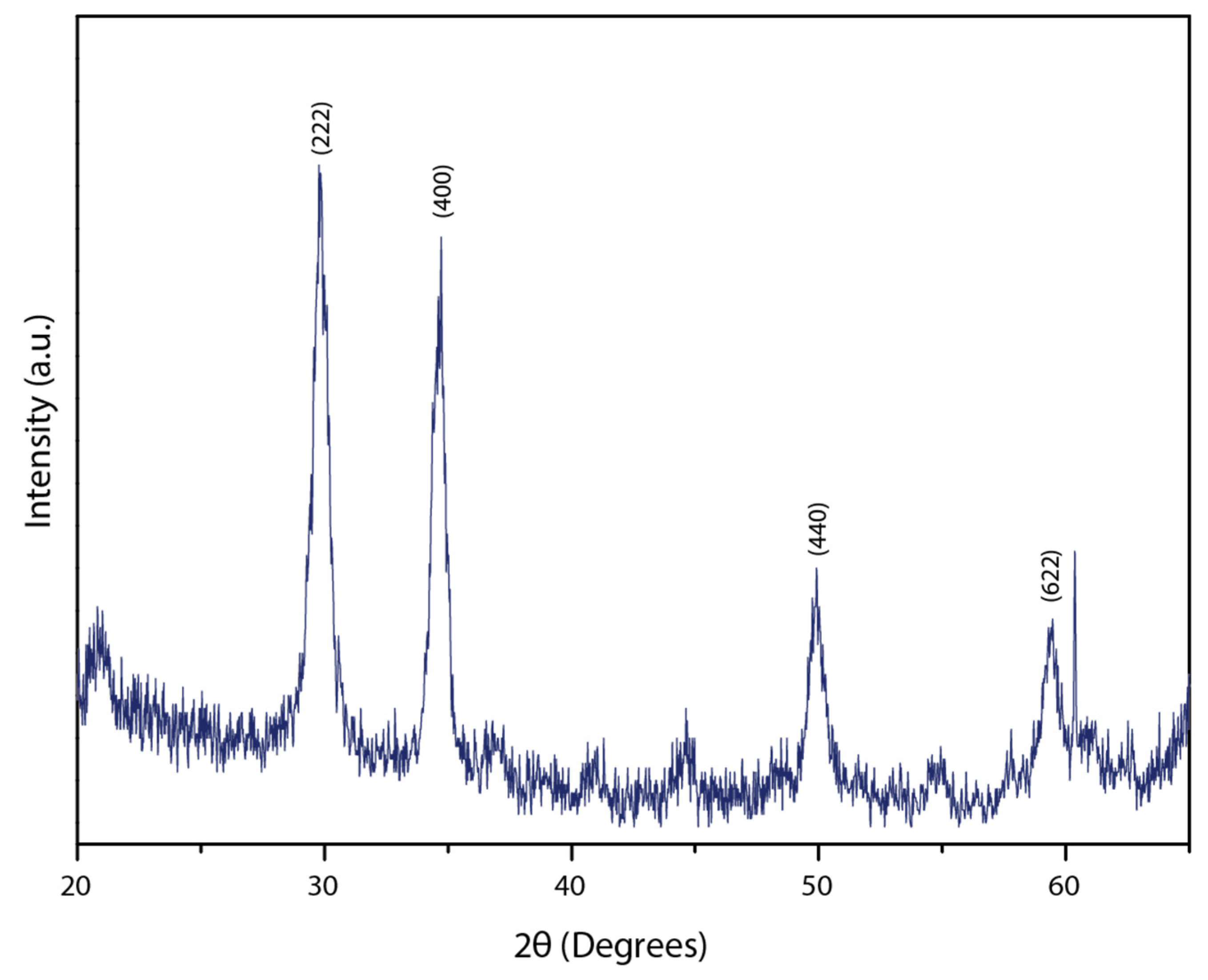
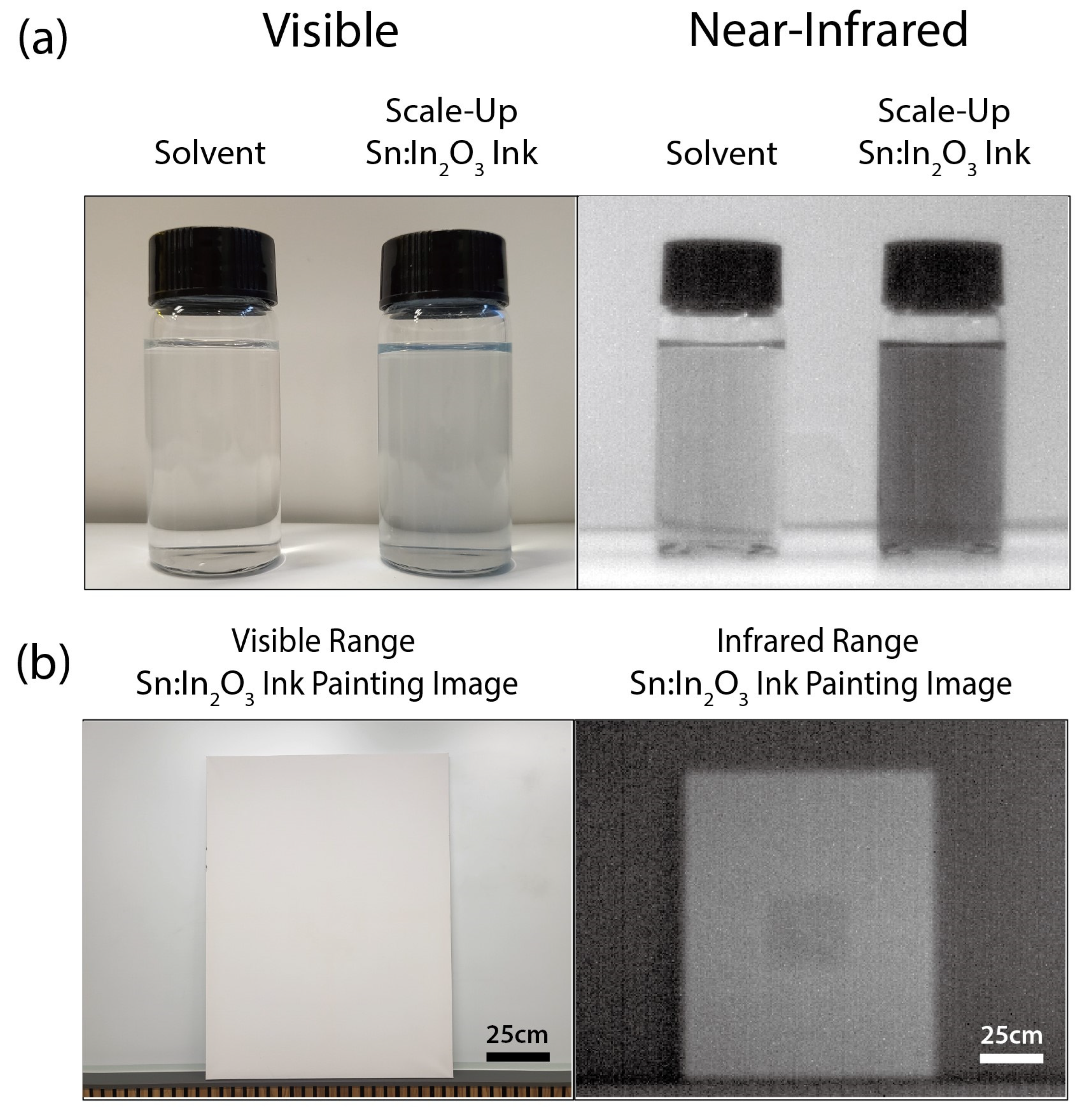
3. Results and Discussion

Scaled-up Sn:In2O3 NC infrared ink functionality is enabled through the introduction of an n-type tin dopant under colloidal synthetic conditions. Sn dopants are incorporated into the In2O3 lattice, substituting In atomic sites as degenerately doped Sn In . Free-electron carriers are generated within the NC lattice following the Kröger–Vink notation [2,21]. The intentional doping of n-type Sn dopant induces strong LSPR optical functionality in the near-infrared spectrum. Scaled-up Sn:In2O3 NCs similarly exhibited powerful LSPR optical functionality [22].
( 2 Sn In   ·   O i ) × 2 Sn In + 1 2 O 2   ( g ) + 2 e
Lab-scale Sn:In2O3 NCs were synthesized in a 50 mL 3-neck flask with the resulting solution adjusted to a concentration of 22 mg/mL with the addition of a hexane solvent (Figure 1a, left). The scaled-up Sn:In2O3 NCs were obtained and were then transferred to a 1 L total volume container. Hexane solvent was added to adjust the concentration to 30 mg/mL (Figure 1a, right). The synthesis process of Sn:In2O3 involves reaction with oleic acid with indium (III) acetate (In(Ac)3) to produce indium oleate (In(Oleate)3) and then form indium oxide. At this time, indium oxide was doped with tin to synthesize Sn:In2O3. Indium acetate and oleic acid were coordinated to form indium oleate precursor, and when injected into oleyl alcohol using the continuous injection method, it undergoes NC growth through the condensation reaction of indium oleate and oleyl alcohol [23]. At this time, all other conditions are the same, only the injection rate is changed to 0.2 mL/min for synthesis (Figure 1b, left). A continuous precursor injection batch reactor setup for the scaled-up synthetic reaction is shown (Figure 1b, right).
NCs were observed using SEM imaging, and in a scaled-up synthetic batch, well-defined NC particle appearance was observed (Figure 2a). The Sn:In2O3 NC solution spectrum was obtained and measured via FTIR, complemented with a Drude model analysis using MATLAB (2023b) fitting [24]. The experimentally collected scaled-up LSPR peak value (2537 cm−1) and MATLAB fitted value (2586 cm−1) well matches within the infrared absorption region of interest. The experimentally collected lab-scale LSPR peak value (1951 cm−1) and MATLAB fitted value (1962 cm−1) well matches within the infrared absorption region of interest. The LSPR extinction resonance frequency is dependent on the dopant activation of the Sn dopant precursor. As the n-type dopant activation concentration within the confines of the NC lattice increases, the free-carrier electron density increases and moves to higher frequencies. Due to a higher reactor volume in the scaled-up reactor, dopant activation may be varied due to degassing synthetic conditions and scalability, but the intrinsic LSPR absorption property is still realized. Therefore, scaled-up Sn:In2O3 NC inks at a dopant precursor concentration of 5% are observed in the higher frequency region due to higher population of free carriers within the NCs. And variations may be tamed through dopant activation control through precursor concentration fine-tuning. Because LSPR is an interfacial and dielectric phenomenon, the LSPR extinction response can be simulated and fitted through the Drude model (Figure 2b) [25]. Fourier-transform infrared spectroscopy (FTIR) was used to measure infrared absorption over a wider wavelength range. FTIR was employed to analytically characterize the infrared extinction LSPR response by extracting optoelectronic material property parameters [26].
ϵ p = ϵ ω p 2 ω 2 + i ω γ  
The Drude model was used to extract the concentration of degenerately doped free-electron carriers confined within Sn:In2O3 NCs [27,28]. ϵ p represents the optical extinction characteristics of plasmonic metal oxides in the equation above, and ω is a function of the wavenumber. The Drude model is operated by an external incident electromagnetic field beyond the infrared range. It is treated as a vibration of a free-electron gas [27]. The position of the extinction peak depends on the plasma frequency ω p   according to the concentration of free electrons n e . The absorption coefficient α is a function of the wavenumber ω. It is determined by the imaginary loss coefficient part of ϵ p = n k i . The relationship between the absorption and imaginary loss coefficients is α = 4πk/λ. The wavelength λ can be converted to the wavenumber 1/ω (cm−1) [14,27,28]
ω p = n e e 2 ε 0 m *
The bulk plasma frequency is determined by the influence of ω p . The free-electron concentration is n e , and the constant e is the fundamental electron charge. ε 0 is the permittivity of free space, and m* is the electron effective mass. The damping parameter γ is a function of frequency-dependent ω . An extended Drude model is thus employed, where γ L is the low-frequency damping constant, γ H the high-frequency damping constant, γ X the crossover frequency, and γ W the cross-over width.
γ ( ω ) = γ L γ L γ H π [ t a n 1 ( ω γ X γ W ) + π 2 ]
We estimated the relationship between the observed LSPR peak and the free carrier density confined within the NCs (Table 1) [29]. The free carrier density of Sn-doped scaled-up Sn:In2O3 NCs was estimated to be 2.53 × 1020 cm−3. And the free carrier density of Sn-doped lab-scale Sn:In2O3 NCs was estimated to be 1.44 × 1020 cm−3. The free carrier density of doped Sn:In2O3 NCs varies according to the degree of the doping of the Sn. Scaled-up Sn:In2O3 NCs were confirmed to be metallically degenerately doped and incorporated into the NC lattice adequately. Even with the scaled-up synthetic procedure, the material characteristics in infrared absorption through the LSPR effect is observed [30]. FTIR measurements were characterized in a mid-infrared transparent solvent. The selected dielectric medium in the FTIR liquid cell is suitable for dispersion and has a dielectric constant of 1.505, which is tetrachloroethylene (TCE) [31]. Spectral fitting using the Drude model via MATLAB was conducted under solution dispersion in this dielectric medium solution. The XRD pattern of scaled-up Sn:In2O3 NC infrared ink shows peaks corresponding to (222), (400), (440), and (662) bixbyite phase indium oxide, confirming nanoparticle crystallinity after synthesis (Figure 3) [31,32].
Scaled-up Sn:In2O3 NCs exhibited optical properties similar to those at lab scale in previous studies demonstrating a free carrier density range of 1020 cm−3 [33]. Free electrons plasmonically resonate with infrared waves, resulting in intense mid-infrared LSPR absorption. A dispersion solution of Sn:In2O3 NCs in hexane at a concentration of 10 mg/mL visually appears blue, attributed to the infrared absorption tail absorbing the red visible light spectrum (Figure 4a, left). The identical Sn:In2O3 NCs solution observation was made using a near-infrared InGaAs camera covering the range from 900 nm to 1700 nm, exhibiting strong opacity to infrared (Figure 4a, right) [34]. We further utilized Sn:In2O3 NC ink in a colorant surfactant application by painting a square shape on a 130 cm × 97 cm art canvas surface by brush. With the naked eye, in the visible spectrum, no apparent marking was observed on the canvas surface (Figure 4b, left). With the same canvas surface when photographed with an infrared camera, the painted square pattern surface area is optically discrete and discernable over a wide surface area (Figure 4b, right) [35].

4. Conclusions

The successful scale-up of Sn-doped Sn:In2O3 NC infrared ink functionality was achieved through the introduction of n-type tin dopants under controlled large-batch colloidal synthetic conditions. The Sn dopants are incorporated into the In2O3 lattice, substituting for In atomic sites as degenerately doped Sn In generating free-electron carriers within the NC lattice, procreating metallic degenerately doped NCs. This doping process induces strong LSPR optical functionality in the near-infrared spectrum, which is maintained in scaled-up batches of Sn NCs. Expanded Sn:In2O3 NCs showed infrared LSPR activity, observed in laboratory-scale synthesis study procedures. With a near-infrared InGaAs camera, we were able to see the state of dispersion in hexane and the absorption of infrared rays after painting on an art canvas.
The optical properties of scaled-up Sn:In2O3 NCs with an estimated free carrier density of 2.53 × 1020 cm−1 mirror those observed in a lab-scale synthetic sample. This consistency demonstrates that the scale-up process does not compromise the material optical performance as a metallic degenerately doped plasmonic nanocrystal. The NC ink as a dilute thin film is visibly transparent, while the concentrated NC solution dispersed in hexane exhibits a unique blue color due to visible red wavelength absorption. Strong opacity to the infrared electromagnetic spectrum was confirmed using the InGaAs camera. As a practical application, Sn-doped NC ink proves effective as a colorant surfactant, producing visible markings only under infrared imaging. SEM imaging confirms the well-defined NC particle distribution in hexane, and FTIR, complemented by Drude model analysis, verified the LSPR peak values and the infrared absorption characteristics. The synthetic process for scale-up involves a continuous precursor injection batch reactor, ensuring uniform doping and consistent NC quality. The scaled-up Sn-doped NCs exhibit crystallinity, as confirmed by XRD patterns, with peaks corresponding to the bixbyite phase of indium oxide. Scanning electron microscopy (SEM) and XRD were used to observe the formation of spherical Sn:In2O3 NCs with crystallinity.
Even as the scale of the experiment increases, the same LSPR phenomenon can be observed. This study suggests the feasibility of the mass production of Sn:In2O3 NCs. Mass production can bring significant industrial benefits due to the fact that the raw material cost is 10 times lower, and the synthesis capacity is 20 times larger, which can significantly reduce the economic cost of production. Mass-produced metal-modified doped Sn:In2O3 nanocrystalline ink can be applied to a wide range of materials across industries. It can be applied to smart windows, photocatalysts, light sensors, and all other fields that require infrared blocking and visible light transparency. It can also be used as an infrared marker for security purposes, contributing to the advancement of application technology of infrared semiconductor NCs.

Author Contributions

Conceptualization, S.-H.C.; methodology and investigation, D.-Y.P. and S.-H.C. All authors have read and agreed to the published version of the manuscript.

Funding

This work was supported by the Bisa Research Grant of Keimyung University in 2023 (20220648).

Data Availability Statement

The original contributions presented in the study are included in the article, further inquiries can be directed to the corresponding author.

Acknowledgments

We thank the Korea Basic Science Institute (KBSI) Daegu user facility for analytical HR-SEM equipment support.

Conflicts of Interest

The authors declare no conflicts of interest.

References

  1. Agrawal, A.; Cho, S.H.; Zandi, O.; Ghosh, S.; Johns, R.W.; Milliron, D.J. Localized Surface Plasmon Resonance in Semiconductor Nanocrystals. Chem. Rev. 2018, 118, 3121–3207. [Google Scholar] [CrossRef]
  2. Kanehara, M.; Koike, H.; Yoshinaga, T.; Teranishi, T. Indium Tin Oxide Nanoparticles with Compositionally Tunable Surface Plasmon Resonance Frequencies in the Near-IR Region. J. Am. Chem. Soc. 2009, 131, 17736–17737. [Google Scholar] [CrossRef] [PubMed]
  3. König, T.A.F.; Ledin, P.A.; Kerszulis, J.; Mahmoud, M.A.; El-Sayed, M.A.; Reynolds, J.R.; Tsukruk, V.V. Electrically Tunable Plasmonic Behavior of Nanocube–Polymer Nanomaterials Induced by a Redox-Active Electrochromic Polymer. ACS Nano 2014, 8, 6182–6192. [Google Scholar] [CrossRef]
  4. Cortés, E.; Besteiro, L.V.; Alabastri, A.; Baldi, A.; Tagliabue, G.; Demetriadou, A.; Narang, P. Challenges in Plasmonic Catalysis. ACS Nano 2020, 14, 16202–16219. [Google Scholar] [CrossRef]
  5. Hansen, H.E.; Berge, T.B.; Seland, F.; Sunde, S.; Burheim, O.S.; Pollet, B.G. Towards Scaling up the Sonochemical Synthesis of Pt-Nanocatalysts. Ultrason. Sonochem. 2024, 103, 106794. [Google Scholar] [CrossRef] [PubMed]
  6. Kim, J.-H.; Chon, M.-W.; Choa, S.-H. Technology of Flexible Transparent Conductive Electrode for Flexible Electronic Devices. J. Microelectron. Packag. Soc. 2014, 21, 1–11. [Google Scholar] [CrossRef]
  7. Llordés, A.; Garcia, G.; Gazquez, J.; Milliron, D.J. Tunable Near-Infrared and Visible-Light Transmittance in Nanocrystal-in-Glass Composites. Nature 2013, 500, 323–326. [Google Scholar] [CrossRef]
  8. Wang, K.; Meng, Q.; Wang, Q.; Zhang, W.; Guo, J.; Cao, S.; Elezzabi, A.Y.; Yu, W.W.; Liu, L.; Li, H. Advances in Energy-Efficient Plasmonic Electrochromic Smart Windows Based on Metal Oxide Nanocrystals. Adv. Energy Sustain. Res. 2021, 2, 2100117. [Google Scholar] [CrossRef]
  9. Leppäniemi, J.; Eiroma, K.; Majumdar, H.; Alastalo, A. Far-UV Annealed Inkjet-Printed In2O3 Semiconductor Layers for Thin-Film Transistors on a Flexible Polyethylene Naphthalate Substrate. ACS Appl. Mater. Interfaces 2017, 9, 8774–8782. [Google Scholar] [CrossRef] [PubMed]
  10. Cummins, G.; Desmulliez, M.P.Y. Inkjet Printing of Conductive Materials: A Review. Circuit World 2012, 38, 193–213. [Google Scholar] [CrossRef]
  11. Sasaki, T.; Endo, Y.; Nakaya, M.; Kanie, K.; Nagatomi, A.; Tanoue, K.; Nakamura, R.; Muramatsu, A. One-Step Solvothermal Synthesis of Cubic-Shaped ITO Nanoparticles Precisely Controlled in Size and Shape and Their Electrical Resistivity. J. Mater. Chem. 2010, 20, 8153–8157. [Google Scholar] [CrossRef]
  12. Hong, S.-J.; Kim, Y.-H.; Han, J.-I. Development of Ultrafine Indium Tin Oxide (ITO) Nanoparticle for Ink Jet Printing by Low Temperature Synthetic Method. In Proceedings of the 2006 IEEE Nanotechnology Materials and Devices Conference, Gyeongju, Republic of Korea, 22–25 October 2006; Volume 1, pp. 464–465. [Google Scholar] [CrossRef]
  13. Hong, S.-J.; Kim, J.-W.; Lim, J.-W.; Choi, G.-S.; Isshiki, M. Characteristics of Printed Thin Films Using Indium Tin Oxide (ITO) Ink. Mater. Trans. 2010, 51, 1905–1908. [Google Scholar] [CrossRef]
  14. Runnerstrom, E.L.; Bergerud, A.; Agrawal, A.; Johns, R.W.; Dahlman, C.J.; Singh, A.; Selbach, S.M.; Milliron, D.J. Defect Engineering in Plasmonic Metal Oxide Nanocrystals. Nano Lett. 2016, 16, 3390–3398. [Google Scholar] [CrossRef]
  15. Yin, P.; Hegde, M.; Tan, Y.; Chen, S.; Garnet, N.; Radovanovic, P.V. Controlling the Mechanism of Excitonic Splitting in In2O3 Nanocrystals by Carrier Delocalization. ACS Nano 2018, 12, 11211–11218. [Google Scholar] [CrossRef] [PubMed]
  16. Saez Cabezas, C.A.; Sherman, Z.M.; Howard, M.P.; Dominguez, M.N.; Cho, S.H.; Ong, G.K.; Green, A.M.; Truskett, T.M.; Milliron, D.J. Universal Gelation of Metal Oxide Nanocrystals via Depletion Attractions. Nano Lett. 2020, 20, 4007–4013. [Google Scholar] [CrossRef]
  17. Benny, S.; Vidyanagar, A.V.; Bhat, S.V. Progress and Prospects with Cationic and Anionic Doping of Solution-Processed Kesterite Solar Absorbers: A Mini-Review. Energy Fuels 2024, 38, 61–72. [Google Scholar] [CrossRef]
  18. Kim, C.; Park, J.-W.; Kim, J.; Hong, S.-J.; Lee, M.J. A Highly Efficient Indium Tin Oxide Nanoparticles (ITO-NPs) Transparent Heater Based on Solution-Process Optimized with Oxygen Vacancy Control. J. Alloys Compd. 2017, 726, 712–719. [Google Scholar] [CrossRef]
  19. Maho, A.; Saez Cabezas, C.A.; Meyertons, K.A.; Reimnitz, L.C.; Sahu, S.; Helms, B.A.; Milliron, D.J. Aqueous Processing and Spray Deposition of Polymer-Wrapped Tin-Doped Indium Oxide Nanocrystals as Electrochromic Thin Films. Chem. Mater. 2020, 32, 8401–8411. [Google Scholar] [CrossRef]
  20. Jansons, A.W.; Hutchison, J.E. Continuous Growth of Metal Oxide Nanocrystals: Enhanced Control of Nanocrystal Size and Radial Dopant Distribution. ACS Nano 2016, 10, 6942–6951. [Google Scholar] [CrossRef]
  21. Cho, S.H.; Roccapriore, K.M.; Dass, C.K.; Ghosh, S.; Choi, J.; Noh, J.; Reimnitz, L.C.; Heo, S.; Kim, K.; Xie, K.; et al. Spectrally Tunable Infrared Plasmonic F,Sn:In2O3 Nanocrystal Cubes. J. Chem. Phys. 2020, 152, 014709. [Google Scholar] [CrossRef]
  22. Wang, J.; Zeng, P.; Xiao, X.; Zhou, C.; Wei, H.; Yu, C. Recent Advances in Nanostructured Substrates for Surface-Enhanced Infrared Absorption Spectroscopy. Nanotechnology 2023, 34, 382002. [Google Scholar] [CrossRef]
  23. Xiao, F.; Xu, W.; Liu, H.; Li, H.; Yu, H.; Hao, B. Optically Compatible Infrared Camouflage Performance of ITO Ink. RSC Adv. 2024, 14, 17355–17363. [Google Scholar] [CrossRef]
  24. Gibbs, S.L.; Dean, C.; Saad, J.; Tandon, B.; Staller, C.M.; Agrawal, A.; Milliron, D.J. Dual-Mode Infrared Absorption by Segregating Dopants within Plasmonic Semiconductor Nanocrystals. Nano Lett. 2020, 20, 7498–7505. [Google Scholar] [CrossRef]
  25. Conti III, C.R.; Quiroz-Delfi, G.; Schwarck, J.S.; Chen, B.; Strouse, G.F. Carrier Density, Effective Mass, and Nuclear Relaxation Pathways in Plasmonic Sn:In2O3 Nanocrystals. J. Phys. Chem. C 2020, 124, 28220–28229. [Google Scholar] [CrossRef]
  26. Mendelsberg, R.J.; Garcia, G.; Li, H.; Manna, L.; Milliron, D.J. Understanding the Plasmon Resonance in Ensembles of Degenerately Doped Semiconductor Nanocrystals. J. Phys. Chem. C 2012, 116, 12226–12231. [Google Scholar] [CrossRef]
  27. Mendelsberg, R.J.; Garcia, G.; Milliron, D.J. Extracting Reliable Electronic Properties from Transmission Spectra of Indium Tin Oxide Thin Films and Nanocrystal Films by Careful Application of the Drude Theory. J. Appl. Phys. 2012, 111, 063515. [Google Scholar] [CrossRef]
  28. Mergel, D.; Qiao, Z. Dielectric Modelling of Optical Spectra of Thin In2O3 : Sn Films. J. Phys. D Appl. Phys. 2002, 35, 794. [Google Scholar] [CrossRef]
  29. Araujo, J.J.; Brozek, C.K.; Liu, H.; Merkulova, A.; Li, X.; Gamelin, D.R. Tunable Band-Edge Potentials and Charge Storage in Colloidal Tin-Doped Indium Oxide (ITO) Nanocrystals. ACS Nano 2021, 15, 14116–14124. [Google Scholar] [CrossRef]
  30. Buonsanti, R.; Llordes, A.; Aloni, S.; Helms, B.A.; Milliron, D.J. Tunable Infrared Absorption and Visible Transparency of Colloidal Aluminum-Doped Zinc Oxide Nanocrystals. Nano Lett. 2011, 11, 4706–4710. [Google Scholar] [CrossRef]
  31. Cho, S.H.; Ghosh, S.; Berkson, Z.J.; Hachtel, J.A.; Shi, J.; Zhao, X.; Reimnitz, L.C.; Dahlman, C.J.; Ho, Y.; Yang, A.; et al. Syntheses of Colloidal F:In2O3 Cubes: Fluorine-Induced Faceting and Infrared Plasmonic Response. Chem. Mater. 2019, 31, 2661–2676. [Google Scholar] [CrossRef]
  32. Suzuki, R.; Nishi, Y.; Matsubara, M.; Muramatsu, A.; Kanie, K. Single-Crystalline Protrusion-Rich Indium Tin Oxide Nanoparticles with Colloidal Stability in Water for Use in Sustainable Coatings. ACS Appl. Nano Mater. 2020, 3, 4870–4879. [Google Scholar] [CrossRef]
  33. Sun, X.W.; Huang, H.C.; Kwok, H.S. On the Initial Growth of Indium Tin Oxide on Glass. Appl. Phys. Lett. 1996, 68, 2663–2665. [Google Scholar] [CrossRef]
  34. Kalinin, S.V.; Roccapriore, K.M.; Cho, S.H.; Milliron, D.J.; Vasudevan, R.; Ziatdinov, M.; Hachtel, J.A. Separating Physically Distinct Mechanisms in Complex Infrared Plasmonic Nanostructures via Machine Learning Enhanced Electron Energy Loss Spectroscopy. Adv. Opt. Mater. 2021, 9, 2001808. [Google Scholar] [CrossRef]
  35. Lozovoy, K.A.; Korotaev, A.G.; Kokhanenko, A.P.; Dirko, V.V.; Voitsekhovskii, A.V. Kinetics of Epitaxial Formation of Nanostructures by Frank–van Der Merwe, Volmer–Weber and Stranski–Krastanow Growth Modes. Surf. Coat. Technol. 2020, 384, 125289. [Google Scholar] [CrossRef]
Figure 1. (a) Lab-scale Sn:In2O3 NC batch of 10 mL product result (left) and scaled-up Sn:In2O3 NC batch of 1000 mL product result (right). (b) Lab-scale batch reactor synthesis mechanism and experimental schematic (left) and 1000 mL continuous injection scale-up batch reactor setup (right).
Metals 14 00843 g001
Figure 2. (a) SEM image of observed Sn:In2O3 NCs shows that NC product is dispersed in hexane solution at 30 mg/mL concentration. (b) FTIR spectrum of scaled-up and lab-scale Sn:In2O3 NCs and MATLAB Drude model fitting.
Metals 14 00843 g002
Figure 3. XRD pattern of scaled-up Sn:In2O3 NC infrared ink with dominantly observed (222), (400), (440), and (622) diffraction peaks.
Metals 14 00843 g003
Figure 4. (a) Comparison photo in the visible spectrum of vial containing solvent (hexane) and scaled-up Sn:In2O3 NC dispersed ink at 30 mg/mL diluted concentration. (b) Additionally, a cubic painting drawn on an art canvas solid surface using Sn:In2O3 ink is shown. The left side shows the visible spectral range photo, while the right side displays the infrared image taken using a near-infrared InGaAs camera at a 900 nm to 1700 nm detection range.
Metals 14 00843 g004
Table 1. Drude model LSPR properties.
PropertiesScale Up
Parameter
Lab Scale
Parameter
LSPR Peak
[cm−1]
25371962
Free Carrier Density
n e [cm−3]
2.53 × 10201.44 × 1020
Bulk Plasma Frequency
ω p [cm−1]
75255670
Low-Frequency Damping Constant
γ L [cm−1]
15691582
High-Frequency Damping Constant
γ H [cm−1]
36086
Crossover Frequency
γ X [cm−1]
44473507
Crossover Width
γ W [cm−1]
277311
Disclaimer/Publisher’s Note: The statements, opinions and data contained in all publications are solely those of the individual author(s) and contributor(s) and not of MDPI and/or the editor(s). MDPI and/or the editor(s) disclaim responsibility for any injury to people or property resulting from any ideas, methods, instructions or products referred to in the content.

